國 立 交 通 大 學
電子工程學系 電子研究所碩士班
碩 士 論 文
SONOS快閃記憶體中寫入電荷和元件結構
對於隨機電報雜訊的影響
Program Charge Effect on Random Telegraph Noise
Amplitude and Its Device Structural Dependence in
SONOS Flash Memory
研 究 生 :林東陽
指導教授 :汪大暉 博士
SONOS快閃記憶體中寫入電荷和元件結構
對於隨機電報雜訊的影響
Program Charge Effect on Random Telegraph
Noise Amplitude and Its Device Structural
Dependence in SONOS Flash Memory
研 究 生 : 林東陽 Student : Steven Lin
指導教授 : 汪大暉 博士 Advisor : Dr. Tahui Wang
國立交通大學
電子工程學系 電子研究所碩士班
碩士論文
A Thesis
Submitted to Department of Electronics Engineering & Institute
of Electronics College of Electrical and Computer Engineering
National Chiao Tung University
in Partial Fulfillment of the Requirements
for the Degree of Master of Science
in Electronics Engineering
July 2010
Hsinchu, Taiwan, Republic of China.
i
SONOS快閃記憶體中寫入電荷和元件結構
對於隨機電報雜訊的影響
學生:林東陽 指導教授:汪大暉 博士
國立交通大學電子工程學系電子研究所碩士班
摘要
在本篇論文中,我們研究了氮化矽快閃式記憶體(SONOS Flash Memory)中的 寫入載子對隨機電報雜訊(Random Telegraph Noise)之振幅的影響。同時,我們對 浮動閘極快閃式記憶體(Floating Gate Flash Memory)、平面式氮化矽記憶體及鰭 狀(FinFET)氮化矽快閃式記憶體做了測量與模擬的工作。我們發現平面式氮化矽 記憶元件在資料寫入後隨機電報雜訊振幅分布得寬廣,而浮動閘極記憶元件在資 料寫入前後有相同的隨機電報雜訊振幅。在平面式氮化矽記憶體的情況下之所以 分布得寬廣歸因於隨機且分離的寫入載子造成的電流路徑滲透作用。因此在建立 氮化矽快閃式記憶體中隨機電報雜訊的模型時,必須將寫入載子效應納入考慮。 在氮化矽記憶體中隨機電報雜訊的寫入載子效應可由類似包覆式閘極的結 構顯著減少,例如鰭狀的結構,利用較高的寫入載子分布對稱性來降低寫入載子 效應。
ii
Program Charge Effect on Random Telegraph
Noise Amplitude and Its Device Structural
Dependence in SONOS Flash Memory
Student:Steven Lin Advisor:Dr. Tahui Wang
Department of Electronics Engineering & Institute of Electronics
National Chiao Tung University
ABSTRACT
Nitride program charge effect on the amplitude of random telegraph noise (RTN) in SONOS flash cells is investigated. We measure and simulate RTN amplitudes in floating gate flash, planar SONOS, and FinFET SONOS cells. We find that a planar SONOS has a wide spread in RTN amplitudes after programming while a floating gate flash cell has identical RTN amplitudes in erase and program states. The spread of program-state RTN in a planar SONOS is attributed to a current-path percolation effect caused by random discrete nitride charges. Consequently, program charge effect has to be taken into consideration while establishing RTN model in SONOS.
The RTN amplitude spread can be significantly reduced in a surrounding gate structure, such as FinFET SONOS, due to a higher degree of symmetry in a program charge distribution.
iii
誌
謝
儘管兩年的研究所生活過得相當快,但過程仍精彩且充實。首先,這本碩士 論文的完成,必須感謝我的指導教授:汪大暉教授,老師紮實的研究訓練,讓我 在學業上與研究上碰到的困難,都能秉持正確的態度來面對。除此之外,老師做 研究的方法和嚴謹、積極的處事之道也是我學習的榜樣,在此深表我對老師的感 謝。 在此我要感謝學長姐們,包括小馬、達叔、佑亮、標叔、志昌、智雄、文仙, 帶我走過研究所的兩年生活,給予我人生上、學業上各種重要的建議和引導。在 此要特別感謝小馬學長,實驗與理論上遇到困難時,總是不吝解惑,無私地教導 讓我從中成長許多。以及達叔,時常給予我關懷,也傳承給我許多人生經驗。還 要感謝標叔與佑亮平時給予我的指導,在論文寫作期間不斷給我建言和鼓勵,讓 畢業和論文能夠如期完成。感謝在兩年碩士生涯與我一起成長的莊老師研究群同 學:元宏、永涵、士嵩、政穎在生活上和研究上的幫忙,讓我的實驗室生活充滿 樂趣。以及各位學弟:岳庭、明偉、志宇、書祥,感謝你們對實驗室的付出,也 讓我們一起快樂的相處一年多。 最後,感謝我的父母、家人和女友,在求學期間給予我鼓勵和支持,讓我能 順利地、毫無顧忌地完成碩士學位。iv
Contents
Chinese Abstract --- i English Abstract --- ii Acknowledgements --- iii Contents --- iv Figure Captions --- viChapter 1 Introduction
1
Chapter 2
Trap Position Extraction and Relation between RTN Amplitude
and Percolation Effect
5
2.1 Introduction……….……….. 52.2 Measurement of RTN……….…... 6
2.3 Extraction of Trap Position…………... 6
2.4 Current Percolation Effect and RTN Amplitude………...… 7
2.5 Percolation Effect Induced RTN Vt Distribution………..…… 7
Chapter 3 Program Charge Effect on Random Telegraph Noise Amplitude in
Floating Gate and SONOS Flash Memory
18
3.1 Introduction……….…... 183.2 Measurement of RTN Amplitude in MLC Flash………... 18
3.3 Statistics Result of Program-state and Erase-state RTN……….………...…. 19
3.4 Correlation Factor for Program-state and Erase-state RTN……….. 20
3.5 P/E Cycle Dependence of RTN……… 20
3.6 3D Atomistic Simulation of RTN………..….. 21
Chapter 4 Device Structural Dependence on Random Telegraph Noise in
SONOS Flash Memory
v
4.1 Introduction………...………… 36
4.2 Program Charge Effect on RTN in FinFET SONOS……….…………..…..…... 35
4.3 Degree of Inversion in FinFET SONOS………..……. 36
4.4 Channel Width Effect on Program Charge Induced Percolation Effect... 36
4.5 Symmetry of Program Charge Distribution in a Surrounding Gate SONOS…………... 37
Chapter 5 Conclusion
47
References
………..………...….48
vi
Figure Captions
Chapter 1
Fig. 1.1 Estimation of threshold voltage shift as a function of process node
Fig. 1.2 (a)Noise distributions of 90nm, 70nm, 50nm flash memory technologies
and (b)Measured Vth distribution of a 4-level MLC with level2 enlarged.
Chapter 2
Fig. 2.1 (a)The origin of RTN, (b) RTN phenomenon with the band diagram in
interface
Fig. 2.2 Typical drain current RTN of time domain plot pointing out the three major
parameters of RTS noise.
Fig. 2.3 The experimental setup for measuring random telegraph noise Fig. 2.4 Illustration of the objects meaning in trap position extraction
Fig. 2.5 Cumulative trap position distribution along the channel. Lg is the channel
length and Lt is the distance of the trap to the source
Fig. 2.6 An illustration of random dopant induced percolation effect.
Fig. 2.7 Illustration of Different RTN amplitude caused by two different percolation
path
Fig. 2.8 Cumulative probability of RTN induced Vt shift for different NOR
technologies ranging from 180nm to 45nm.
Fig. 2.9 The measurement and simulation data of cumulative probabilities versus
RTN induced Vt shift in 45nm SONOS cells.
Chapter 3
Fig. 3.1 Schematic illustration of source-side injection for split-gate structure
vii
Fig. 3.2 RTN amplitude versus drain current in a FG flash cell at two program
window : 1V, 2V. The drain voltage in measurement is 0.7V and the gate voltage is varied.
Fig. 3.3 RTN amplitude versus drain current in a SONOS flash cell at two program
window : 0.8V, 1.5V. The drain voltage in measurement is 0.7V and the gate voltage is varied.
Fig. 3.4 Measured program-state RTN amplitude versus erase-state RTN amplitude
in 40 FG flash cells. The RTN amplitude is measured at Id=500nA
@Vd=0.7V. The device dimension is W/L=0.11 m/0.09 m. The program
window is 1V or 2V.
Fig. 3.5 Measured program-state RTN amplitude versus erase-state RTN amplitude
in 60 planar SONOS cells. The RTN amplitude is measured at Id=500nA
@Vd=0.7V. The SONOS cells have W/L=0.09 m /0.08 m, a 2.8nm
tunnel oxide, a 6nm SiN and a 6nm top oxide.
Fig. 3.6 RTN amplitude versus drain current in a FG flash cell in three P/E cycles.
The Vt window is 1V. The drain voltage in measurement is 0.7V and the
gate voltage is varied.
Fig. 3.7 RTN amplitude versus drain current in a SONOS cell in three P/E cycles.
The Vt window is 1V. The drain voltage in measurement is 0.7V and the
gate voltage is varied.
Fig. 3.8 Measured RTN waveform and Id versus Vg plot (a) in erase-state and (b) in
program-state of a SONOS cell. Electron trapping at an interface trap is manifested by a current discontinuity in the Id-Vg plot
Fig. 3.9 he waveform of two-level RTN current switching is observed in erase-state
and 1st and 2nd program-state.
Fig. 3.10 Simulation flow chart of our 3D atomistic simulation for RTN amplitude at
viii
Fig. 3.11 Simulated RTN amplitude versus drain current in a FG flash cell.
Program-state and erase-state have the same placement of substrate random dopants. The RTN trap is placed in the middle of the device.
Fig. 3.12 Simulated RTN amplitude versus drain current in a planar SONOS cell.
Program-state and erase-state have a fixed placement of substrate dopants. Ten different sets of random program charges are simulated. An RTN amplitude due to number fluctuation is calculated with continuous substrate doping and program charges.
Chapter 4
Fig. 4.1 Cross-section of a FinFET SONOS and the electron concentration contour in
the FinFET SONOS obtained from a 2D simulation.
Fig. 4.2 RTN amplitude versus drain current in a FinFET SONOS cell for two P/E
cycles.
Fig. 4.3 Program-state RTN amplitude versus erase-state RTN amplitude in 50
FinFET SONOS cells. The RTN is measured at Id=500nA @Vd=0.7V. The fin height is 40nm and the fin width is 25nm. The channel length is 80nm . The program window is 1V.
Fig. 4.4 Program-state RTN amplitude versus erase-state RTN amplitude in FinFET
SONOS cells. The fin width is 10nm. (a) RTN is measured at Id=500nA and (b) RTN is measured at Id=200nA.
Fig. 4.5 In a planar SONOS, percolation paths are widely distributed in the gate
width direction. In a FinFET SONOS, conducting paths are confined to a small region in the corner of the Si fin.
Fig. 4.6 Measurement of the correlation factor in FinFET SONOS with two different
fin width, 10 nanometer and 25 nanometer. The correlation factor increases from 0.82 to 0.94 as the fin width reduces from 25 nanometer to 10
ix
nanometer.
Fig. 4.7 A 3D RTN simulation in planar SONOS with different channel width. The
correlation factor is calculated based on a sample size of 40 devices.
Fig. 4.8 An illustration of three different structures in SONOS flash: planar, FinFET
and surrounding gate.
Table. 1 Measured RTN correlation factors in FG flash, planar SONOS and FinFET
- 1 -
Chapter 1
Introduction
Flash memory is a non-volatile computer data storage technology that can be electrically programmed, erased and read for so many times and won’t be lost after cutting off the power. It is primarily used in memory cards, USB flash drives, and solid-state drives for general storage and transfer of data between computers and other digital products. Nevertheless, with the advanced VLSI processing, the effect of a single electron on a typical device can be quite significant. Such effects will eventually cause fundamental scaling and reliability problems.
Random Telegraph Noise (RTN) phenomenon arising from electron emission and capture at an interface trap site [1-3] has been recognized as a new scaling concern in flash memory[4-8]. Vt fluctuations originated from a large-amplitude RTN
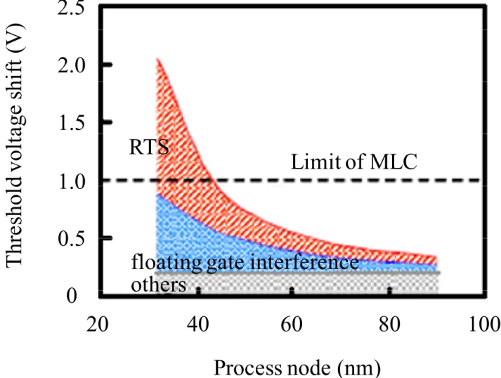
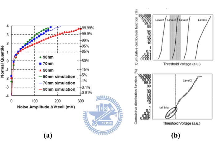
tail will cause a read error and become a prominent issue in designing a multilevel-cell (MLC) flash memory in 45nm technology node and beyond as shown in Fig. 1.1[6]. Fig. 1.2(a) shows that the worst case of RTN induced Vt shift is over 0.3V in 50 nanometer technology node [7]. Fig. 1.2(b) tells us that such large RTN tail may cause a read error in multilevel-cell flash memory application and requires the use of error code correction.
This thesis is composed of five chapters. After a review of RTN induced threshold voltage shift and read failure in flash memory in Chapter 1, we will introduce a technique of trap position extraction [9] and the concept of percolation effect in Chapter 2. In chapter 3, we will show you how program charges affect the
- 2 -
current path percolation in both floating gate and planar SONOS flash. In Chapter 4, we will discuss device structure dependence of RTN in SONOS flash. we will compare RTN measurement and simulation results in planar SONOS and FinFET SONOS. Finally in chapter 5, the conclusions will be presented.
- 3 -
Fig. 1.1 Estimation of threshold voltage shift as a function of process node
T
hre
shol
d vol
ta
ge
s
hi
ft
(V
)
Process node (nm)
2.5
2.0
1.5
1.0
0.5
0
20
40
60
80
100
RTS
floating gate interference
others
- 4 -
(a) (b)
Fig. 1.2 (a)Noise distributions of 90nm, 70nm, 50nm flash memory technologies
- 5 -
Chapter 2
Trap Position Extraction and Relation between
RTN Amplitude and Percolation Effect
2.1 Introduction
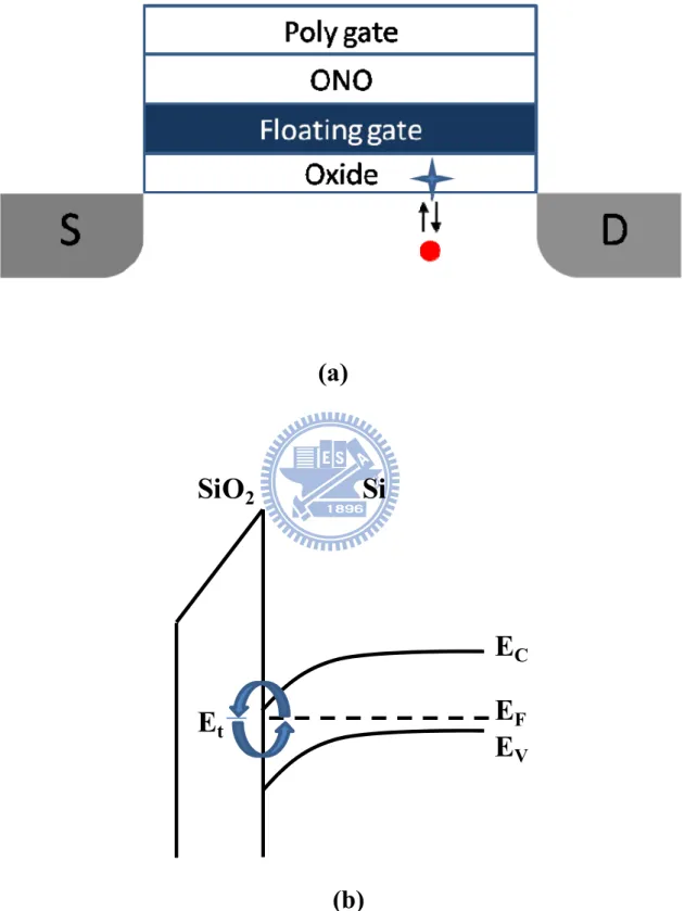
The origin of RTN is that single charge effect become more and more severe as device scaling down. As shown in Fig. 2.1(a), Trapping/detrapping of a single carrier charge in defect states near the Si/gate dielectric interface may lead current (or threshold voltage) to fluctuate and RTN amplitude will be even bigger in the coming technology node [6]. It will become a serious issue, not only in analog circuits, but also in dynamic random access memory, static random access memory and other digital application.
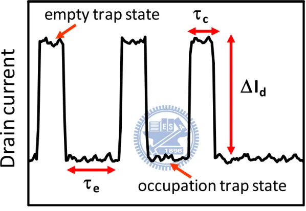
Fig. 2.2 is a typical time domain trace of RTN in drain current illustrating the three main RTS parameters: <τc>, <τe> and ΔId representing the average of the high
and low time constants and the magnitude of the current fluctuation. There is a formula concerning the relation between <τc> and <τe>:
RTN which makes current fluctuation occurs only when trap energy level (Et) close
enough to Fermi level. Traps with energy levels several kT below the Fermi level would be permanently filled where k and T are the Boltzmann’s constant and
exp(
)
c t F eE
E
g
kT
τ
τ
<
>
−
=
<
>
- 6 -
equilibrium temperature, respectively (Fig. 2.1(b)). While traps with energy levels several kT above the Fermi level would be permanently empty. Both of the two cases have no contribution to RTN.
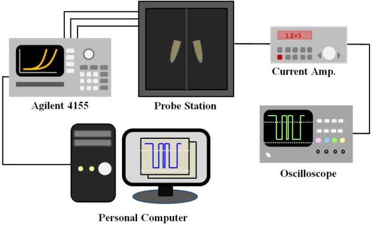
2-2 Measurement of RTN
The measurement setup is shown in Fig. 2.3. Agilent 4155C was used for our measurements on RTN. The sampling mode was selected, and the gate and drain bias were well controlled so that the trap energy level may close enough to Fermi level. With an appropriate sampling rate, the current fluctuation would be extracted and shown on the screen of 4155C.
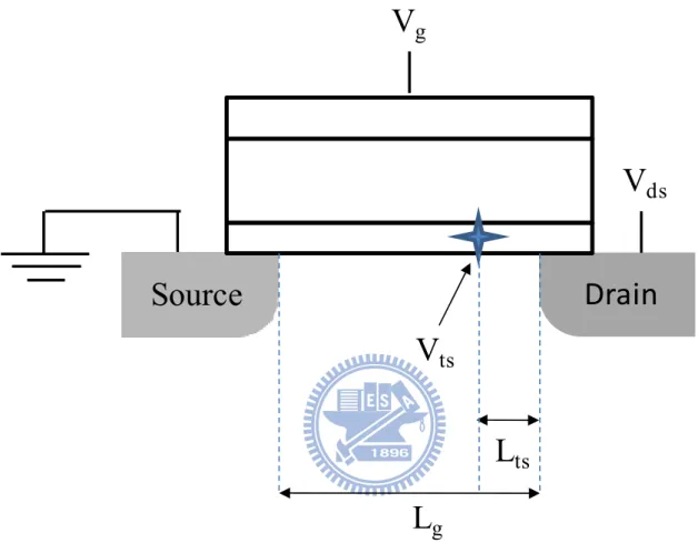
2-3 Extraction of the Trap Position
A convenient method based on 1D model proposed by IBM[9] can extract the lateral trap position in a cell. With linear region operation, the applied drain voltage (Vds) affects the trap linearly depending on its position in the device. Therefore, we
can apply different gate/drain bias to change the local potential at the trap site and sense the variation of <τc> and <τe>. As a result, the extraction of trap position along
the channel can be attained with the equation:
where Vts denotes the voltage raised at the trap position by the drain voltage and Lg is
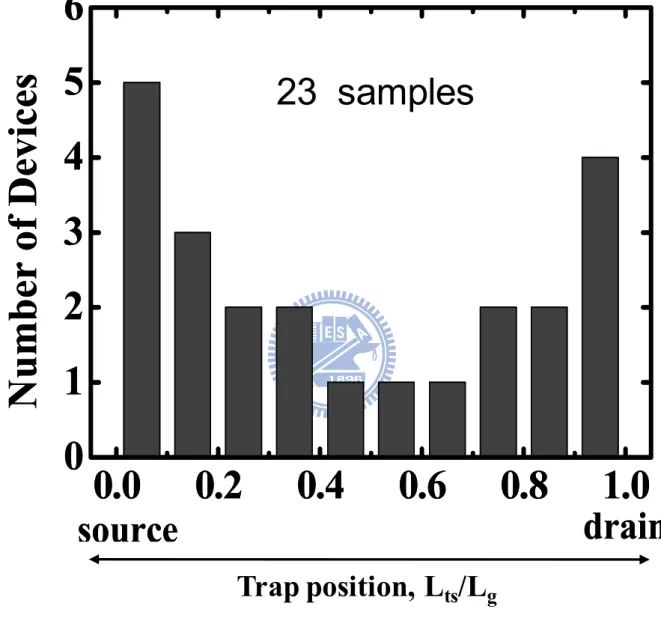
the channel length and Lts is the distance of the trap to the source (Fig. 2.4). Fig. 2.5 is
the profile of trap position along the channel. According the the experiment result, oxide trap are more likely to be located near the source/drain edge.
ts ts ds g
V
L
=
V
L
Δ
Δ
- 7 -
2-4 Current Percolation Effect and RTN Amplitude
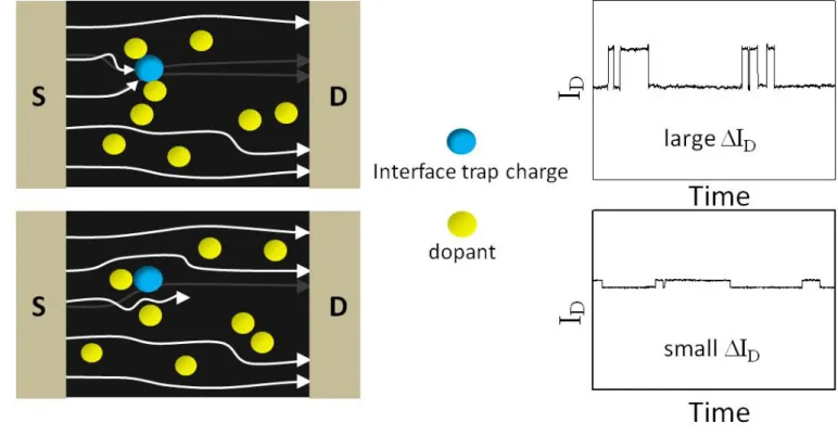
In an advanced device, number of substrate dopants is so small that cannot be regarded as an uniform doping concentration but a random and discrete distribution. Such discrete dopants may produce discrete potential barriers in channel surface (Fig. 2.6 [10]. Conducting carriers find a smoothest path to avoid these potential barriers as flowing from source to drain. This phenomenon is called current path percolation effect and more precisely in this case - random dopants induced percolation effect.
Random discrete dopant effects may vary RTN’s amplitude [11]. The illustration in Fig.2.7 exhibits two different random dopant distribution with two different current percolation pattern correspondingly. One the interface state trap an electron, the current flow will be affected at the same time. If the interface trapped-charge is located at the key spot for current percolation path, the RTN amplitude is relatively large (large ΔID). On the other hand, smaller RTN amplitude implies that
trapped-charge might be located at a minor spot for current percolation path, as shown in the lower case in Fig. 2.7.
2-5 Percolation Effect Induced RTN V
tDistribution
Recently, it has been reported that single-trap RTN amplitudes and thus Vt
fluctuations exhibit an exponential distribution experimentally and a statistical model based on a three-dimensional Monte Carlo simulation with the same consequence can be described as [12-14]: (Fig. 2.8)
- 8 - 1 ( ) exp( t) t V f V σ σ Δ Δ = −
In a FG flash memory for instance, the RTN tail is attributed to random dopant induced current-path percolation effects and σ is dependent on a substrate doping concentration, cell size and oxide thickness. The RTN amplitude distribution has a larger tail at a shorter gate length.
We also perform an experiment and 3D atomistic simulation on 45nm node planar SONOS flash cells to evaluate the distribution of Vt. Fig. 2.9 is the result with
200 simulations which also reveals the identical result that RTN induced Vt
fluctuation follows an exponential distribution. We will give you a brief simulation flow in the following Chapter 3.
- 9 -
(a)
(b)
Fig. 2.1 (a)The origin of RTN, (b) RTN phenomenon with the band diagram in
interface
SiO
2Si
E
tE
CE
VE
F- 10 -
Fig. 2.2 Typical drain current RTN of time domain plot pointing out the three major
parameters of RTS noise.
Time
Dr
a
in
c
u
rre
n
t
τ
c
τ
e
ΔI
d
empty trap state
occupation trap state
- 11 -
- 12 -
Fig. 2.4 Illustration of the objects meaning in trap position extraction
Source
Drain
L
tsL
gV
tsV
dsV
g- 13 -
Fig. 2.5 Cumulative trap position distribution along the channel. Lg is the channel
length and Lts is the distance of the trap to the source
0.0
0.2
0.4
0.6
0.8
1.0
0
1
2
3
4
5
6
Number of Devi
ces
source
drain
Trap Position,
x
t
L
(1- )
0.0
0.2
0.4
0.6
0.8
1.0
0
1
2
3
4
5
6
Number of Devi
ces
source
drain
Trap Position,
x
t
L
(1- )
23 samples
ts
ds
L
L
Trap position, L
ts
/L
g
- 14 -
- 15 -
- 16 -
Fig. 2.8 Cumulative probability of RTN induced Vt shift for different NOR
- 17 -
Fig. 2.9 The measurement and simulation data of cumulative probabilities versus
RTN induced Vt shift in 45nm SONOS cells.
0.0
0.1
0.2
10
-3
10
-2
10
-1
10
0
ΔV
t
(V)
C
u
mu
la
ti
ve
Pr
o
b
ab
ilit
y
(%
)
45nm node
RTN (meas.)
RTN (simu.)
- 18 -
Chapter 3
Program Charge Effect on Random Telegraph Noise
Amplitude in Floating Gate and SONOS Flash
Memory
3-1 Introduction
In this chapter, I would like to introduce program charge effect on RTN in floating gate flash and SONOS flash. In a floating gate flash, program charges are stored in a conducting poly-silicon floating gate. The potential in the floating gate is constant and does not affect the percolation paths caused by substrate dopants. Thus, the program-state RTN amplitude is identical to erase-state RTN amplitude in a floating gate cell. In a SONOS flash cell, however, program charges are stored in random and discrete nitride traps. Such random program charges may produce additional discrete potential barriers in channel surface. The current percolation paths are therefore affected by the placement of both substrate dopants and program charges which may lead percolation path into a large change from erase-state to program-state in a SONOS flash. The difference of program charge storage characteristics of FG flash and SONOS flash are shown in Fig. 3.1.
3-2 Measurement of RTN Amplitude in MLC Flash
In order to identify the concept of program charge induced percolation effect, first of all we measured single-trap RTN relative amplitudes (ΔId/Id) versus drain
- 19 -
current in both FG flash cell (Fig. 3.2) and SONOS flash cell (Fig. 3.3) with different program window for MLC application. The FG flash cell dimension is W/L=0.11μm/0.09μm. RTN amplitudes in erase-state and in two different program-state are set at the same read current level of 500nA, drain voltage at 0.7V. We find that program-state and erase-state RTN amplitude are identical, no matter program ΔVt is 1V or 2V. However as we measured single-trap RTN relative
amplitudes versus drain current in a SONOS flash cell (cell dimension: W/L=0.09μm/0.08μm, a 2.8 nanometer tunnel oxide, a 6 nanometer silicon nitride and a 6 nanometer top oxide) with program window 0.8V and 1.5V, the curve of erase-state and program-state misalign. The result can be explained by the idea we mentioned earlier: (i) The program charges in the FG flash is continuous distribution and does not affect the percolation paths caused by substrate dopants. (ii) The current percolation paths are affected by the placement of both substrate dopants and random program charges in SONOS flash. There is another information we can get: RTN amplitude decreases as drain current increases indicating that number fluctuation dominates at high current level and percolation effect plays a more important role at low current level.
3-3 Statistics Result of Program-state and Erase-state RTN
We also measured single-trap RTN relative amplitudes (ΔId/Id) in 40 FG flash
cells and 60 SONOS flash cells, then we perform a bit-by-bit tracking plot of program-state RTN amplitude versus erase-state RTN amplitude. Devices with RTN amplitudes less than 3% are excluded to avoid possible measurement errors. In the case of FG flash, we find that almost all the dots are lay on the straight line with slope=1, which means program-state and erase-state RTN have identical amplitudes in
- 20 -
each FG cell (Fig. 3.4). As a contrast, a distinctly different feature is obtained in planar SONOS cells. The RTN amplitudes spread in a wide range after programming and are almost independent of erase-state RTN (Fig. 3.5). One erase-state RTN amplitude might have many possible program-state RTN amplitude after programming. Therefore, we can deduce that program charge effect on RTN amplitude is insignificant in FG flash but severe in SONOS flash.
3-4 Correlation Factor for Program-state and Erase-state RTN
To quantify program charge effect on RTN amplitude, a correlation factor, f , for program-state and erase-state RTN is defined as [15]
where
x
andy
denote RTN amplitudes in erase-state and in program-state, respectively, and x and y are average values. A larger correlation factor suggests a smaller program charge induced percolation effect. Table. 1. Shows the measured correlation factor is 0.998 in FG flash, suggesting no program charge effect on RTN while the correlation factor reduces to 0.286 in planar SONOS flash.3-5 P/E Cycle Dependence of RTN
The RTN amplitude versus the drain current in the first three P/E cycles in FG flash is shown in Fig. 3.6. The result shows program-state and erase-state have the same RTN characteristics and implies that program charges in a FG do not alter current percolation paths caused by substrate dopants and no P/E cycle dependence. The first three P/E cycles in SONOS flash is shown in Fig. 3.7. The program-state
2 2
(
)(
)
(
)
(
)
x x y y
f
x x
y y
−
−
=
−
−
∑
∑
∑
- 21 -
RTN amplitude varies from cycle to cycle, suggesting that random program charges play an important role in current percolation paths. The measured RTN waveforms and the Id -Vg for SONOS flash are shown in Fig. 3.8 and the waveforms of the first
two program-state are shown in Fig. 3.9. Two-level current switching is observed in both erase and program-states, showing that RTN arises from a single interface trap and no additional traps are created during P/E cycles. As a result, we affirm that the variation of RTN amplitude from cycle to cycle is attributed to different program charge percolation paths, not additional trap creation.
3-6 3D Atomistic Simulation of RTN
To evaluate percolation effect on RTN, we performed a 3D atomistic simulation [12] for FG and SONOS cells. The first step is establishing a flash cell for both FG and planar SONOS and then placing random discrete dopants in substrate and defining a site of an interface trap inside bottom oxide layer.
We need to consider two individual states: trapping and detrapping when simulating RTN amplitude. The first one with nothing is placed at the interface trap standing for emission trap state in RTN phenomenon lets us extract an IV curve, and the second on with an electron charge is put in the interface trap symbolizing occupation trap state lets us extract another IV curve. Once we get the two IV curve, we can simulate the relative RTN amplitude by calculating ΔId/Id. So, the simulation
- 22 -
When simulating program state RTN amplitude, two different program charge storage characteristics in FG and SONOS flash have to be taken into account respectively. In FG cell simulation, program charges have a continuous distribution and an equi-potential condition in a FG is obtained in the simulation. Besides, in a SONOS cell, nitride program charges are randomly placed. So again, the simulation of program state RTN amplitude can also be accomplished by the same method. Fig. 3.10 is our simulation flow chart for reference.
Fig. 3.11 shows our simulated RTN amplitude versus the drain current in a FG cell. The program and erase-state RTN are measured in three P/E cycles. The RTN amplitudes are all the same in three P/E cycles, in agreement with our measured result. Fig. 3.12 shows the simulation result in a planar SONOS cell. Ten different sets of random program charges with a similar program-state Vt are simulated. In all
simulations no matter it is program-state or erase-state, a fixed placement of random substrate dopants and interface trap is used. The simulation shows that program-state RTN has a wide spread in amplitudes since each set of program charges results in a different current percolation path, the large variation of program-state RTN amplitude can be realized.
- 23 -
Fig. 3.1 An illustration of two different program charge storage characteristic
resulting distinct outcome of percolation path. Continuous distribution in FG flash and random discrete distribution in SONOS flash
- 24 -
Fig. 3.2 RTN amplitude versus drain current in a FG flash cell at two program
window : 1V, 2V. The drain voltage in measurement is 0.7V and the gate voltage is varied.
10
-7
10
-6
0
10
20
30
40
R
T
N Am
pl
it
ude
, Δ
I
d
/I
d
(%)
Drain Current (Amp)
Floating gate cell
Prog. state
Ers. state
(ΔV
t
=1V)
(ΔV
t
=2V)
W/L = 0.11mm/0.09mm
- 25 -
Fig. 3.3 RTN amplitude versus drain current in a SONOS flash cell at two program
window : 0.8V, 1.5V. The drain voltage in measurement is 0.7V and the gate voltage is varied.
R
T
N Am
pl
it
ude
, Δ
I
d
/I
d
(%)
Drain Current (Amp)
Prog. state
Ers. state
W/L = 0.09mm/0.08mm
10
-7
10
-6
0
10
20
30
40
(ΔV
t=0.8V)
(ΔV
t=1.5V)
- 26 -
Fig. 3.4 Measured program-state RTN amplitude versus erase-state RTN amplitude in
40 FG flash cells. The RTN amplitude is measured at Id=500nA @Vd=0.7V. The
device dimension is W/L=0.11μm/0.09μm. The program window is 1V or 2V.
0
10
20
30
40
0
10
20
30
40
P
ro
g.
St
at
e
R
T
N
A
m
pl
it
ude
, Δ
I
d
/I
d
(%)
Erase State RTN Amplitude,
ΔI
d
/I
d
(%)
40 Floating Gate cells
Prog. ΔV
t
=1V
Prog. ΔV
t
=2V
Slope=1
- 27 -
Fig. 3.5 Measured program-state RTN amplitude versus erase-state RTN amplitude in
60 planar SONOS cells. The RTN amplitude is measured at Id=500nA @Vd=0.7V.
The SONOS cells have W/L=0.09μm /0.08μm, a 2.8nm tunnel oxide, a 6nm SiN and a 6nm top oxide.
0
10
20
30
40
0
10
20
30
40
P
ro
g. S
ta
te
R
T
N
Am
p
li
tu
d
e,
Δ
I
d
/I
d
(%)
Erase State RTN Amplitude,
ΔI
d
/I
d
(%)
60 Planar SONOS Cells
- 28 -
Fig. 3.6 RTN amplitude versus drain current in a FG flash cell in three P/E cycles.
The Vt window is 1V. The drain voltage in measurement is 0.7V and the gate voltage
is varied.
10
-7
10
-6
0
10
20
30
40
50
60
Drain Current (Amp)
Ers. state
Prog. state
P/E cycle
1st
2nd
3rd
R
T
N Am
pl
it
ude
, Δ
I
d
/I
d
(%)
Floating Gate
- 29 -
Fig. 3.7 RTN amplitude versus drain current in a SONOS cell in three P/E cycles. The
Vt window is 1V. The drain voltage in measurement is 0.7V and the gate voltage is
varied.
10
-7
10
-6
0
10
20
30
40
50
60
Drain Current (Amp)
Ers. state
Prog. state
P/E cycle
2nd
3rd
1st
R
T
N Am
pl
it
ude
, Δ
I
d
/I
d
(%)
Planar SONOS
- 30 -
Fig. 3.8 Measured RTN waveform and Id versus Vg plot (a) in erase-state and (b) in
program-state of a SONOS cell. Electron trapping at an interface trap is manifested by a current discontinuity in the Id-Vg plot
1.95
2.00
2.05
2.10
0.0
0.1
0.2
0.3
0.4
0.5
Drain Cur
rent
(
μA)
1.0 1.5 2.0 0.0 0.2 0.4 0.6 0.8 1.0 Dr a in Cu rr en t (μ A) Electron trappingGate Voltage (Volt)
Time (sec)
Erase
State
1.95
2.00
2.05
2.10
0.0
0.1
0.2
0.3
0.4
0.5
2.0 2.5 3.0 0.0 0.2 0.4 0.6 0.8 1.0 Electron trapping Dr ain Cu rr en t (μ A)Gate Voltage (Volt)
Prog.
State
Time (sec)
Drain Cu
rrent
(
μA)
(b)
- 31 -
Fig. 3.9 The waveform of two-level RTN current switching is observed in erase-state
and 1st and 2nd program-state.
2.00
2.05
2.00
2.05
2.10
1.95
2.00
2.05
2.10
Dr
a
in
Cu
rr
en
t
(μ
A)
1.95
0.2
0.3
0.4
0.5
0.2
0.3
0.4
0.5
1
stP/E
2
ndP/E
erase state
program state
Time (sec)
Time (sec)
Dr
a
in
Cu
rr
en
t
(μ
A)
- 32 -
Fig. 3.10 Simulation flow chart of our 3D atomistic simulation for RTN amplitude at
program state and erase state for both FG flash and planar SONOS flash.
interface trap
dopant
program charge
Random Dopants
Equi-Potential
Distribution in a FG
Random and Discrete
Program Charges
RTN Relative Amplitude (ΔI
d/I
d) Calculation
Program State
Erase State
Flash Cells
Planar SONOS
Floating Gate
- 33 -
Fig. 3.11 Simulated RTN amplitude versus drain current in a FG flash cell.
Program-state and erase-state have the same placement of substrate random dopants. The RTN trap is placed in the middle of the device.
10
-8
10
-7
10
-6
0
10
20
30
40
50
60
R
T
N Am
pl
it
ude
, Δ
I
d
/I
d
(%)
Drain Current (Amp)
Floating Gate (simulation)
Prog. state
Erase state
- 34 -
Fig. 3.12 Simulated RTN amplitude versus drain current in a planar SONOS cell.
Program-state and erase-state have a fixed placement of substrate dopants. Ten different sets of random program charges are simulated. An RTN amplitude due to number fluctuation is calculated with continuous substrate doping and program charges.
10
-7
10
-6
0
10
20
30
40
50
60
R
T
N Am
pl
it
ude
, Δ
I
d
/I
d
(%)
Drain Current (Amp)
Prog. state
(10 simulations)
Erase state
number fluctuation
Planar SONOS (simulation)
- 35 -
Chapter 4
Device Structural Dependence on Random Telegraph
Noise in SONOS Flash Memory
4-1 Introduction
Now, we are going to discuss a device structure effect on RTN in SONOS flash. In a FinFET structure which conducting current is confined to the corners of a silicon fin in weak inversion condition (Fig. 4.1). The percolation effect can be quite different from a planar SONOS.
4-2 Program Charge Effect on RTN in FinFET SONOS
Fig. 4.2 shows our measured program and erase-state RTN in FinFET SONOS for two P/E cycles. The fin height (Hfin) is 40nm and the fin width (Wfin) is 25 nm.
Unlike a planar SONOS, program-state and erase-state RTN are almost the same in a FinFET SONOS. Fig. 4.3 shows the statistical result in 50 FinFET SONOS. It is apparent that the program-state RTN amplitude spread is significantly reduced in the FinFET SONOS (correlation factor f = 0.941 ) as compared to the planar
SONOS( f =0.286 ) which means that FinFET structure can substantially reduce
program charge induced percolation effect. The correlation factors can be found in Table. 1.
- 36 -
4-3 Degree of Inversion in FinFET SONOS
Degree of inversion may be one of the reasons that cause the reduction of percolation effect in FinFET SONOS. As we mentioned earlier, in a condition of stronger inversion, number fluctuation replaces percolation effect to become the decisive factor in RTN amplitude. To clarify this point, we measured RTN at a smaller drain current reduced from 500nA to 200nA. We still find a good correlation between erase-state and program-state (Fig. 4.4). Stronger inversion does not seem to be the cause of the high correlation factor in FinFET SONOS.
4-4 Channel Width Effect on Program Charge Induced Percolation
Effect
The second possible reason for the large correlation factor in FinFET SONOS is the confinement of channel current. In a large-width planar SONOS, percolation paths are widely distributed in the width direction. Program-state and erase-state may have different percolation paths, as illustrated in Fig. 4.5. In a FinFET SONOS, however, the channel current is confined in the small region in Silicon fin. There are seldom choices for current percolation, so the program-state and erase-state have the same conducting path. Thus, program charge effect on RTN is smaller.
Fig. 4.6 shows that the program-state RTN spread can be further reduced as a fin width reduces from 25nm to 10nm. The measured correlation factor increases from
0.817
f = in Wfin=25nm and f =0.941 in Wfin=10nm (Table. 1). We also perform a
3D RTN simulation in planar SONOS with different channel width (Fig. 4.7). Our simulation indeed shows that the correlation factor increases with a decreasing gate
- 37 -
width. The measurement and simulation reveal the same trend that smaller channel width lead to smaller program charge induced percolation effect on RTN amplitude.
4-5 Symmetry of Program Charge Distribution in a Surrounding
Gate SONOS
The third reason for the reduction of program charge effect in FinFET SONOS is the symmetry of program charge distribution. The illustration in Fig. 4.8 tells us that in a planar SONOS, the location of program charges matters. For example, the site #4 in planar SONOS influence the conducting path the most while the other site barely affect it. In a surrounding gate SONOS, however, all sites of program charge have the same effect on conducting path, resulting a smaller percolation effect. The FinFET structure lies in between planar and surrounding gate structure. Moreover in a real FinFET device, the corners are rounded and the shape is like an arc. So we can deduce that the FinFET has a smaller program charge effect due to structural symmetry.
- 38 -
Fig. 4.1 Cross-section of a FinFET SONOS and the electron concentration contour in
the FinFET SONOS obtained from a 2D simulation.
FinFET SONOS
Gate
O
N
O
1E13
1E15
1E17
n=1E18/cm
3FinFET SONOS
Gate
O
N
O
1E13
1E15
1E17
n=1E18/cm
3- 39 -
Fig. 4.2 RTN amplitude versus drain current in a FinFET SONOS cell for two P/E
cycles.
10
-7
10
-6
0
10
20
30
40
50
60
P/E cycle
1st
2nd
Ers.
state
Prog.
state
R
T
N Amp
lit
ud
e,
Δ
I
d
/I
d
(%)
Drain Current (Amp)
- 40 -
Fig. 4.3 Program-state RTN amplitude versus erase-state RTN amplitude in 50
FinFET SONOS cells. The RTN is measured at Id=500nA @Vd=0.7V. The fin height
is 40nm and the fin width is 10nm. The channel length is 80nm. The program window is 1V.
50 FinFET SONOS Cells
0
10
20
30
40
0
10
20
30
40
W
FIN
=10nm
Slope=1
P
ro
g.
St
at
e
R
T
N
A
m
pl
it
ude
, Δ
I
d
/I
d
(%)
- 41 -
Fig. 4.4 Program-state RTN amplitude versus erase-state RTN amplitude in FinFET
SONOS cells. The fin width is 10nm. (a) RTN is measured at Id=500nA and (b) RTN
is measured at Id=200nA.
0
10
20
30
40
0
10
20
30
40
P
ro
g. S
ta
te
R
T
N
Am
p
li
tu
d
e,
Δ
I
d/I
d(%)
Erase State RTN Amplitude,
ΔI
d/I
d(%)
60 Planar SONOS Cells
Slope=1
50 FinFET SONOS Cells
0
10
20
30
40
0
10
20
30
40
Slope=1
P
rog.
S
tat
e
R
T
N
A
m
p
li
tu
d
e,
Δ
I
d/I
d(%)
Erase State RTN Amplitude,
ΔI
d/I
d(%)
0.286
f
=
0.941
- 42 -
Fig. 4.5 In a planar SONOS, percolation paths are widely distributed in the gate width
direction. In a FinFET SONOS, conducting paths are confined to a small region in the corner of the Si fin.
Planar SONOS
(broad distribution of
percolation paths)
FinFET SONOS
(confined percolation paths)
Erase State
- 43 -
Fig. 4.6 Measurement of the correlation factor in FinFET SONOS with two different
fin width, 10 nanometer and 25 nanometer. The correlation factor increases from 0.82 to 0.94 as the fin width reduces from 25 nanometer to 10 nanometer.
0
10
20
30
40
0
10
20
30
40
P
rog. S
tat
e
R
T
N
A
m
pl
it
ude
,
Δ
I
d/I
d(%
)
Erase State RTN Amplitude,
ΔI
d/I
d(%)
Slope=1
W
FIN
=10nm
0
10
20
30
40
0
10
20
30
40
P
rog. S
tat
e
R
T
N
A
m
p
lit
u
d
e,
Δ
I
d/I
d(%
)
Erase State RTN Amplitude,
ΔΙ
d/I
d(%)
Slope=1
W
FIN
=25nm
0.817
f
=
0.941
f
=
- 44 -
Fig. 4.7 A 3D RTN simulation in planar SONOS with different channel width. The
correlation factor is calculated based on a sample size of 40 devices.
0
20 40 60 80 100
0.0
0.2
0.4
0.6
0.8
1.0
Channel Width (nm)
L
channel
= 50nm
Simulation (Planar SONOS)
C
orre
la
tion F
ac
tor
- 45 -
Fig. 4.8 An illustration of three different structures in SONOS flash: planar, FinFET
and surrounding gate.
Surrounding gate
structure
FinFET structure
conducting path 3 4 5 O O O N 2 3 4 5 conducting pathPlanar structure
1 O N O 1 2 N 1 3 4 O 5 2 O N O conducting path- 46 -
Table. 1 Measured RTN correlation factors in FG flash, planar SONOS and FinFET
SONOS cells.
Correlation Factor
Floating Gate
Planar SONOS
FinFET SONOS
0.998
0.286
W
FIN=25
W
FIN=10
- 47 -
Chapter 5
Conclusion
Read failure due to a RTN induced Vt tail is an important issue in flash memory
scaling. With a simple trap position extraction technique, we can count the oxide trap distribution along the channel. Oxide trap are more likely to be located near the source/drain edge.
In a FG flash, RTN amplitudes are mainly determined by random dopant induced percolation effect and identical in erase and program states. However, in a planar MLC SONOS, we find that RTN amplitudes have a wide spread after program. The program-state RTN distribution is affected by both random program charges and substrate dopants. In addition, the RTN amplitude varies from P/E cycle to P/E cycle due to program induced percolation effect. Therefore the program charge effect has to be considered in RTN modeling in MLC SONOS.
According to our experiments and simulations, the program charge induced percolation effect can be significantly reduced in a surrounding gate structure, such as a FinFET SONOS.
- 48 -
References
[1] Ming-Horn Tsai, Hirotaka Muto, and T. P. Ma, “Random telegraph signals arising from fast interface states in metal-SiO2-Si transistors”, Appl. Phys. Lett.vol. 61, pp. 1691, October 1992
[2] K. Kandiah, M. O. Deighton, and F. B. Whiting, “A physical model for random telegraph signal currents in semiconductor devices”, J. Appl. Phys. vol.66, pp. 937, July 1989
[3] H. Muller and M. Schulz, “Conductance modulation of submicrometer metal-oxide-semiconductor field-effect transistors by single electron trapping,” J.
Appl. Phys., vol. 79, no. 8, pp. 4178-4186, Apr. 1996
[4] Naoki Tega, Hiroshi Miki, Taro Osabe, Akira Kotabe, Kazuo Otsuga, Hideaki Kurata, Shiro Kamohara, Kenji Tokami, Yoshihiro Ikeda, and Renichi Yamada, “Anomalously Large Threshold Voltage Fluctuation by Complex Random Telegraph Signal in Floating Gate Flash Memory,” IEDM Tech. Dig., pp. 491 - 494, 2006
[5] Paolo Fantini, Andrea Ghetti, Andrea Marinoni, Gabriella Ghidini, Angelo Visconti, and Andrea Marmiroli, “Giant Random Telegraph Signals in Nanoscale Floating-Gate Devices,” IEEE Electron Device Lett., Vol.28, pp. 1114 - 1116, 2007
[6] H. Kurata, K. Otsuga, A. Kotabe, S. Kajiyama, T. Osabe, Y. Sasago, S. Narumi, K. Tokami, S. Kamohara, and O. Tsuchiya, “The Impact of Random Telegraph Signals on the Scaling of Multilevel Flash Memories,” VLSI Circuit Symp., pp. 112 - 113, 2006
[7] Koichi Fukuda, Yuui Shimizu, Kazumi Amemiya, Masahiro Kamoshida, and Chenming Hu, “Random Telegraph Noise in Flash Memories-Model and Technology Scaling,” IEDM Tech. Dig., pp. 169 - 172, 2007
[8] AS. Spinelli, CM. Compagnoni, R. Gusmeroli M. Ghidotti and A. Visconti, “Investigation of the Random Telegraph Noise Instability in Scaled Flash Memory Arrays,” J. Appl. Phys. vol. 47, no. 4, pp. 2598–2601, 2008
[9] P. Restle and A. Gnudi, “Internal probing of submicron FETs and photoemission using individual oxide traps”, IBM J. Res. Develop. vol. 34, pp.227, March 1990 [10]Continuum percolation (http://www.ibiblio.org/e-notes/Perc/contour.htm)
[11] K. Sonoda, K. Ishikawa, T. Eimori, and O. Tsuchiya, “Discrete dopant effects on statistical variation of random telegraph signal magnitude,” IEEE Trans. Electron
Devices, vol. 54, no. 8, pp. 1918-1925, Aug. 2007
[12] A. Asenov, Ramesh Balasubramaniam, Andrew R. Brown, and John H. Davies, “RTS Amplitudes in Decananometer MOSFETs: 3-D Simulation Study,” IEEE
- 49 -
Trans. Electron Devices, Vol.50, pp. 839 - 845, 2003
[13] A. Ghetti, C. Monzio Compagnoni, F. Biancardi, A. L. Lacaita, S. Beltrami, L. Chiavarone, A.S. Spinelli, and A. Visconti, “Scaling trends for random telegraph noise in deca-nanometer Flash memories,” IEDM Tech. Dig., pp. 835 - 838, 2008 [14] R. Gusmeroli, CM. Compagnoni, A. Riva, A. Spinelli, A. Lacaita, M. Bonanomi,
and A. Visconti, “Defect spectroscopy in SiO2 by statistical random telegraph noise analysis,” in IEDM Tech Dig., pp. 483-486, 2006
[15] P. Hoel, S. Port and C. Stone Introduction to Probability Theory, Houghton Mifflin Co., 1977