國 立 交 通 大 學
電子工程學系 電子研究所碩士班
碩 士 論 文
利用單電荷釋放現象研究P型氧化
層場效電晶體之加溫加壓回復效應與
特性
Investigation of NBTI Recovery Effect
in Oxide pMOSFET from Single Charge Emission
研 究 生 :李冠成
指導教授 :汪大暉 博士
中華民國 九十五 年 六 月
利用單電荷釋放現象研究 P 型氧化層場效電晶體
之加溫加壓回復效應與特性
Investigation of NBTI Recovery Effect
in Oxide pMOSFET from Single Charge Emission
研 究 生 : 李冠成 Student : Kuan-Chen Lee
指導教授 : 汪大暉 博士 Advisor : Dr. Tahui Wang
國立交通大學
電子工程學系 電子研究所碩士班
碩士論文
A Thesis
Submitted to Department of Electronics Engineering & Institute
of Electronics
College of Electrical Engineering and Computer Science
National Chiao Tung University
in Partial Fulfillment of the Requirements
for the Degree of
Master
in
Electronic Engineering
June 2006
Hsinchu, Taiwan, Republic of China.
中華民國 九十五 年 六 月
i
利用單電荷釋放現象研究 P 型氧化層場效電晶體之
加溫加壓回復效應與機制
學生:李冠成
指導教授:汪大暉 博士
國立交通大學 電子工程學系 電子研究所
摘要
本篇論文提供以一種新的量測技巧來進行 Negative Bias and Temperature Instability (NBTI) 的研究。並且提出一種合理的機制-單電荷的捕捉和釋放 現象-來解釋P型氧化層場效電晶體小面積元件下的 NBTI 效應;以此為基礎, 可以求得閘極氧化層的缺陷密度,並解釋大面積元件下的 NBTI 暫態電流的回復 現象。此外,我們也研究了單電荷在不同通道長度下的影響力,指出其對未來元 件的重大衝擊。 在第二章中,我們比較了舊型和新型的量測系統,並指出造成舊型量測系統 時間延遲的來源,說明了舊型量測技巧會造成大量的誤差。在第三章中,我們首 先回顧了 NBTI 的歷史以及現有的理論架構。藉由對不同大小面積元件進行 NBTI-Stress,我們發現了截然不同的現象,以及對閘極電壓、溫度的實驗,我 們提出了我們的模型。以此模型,我們可以求得閘其氧化層的缺陷密度,並能還 不錯得模擬大面積元件下 NBTI 的暫態回復電流。在第四章中,我們研究了在不 同通道長度下單電荷所造成的電流差值,並配合 Random Telegraph Signal (RTS) 的實驗,指出其對次世代元件的重大影響。
Investigation of NBTI Effect in Oxide pMOSFET
from Single Charge Emission
Student: Kuan-Chen Lee Advisor: Dr. Tahui Wang
Department of Electronics Engineering &
Institute of Electronics
National Chiao Tung University
Abstract.
This article offers an innovational method to study negative bias temperature instability (NBTI) in oxide pMOSFET. The methodology includes a computer-automated measurement circuit system which minimizes the switching delay down to micro seconds, and successfully extracts valuable information ignored in a conventional methodology.
The structure and idea of circuit system and comparison with conventional one will be introduced in chapter 2, where a switching delay in a conventional method leads to the missing of charge detrapping. In chapter 3, the review of NBTI effect idea will be given at first, followed by experiments of different stress hardness in large devices to discover that how serious information missed below second level. Different stress hardness experiment also performed in small area devices and surprising result, current jumps due to holes detrapping,
iii
has been showed. The dependence of charge detrapping time between gate voltage and temperature also been performed in this section. With the helping of above experiments, we propose a mechanism of charge detrapping in NBTI effect. And by the formula proposed in small areas, we can calculate the trap densities in devices comparable to the charge pumping method. Also, we can explain the logarithmic dependence of recovery current in large area device from the formula. In chapter 4, we study the current jumps amplitudes dependence with the channel length. And it shows the similar trends compare to the random telegraph signals (RTS)
.
謝誌
本篇論文之所以能夠完成,乃是無數人合力研究與幫忙互助的結果。 首先,我要感謝我的指導教授-汪大暉老師,能夠提供一個設備完善的實驗 資源,並細心與耐心的指導剛進入這個領域而懵懂無知的我們,讓我們得以在這 浩瀚無涯的學術之海,一窺其神秘之處。另外,博士班學長-前泰學長,紹泓學 長,志昌學長,煥淇學長,俊榮學長,也都能在最適當的時間,給予我幫助與開 導,尤其是前泰學長,煥淇學長,俊榮學長,對於本論文之貢獻,更是功不可沒。 紹泓學長和志昌學長,以及已經畢業的 92 級學長-晉輝和智維,則是帶領我進 入實驗室,和教導我量測技術和實驗原理的大功臣。 在這兩年的時間裡,因為有同學-至宸和冠潔的互相砥礪、互相幫助、加油 和打氣。以及 94 學弟-阿福、小鴨、阿雄、巴庫、維哥總是能夠在我心情不好 的時候陪我一起度過。而這些都是不可磨滅的美好回憶。 最後,我要感謝我的父母,總是能給予我鼓勵,並全力支持我所想要做的事 情,以及我的任性。讓我能沒有後顧之憂的情況下讀書,並完成碩士學位。 謝謝! 2006.7v
Contents
Chinese Abstract
i
English Abstract
ii
Acknowledgements
iv
Contents
v
Figure Captions
vii
Chapter 1 Introduction
1
Chapter 2 The Fast Transient Measurement System
4
2.1
The
Two
Stages/Phases
Measurement
4
2.2 NBTI Experiment
6
Chapter 3 Negative Bias Temperature Instability Effects in
Oxide pMOSFET
13
3.1 Studies of Negative Bias Temperature Instability
13
3.1.1
Reaction
and
Diffusion
Model
13
3.2 Experiments
14
3.2.1 Experimental
14
3.2.2 Recovery in Large and
Small
Area
Devices
15
3.3.1
Single
Charge
Emission Model for Oxide pMOSFET
16
3.3.2 Oxide Trap Density
19
3.3.3 Modeling of Recovery Transient in Large Area Devices
19
3.4 Summary
22
Chapter 4 The Single Charge Effects on Devices Length
37
4.1 Introduction
37
4.2 Current Jump Amplitude versus Channel Length Effect
37
4.3
The
Channel-Length
Dependence
in
RTS
38
4.4 Summary
38
Chapter 5 Conclusion
43
vii
Figure Captions
Fig. 1-1 ITRS top 5 Reliability difficult challenges.
Fig. 2-1 The block diagram of conventional NVM measurement system. Fig. 2-2 Recovery transient in high-k NMOS.
Fig. 2-3 Energy band diagram during stress phase (a) and measurement phase (b). Fig. 2-4 The block diagram of fast transient measurement system.
Fig. 2-5 The photo of the circuit system.
Fig. 2-6 (a) Scheme of switch system operation. (b) Patterns for pMOSFET NBTI operation. Fig. 3-1 Graphics of Reaction-Diffusion models for NBTI
Fig. 3-2 The difference between “fast switching” methodology versus conventional methodology and the missing information is quite significant.
Fig. 3-3 (a) Schematic diagram for PBTI recovery transient measurement. (b) The waveforms applied to the gate and drain during stress and recovery phases.
Fig. 3-4 Recovery transient right after NBTI stress is demonstrated to be significant. Stress condition is Vg=-3V at 100C for 2s (“weak”) and for 500s (“strong”).
Fig. 3-5 A typical step-like “quantum jump” observed in channel current during NBTI recovery enables explicit definition of trap characteristic times, denoted in the figure as t1 and t2.
Fig. 3-6 Compared to a “weak stress” condition (Vg= -3V, 2s) in which only two quantum jumps are measured, a post “strong stress” (Vg= -3V, 300s) recovery has five jumps in the same time span.
Fig. 3-7 Recovery Vg dependence of trapped hole emission times. Fig. 3-8 Temperature dependence of t1.
Fig. 3-9 Energy diagrams of three possible emission paths for hole detrapping. Fig. 3-10 Energy band diagram for Stressing mode.
Fig. 3-11 Energy band diagram for measurement (recovery) mode.
Fig. 3-12 Vg dependence of t2/t1 and the corresponding oxide trap density. Fig. 3-13 Double exponential function of distance and time.
Table 3-1 Fitting parameters for NBTI effect in large area devices as shown in Fig 3-4. Fig. 4-1 Amplitudes of quantum jumps, ΔId, for Lg=0.12mm and 0.24mm.
Fig. 4-2 Channel length dependence of ΔId. in oxide pMOSFET Fig. 4-3 Channel length dependence of ΔId. in high-k nMOSFET Fig. 4-4 Length effect on the average RTN amplitude.
Chapter I
Introduction
Reliability is an important requirement for almost users of integrated circuits. The challenge of realizing the required levels of reliability is increasing due to scaling, the introduction of new materials and devices, and increasing constraints of time and money.
As indicated in International Technology Roadmap for Semiconductors (ITRS) [1.1],”Failure mechanisms are impacted by scaling. … … In addition, negative bias
temperature instability (NBTI) in p-channel devices, which used to be a minor effect when threshold voltages were large, is now a great concern at the smaller threshold voltages of state-of-the-art devices.” Table 1-1 gives reliability difficult challenges.
NBTI, one of the top 5 difficulties in future reliability, has been extensively explored in literature, and is in general attributed to a reaction-diffusion model which involves an interfacial bond breaking followed by a diffusion process of hydrogen-related species. Recent studies further showed that hole trapping and de-trapping also contribute to NBTI degradation/recovery. The ignoring of fast initial transient due to charge trapping/de-trapping after NBTI stress may lead to erroneous lifetime projection.
In this article, we will give a discussion about NBTI effect in an oxide pMOSFET, especially the contrast between large and small area devices. In chapter 2, we will give a comparison between a conventional measurement system and a fast transient measurement system; and discuss the reason why holes trapping/de-trapping mechanism was ignored in the past. In chapter 3, we make some experiment in NBTI effect about gate voltage and temperature dependence. And we discover the obvious
distinction in NBTI effect between large and small area devices. With the idea of SRH-like thermal-assisted-tunneling model and the experiments, we propose a model to explain the phenomenon. By extracting the first two emission times, we can calculate the charged trap density in gate oxide. Additionally, we can well simulate the NBTI effect in a large area device with our model. In chapter 4, we try to study the length dependence of NBTI effect, or single charge effect, in small area devices. A comparison to the random telegraph signal (RTS) theory is also given. Both of them show that the single charge effect will be significant in the future and will cause unavoidable reliability issues and yield problems in the coming generations. Finally, a conclusion is given in chapter 5.
Chapter II
The Fast Transient Measurement System
2.1 The Two Stages/Phases Measurement
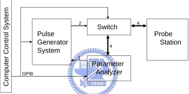
The multi stages measurement technique has been widely used in Non-volatile Memories (NVM) measurement systems, especially in the reliability researches, such as program/erase cycling process and stress/retention process. Fig. 2-1 shows this measurement system structure. A powerful parameter analyzer (e.g. Agilent 4156 series) can both offer and detect voltage/current signals precisely. A pulse generator (e.g. 8110 series) can give program/erase gate/drain voltage as short as micro second level. And a switch (e.g. Agilent 5250) together with the computer controlling system can provide the switching service between multi phases; that really saves a lot of time and gives a good way to avoid making possible experimentally mistakes. Because the operation of bias temperature instability (BTI) experiment (stress-measurement repeatedly) has similar setups compared with the reliability experiment of NVM, operating with same experiment system would be the best choice. Indeed, by this system structure, there are some mechanisms proposed for the BTI research, and the most famous one is reaction-diffusion (R-D) model which gives good explanations to the threshold voltage shifts of BTI-stress after second-level and will be introduced in chap3. But as the device-area scaling down and tunneling models established, engineers start to doubt that may trapped charge will also contribute to BTI? That’s really a question! According to tunneling models, a hole tunneling through a Å-level gate oxide only costs about few milli-second! For a conventional NVM measurement system, to detect threshold voltage shift down to millisecond level between multi phases is a difficult mission. Because there are lot’s of reasons to cost
time, such as[2.1-2]: z Switching delay
z Program delay (data storage/handling, machine initialization and parameter setup … etc.)
z Machinery delay (voltage slew rate … etc.) z Transmission line delay
z Resistors and parasitic capacitances delay
However, among above delays, the most important are the former three ones, which cost more than hundred of milliseconds. And, indeed, as Fig. 2-2 shows, the information lost below second level will tend to cause underestimating the degradation of current or threshold voltage shift, which probably caused by charge emissions, as shown in Fig. 2-3. On the other hand, the one of important benefits of fast switching transition monitor is that we can reduce much experiment time if we would like to extract the data in the same numbers of decades; that is, if we want to get six-order observation, for period equal to millisecond, we only pay 103 seconds, but for period equal to second, we have to cost 106 seconds!
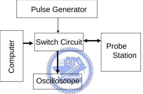
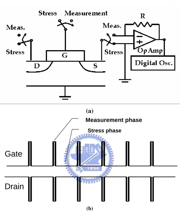
Based on the above ideas, we have to design a system that have the following properties:1.) This tool could avoid or minimize switching and machinery setup delay. And 2.) It also can avoid the delays cause by the computer controlling system. Fig 2-4 shows the system structure for BTI stress-measurement purpose. Since the oscilloscope only accept voltage signals inputs, a negative feed back circuit with OP-amp is required and the voltage signal amplitude translated from drain-current depends on the connecting resistor (Fig. 2-6-a) we used. The switches used for exchanging stress and measurement phases, of course, should fit 1.)’s requirement. Another thing that should be emphasized is that we observe the drain-current instead of threshold voltage for NBTI experiments. The reason is that, comparing with
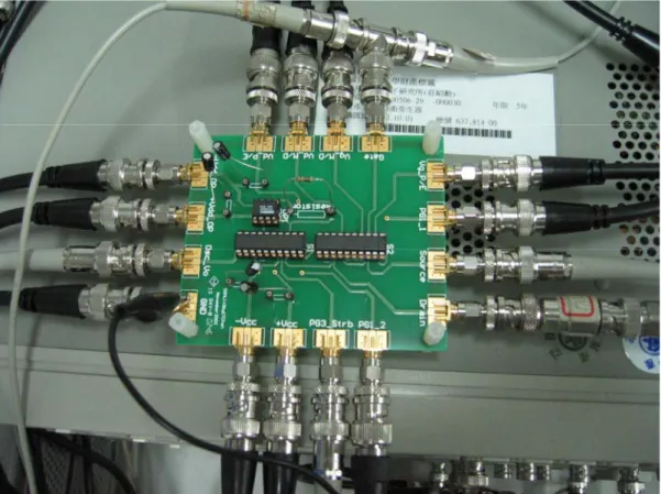
observation of threshold voltage, observation of drain-current is instant and this may reduce the amount of missing data during measurement. On the other hand, because we use a simple circuit instead of conventional large experiment system, the program and setup delay are automatically reduced. Fig. 2-5 is a photo of our circuit system. The performance of the switching time of this system is about 50 micro-second, which is about tens of thousand times shorter than conventional ones.
2.2 NBTI Experiment
For a pMOSFET, an NBTI experiment is performed with two phase measurement by the above circuit system. Fig. 2-6 illustrates the operation NBTI experiments. During stress phase, a greater negative gate voltage is applied while the other three terminals are connected to ground. During measurement phases, smaller voltage applies on the gate and drain side while source and bulk are grounded. Since the change between two phases is finished by switches, again, the switch delay must be emphasized; or, we will get an unreliable data.
Probe
Station
Switch
Parameter
Analyzer
Pulse
Generator
System
Comput
er C
o
nt
rol S
y
stem
4 4 1 2 GPIBFig. 2-2 Recovery transient in high-k NMOS [2.3]. As shown, significant amount ignored between micro-second level and second level.
Stress Phase-High Vg
(a)
Measurement Phase-Low Vg
(b)
Fig. 2-3 Energy band diagram during stress phase (a) and measurement phase (b). Charges de-trapping may happen during measurement phase.
Probe
Station
Switch Circuit
Pulse Generator
Oscilloscope
Computer
Fig. 2-4 The fast transient measurement system. Pulse generator offers the P/E voltages. By switch circuit, the drain-current signals are transferred to voltage signals and showed on the oscilloscope. The switch time is as short as tens of micro-seconds.
Fig. 2-5 The photo of the circuit system. The switch time can be minimized to micro-second.
(a)
Measurement phase Stress phaseGate
Drain
(b)Fig. 2-6 (a) Scheme of switch system operation. (b) Patterns for pMOSFET NBTI operation. The broaden edge sides represent the switch delay that may cause loss of information by a conventional experiment method and can be solved by fast transient
Chapter III
Negative Bias Temperature Instability Effects in Oxide pMOSFET
3.1 Studies of Negative Bias Temperature Instability
Since 1990, Negative Bias Temperature Instability (NBTI) Effect, which causes
d
I current degradation or threshold voltage shifts, arises engineer’s curiosity. After
years of efforts, a possible mechanism-Reaction and Diffusion Model, have been purposed. It states that only Hydrogen-related species are responsible for the degradation and recovery of the drain current; while in recent years, there are evidences that holes trapping and detrapping play an important role in recovery.
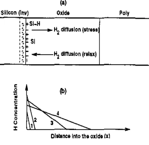
3.1.1 Reaction and Diffusion Model
According to [3.1-3], the NBTI effect can be related to the generation of the interface traps, which can be explained by Reaction and Diffusion model (R-D model). When a pMOSFET is biased in inversion, the holes in the inversion layer interact with Si-H bonds at the Si/oxide interface, which weakens the Si-H bonds. And finally leads to dissociation of H atoms together with the generation of interface traps (N ), it
just like a reversible chemical reaction (Fig. 3-1). The Reaction part can be represent by the following chemical equation:
f
r
k k
Si−H ←⎯⎯⎯⎯→ Si⋅ + −H relate species
Thus we can easily understand the following rate equation:
[
]
( )0 0 it f it r it H dN k N N k N N dt = − −Where N is the numbers of Si-H bonds initially, 0 NH( )0 is the N at H x=0, k f
and k represent the rate constant of forward and reverse reaction. r
the creation of N . By integrating standard hydrogen diffusion equation, the rate it
equation can be represented as below:
0 | 2 it H H x dN dN dN D dt dx dt δ = = +
Where δ is the interface thickness.
It is worth to comment that under this kind of NBTI measurement (conventional DC method), the variation of current can be well explained by interface traps N it
generation and recovery. During stress phase, N increases and the threshold voltage it
drops; while during recovery phase, due to the back diffusion of hydrogen atoms repair the broken Si-H bonds, N decreases, so that current increases with time. it
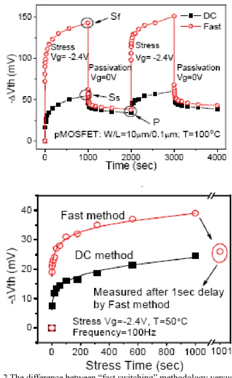
However, in recent years, researchers offer a new kind of idea [3.4-5] showing that with fast phase switching, we could find that the decrease of threshold voltage was underestimated by the DC method before (which delay about seconds order) (Fig. 3-2). They thought the recovery of threshold at the beginning is owing to the detrapping of holes rather than passivation of interface traps and gave a model of holes trapping and detrapping mechanisms to explain it. In this chapter, we will use the fast switching method which described in chapter two to see what will happen in the large and, especially, small devices.
3.2 Experiments 3.2.1 Experimental
The pMOSFET used in this work has a nitrided oxide thickness of 1.6nm and 2.0nm, a gate width from 0.2 mµ to 10 mµ , and a gate length from 0.12 mµ to 1 mµ . The devices are first subjected to a negative gate bias stress and “recover” in a smaller negative bias. In the “stress” phase, the inverted holes filling pre-existed traps and generates additional hole traps; while in the “recovery” phase, trapped holes escape
with thermal assistant tunneling. As described before, a conventional measurement causes some delay time due to the slow switching and we may lose lots of information. Fig. 3-3 shows the measurement pattern operated by a fast switching circuit which minimizes switching delay time to micro seconds. Owing to get more real time detections, we choose to observing drain current rather than threshold voltage shift.
3.2.2 Recovery in Large and Small Area Devices
The recovery transient current of large area devices (W L/ =10µm/1µm),
stressed individually in “strong” ( 3 , 100o , 500
g
V = − V C s ) and “weak”
( 3 , 100o , 2
g
V = − V C s) stress condition is shown in Fig. 3-4, with recovery gate
voltage is -0.3V. We can find that : 1.) Transient current is logarithmic time-dependent. 2.) The transient current slope increases with NBTI hardness. Furthermore, we have to notice that the time scale is as small as millisecond level. It implies that the conventional NBTI measurement method is underestimated seriously.
On the other hand, we apply the same stress conditions to the small devices (W L/ =0.4µm/ 0.18µm) and we discover the contrast between large and small
devices is remarkable. In the large devices, we observe a continuous, logarithmic dependence between current and time. While in the small devices, a discontinuous, step or stair-like current jumps was observed and shown in Fig. 3-5 and Fig. 3-6 for “weak” and “strong” stress condition. We believe that each of the jumps is due to the detrapping of a trapped hole in the oxide layer. A two dimensional simulation was performed, which fit the amplitude between two current jumps well (∆I Measurement Simulationd : 0.04µA: 0.03µA). In addition, firstly, the “strong” stress devices showed more current jumps than the “weak” stress one, implying that more trapped holes emitted due to more trapped charge density. Secondly, we can find
that the earlier emission current jumps have the potential of larger amplitude than the later ones, and will be explained in the later section. Thirdly, again, we have to notice the emission time of the first current jump (τ1), which is tens of millisecond and quite short than the conventional switching time of second level. That is, the conventional switching measurement methods may fail to discover or lose a lot of information in this experiment.
In order to establish the single charge emission model for oxide pMOSFET, we have to find relations between emission time τ and some dependent variables. Since we believe that τ is a function of temperature and gate voltages, we perform these results in Fig. 3-7 and Fig. 3-8. Fig. 3-7 shows the gate voltage dependence for τ1 andτ2, which are extracted by taking average of ten times measurements in the same device. Obviously, we can find that the charge emission time is positive related to recovery gate voltage, that is, the greater the gate voltage, the longer emission time. Fig. 3-8 shows the temperature dependence for charge emission time in 25℃, 50℃ and 75℃, respectively. Again, we see the positive relation between temperature and emission times. Or we may say that, the thermal energy helps the emission process of trapped holes. Additionally, we applied Arrhenius rate equation:
a E kT R=Ae− or ln Ea R C kT = −
We get the escape or detrapping activation energy is 0.5eV.
3.3 Results and Discussion
3.3.1 Single Charge Emission Model for Oxide pMOSFET
is τ0really a “stable” or “invariant” constant? From Fig. 3-7 and Fig. 3-8, it is not
hard to discover that τ0 is strongly depending on temperature and gate voltage. Also, with the helping of these two figures, we can try firstly to establish the model of charge emission and secondly to write down the possible tunneling time formula. Referring to Fig. 3-9, it illustrates the several possible detrapping paths: Path A) Trapped holes are excited to oxide valence band and then escape, Path B) Trapped holes escape toward gate direction and Path C) Trapped charges escape toward substrate direction. Before analyzing, we have already excluded the movement of charge particles, such as hydrogen cation or something else. If such charged particles are responsible for the recovery of drain current; the I will be dependent on the d
diffusion ability of charged particles. However, we can see from Fig. 3-5 or Fig. 3-6, that we only have a perfect step-like line and the drain current is quite stable during any jump. So that, it is nearly impossible to say that the current recovery is due to the diffusion of charged particles. Among three possible paths, first, we can easily exclude path A. Fig. 3-10 and Fig 3-11 shows the energy band diagram for stress and measurement modes, that is, the highest possible hole energy to oxide valence band is about 2eV. However, according to Fig. 3-8, the activation energy of holes detrapping is only about 0.5eV. The activation energy of detrapping, 0.5eV, is much smaller than trap energy 2eV. Between path B and path C, which just the opposite direction, can be picked up by Fig. 3-7. It shows the dependence between gate voltage and emission time. The greater gate voltage is, the greater negative electric field applies along the gate-substrate direction. Thus, holes are easier to tunnel out to gate side. But, what we observed is the longer emission time when gate voltage goes more negative. It implies that path C is the correct one; otherwise, path B, will give a negative relation to voltage- time dependence. In addition, Fig. 3-5 or Fig. 3-6 will also give an indirect evidence to the result. From Fig. 3-5 or Fig. 3-6, one of the conclusions is that “the
earlier detrapping amplitudes tend to be larger than the latter ones.” If we neglect the influence of self voltage adjustments, we have the following dependence:
Q I S V S C ∆ ∆ ∝ ∆ = ox trap to gate C x − − ∈ =
So that, we can get:
trap to gate ox Q I S∆ x − − ∆ ∝ ∈ … (1) With the helping of fundamental WKB tunneling time expression:
( )
0exp x
τ τ= α … (2)
For path B, the earlier detrapping holes have nearer detrapping pathway to gate or smallerxtrap to gate− − , so the earlier current jumps should contribute to smaller amplitudes.
On the other hands, for path C, the earlier detrapping holes have nearer detrapping pathway to substrate or largerxtrap to gate− − , so the earlier current jumps should give
larger amplitudes. Obviously, path C is correct but path B not.
Finally, we can give a possible formula for the tunneling time depending on the temperature, voltage relation and energy band diagram together with the mechanism discussed above. For the th
i hole tunneling time may be given as follow[3.6-7]:
(
)
1(
)
1 exp a exp i v v ox i E N f x kT τ =⎡⎣ − σ⎤⎦− ⎛⎜ ⎞⎟ α ⎝ ⎠ Where * 2 2 t ox m E α =h and σ is cross-section in meaning. N is the effective hole v
density of states in the Si valence band; f represents the Fermi-Dirac distribution v
function in the substrate with the identical energy level to the hole traps. That is,
(
1)
v v
N − f means the available states for holes detrapping out and that is the reason
emission time. As the gate voltage goes smaller or below the threshold voltage, f v
approached to zero. It causes the gate-voltage dependence tends to disappear, as shown in Fig. 3-8.
3.3.2 Oxide Trap Density
The oxide trap density (N ) can be evaluated through the proposed analytical t
model. Referring to Fig. 3-9 and by comparing:
(
)
1(
)
1 v 1 v exp a exp ox 1 E N f x kT τ =⎡⎣ − σ⎤⎦− ⎛⎜ ⎞⎟ α ⎝ ⎠(
)
1(
)
2 v 1 v exp a exp ox 2 E N f x kT τ =⎡⎣ − σ⎤⎦− ⎛⎜ ⎞⎟ α ⎝ ⎠The energy levels between two traps are small enough. Divide the above two equations, we obtain
(
)
2 2 1 1 exp ox x x τ α τ = ⎡⎣ − ⎤⎦ … (3)And the oxide traps have a uniform distribution along the oxide thickness, the oxide trap density can be approximated to,
(
2 1)
2 1 1 ln ox t N WL x x WL α τ τ = = − ⎛ ⎞ ⎜ ⎟ ⎝ ⎠ … (4)From Fig. 3-12, if the above two assumptions are not far from the truth, equation (3) predicts the ratio of first and second emission time only depend on the distance between two traps, and are independent of gate voltage.
The extracted oxide trap density in the “weak stress” device is about 3.5*1010cm-2 and that is quite reasonable. By using this trap density to modeling large area device recovery in Fig. 3-4, an excellent fit to the measured result is obtained.
3.3.3 Modeling of Recovery Transient in Large Area Devices
extend to large area devices. In a large area device, the oxide charge detrapping rate is
( )
,( )
,0 exp( )
t Q x t Q x x τ ⎡ ⎤ = ⎢− ⎥ ⎣ ⎦where Q x t
( )
, =qNt( )
x t, is the time dependent trapped charge density in oxide and( )
xτ is described in section 3.3.1. Thus the oxide trapped charge induced threshold voltage shift can be written as the summation effect of individual trapped oxide charges
( )
( )
( )
(
)
(
)
,0 1 exp , t i i i t i i i ox ox i t qN x Q x t V t C x t x τ ⎡ ⎛ ⎞⎤ − − ⎢ ⎜ ⎟⎥ ∆ ⎣ ⎝ ⎠⎦ ∆ = = ∈ −∑
∑
…(5)where C x
( )
i is the corresponding capacitance for trapped charges located at x ifrom the gate-oxide/substrate interface, ∈ is the permittivity of the gate-oxide and ox
ox
t is the physical thickness of the gate oxide. If the amount of traps in large area
device is numerous, we can represent (5) as integration form.
( )
t( ) (
,0)
1 exp( )
t ox ox qN x t V t t x dx x τ ⎧ ⎡ ⎤⎫ ⎪ ⎪ ∆ = − ⎨ − ⎢− ⎥⎬ ∈ ⎪⎩ ⎣ ⎦⎪⎭∫
…(6) with the definition of τ( )
x in small area devices, and the dependence of x is( )
(
)
(
)
(
)
0
1 0
.
exp 1 exp a exp
ox v v ox indep of x E x x N f x kT τ τ =τ α =⎡⎣ − σ⎤⎦− ⎛⎜ ⎞⎟ α ⎝ ⎠ 14444244443 so that, (6) becomes
( )
( ) (
)
(
)
0 ,0 1 exp exp t t ox ox ox qN x t V t t x α x dx τ ⎧ ⎡ ⎤⎫ ⎪ ⎪ ∆ = − ⎨ − ⎢− − ⎥⎬ ∈ ⎪⎩ ⎣ ⎦⎪⎭∫
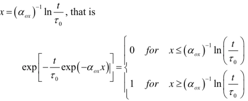
…(7)For the integration of double exponential term in (7), we can reference the similar method in [3.8], approximate this term as a step function abruptly around
( )
1 0 ln ox t x α τ − = , that is(
)
( )
( )
1 0 1 0 0 0 ln exp exp 1 ln ox ox ox t for x t x t for x α τ α τ α τ − − ⎧ ⎛ ⎞ ≤ ⎪ ⎜ ⎟ ⎡− − ⎤ ⎪ ⎝ ⎠ = ⎨ ⎢ ⎥ ⎛ ⎞ ⎣ ⎦ ⎪ ≥ ⎜ ⎟ ⎪ ⎝ ⎠ ⎩Fig. 3-13 shows this property. This approximation gives a picture that:after time t, electrons with emission times shorter than t are de-trapped out and others are remain trapped. Thus, with the assumption of double exponential (7) can be further simplified as
( )
1( ) (
)
0 ln 0 ,0 ox t t t ox ox qN x V t α τ t x dx − ∆ = − ∈∫
…(8) Again, if oxide traps are uniformly distribution along gate-substrate direction, then oxide trapped charge density can be drawn out from the integration sign. And we get( )
1(
)
0 1 0 ln 0 ln almost invarient 0 0 1 2 ln ox ox eff t t t ox ox t t ox ox X t eff ox ox qN V t t x dx qN x t x qN X t α τ α τ α τ − − ∆ = − ∈ ⎛ ⎞ = ⎜ − ⎟ ∈ ⎝ ⎠ = ∈∫
14243 …(9)Thus, the corresponding recovery drain current can be represent as follow:
( )
( )
t eff ln t ox ox qSN X I t S V t t α ∆ = ∆ ∝ ∈Now, we can explain what we observed in large area devices as Fig. 3-4. Firstly, the logarithmic dependence is as what we prediction; and secondly, the strong stress condition induced larger slope is correspond to the larger oxide trapped charge density. Thus, we have well simulated recovery transient in good agreement with experiment also shown in Fig. 3-4. Table 3-1 is the parameter table.
3.4 Summary
A novel transient measurement technique is proposed to characterize oxide traps in pMOSFETs. The quantized feature in recovery current evolution due to single charge detrapping is observed in a small area device. A SRH-like thermally-assisted tunneling model [3.6-7] for charge emission is established. This model can well explain the gate-voltage and temperature dependence of the emission time; also, the oxide trapped charge density can be extracted from emission times. The extension from small area devices to large area devices is also performed by the well fitted simulation.
Fig. 3-1 Graphics of Reaction-Diffusion models for NBTI
Fig. 3-2 The difference between “fast switching” methodology versus conventional methodology and the missing information is quite significant.
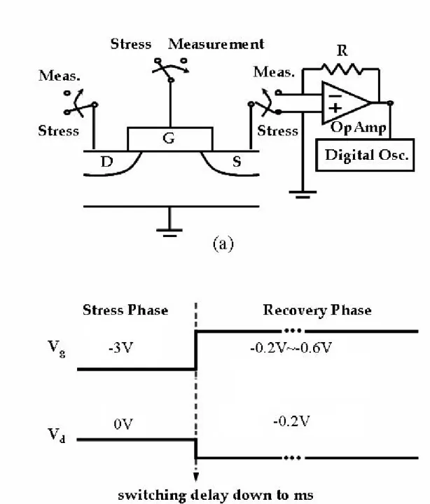
Fig. 3-3 (a) Schematic diagram for PBTI recovery transient measurement. (b) The waveforms applied to the gate and drain during stress and recovery phases.
Fig. 3-4 Recovery transient right after NBTI stress is demonstrated to be significant. Stress condition is Vg=-3V at 100C for 2s (“weak”) and for 500s (“strong”). The recovery follows a logarithmic time dependence, and the slope grows abrupt with a harder stress. Also appended is the simulation result which is in good
Fig. 3-5 A typical step-like “quantum jump” observed in channel current during NBTI recovery enables explicit definition of trap characteristic times, denoted in the figure as t1 and t2. Each jump corresponds to a single trapped hole emission from the oxide.
Fig. 3-6 Compared to a “weak stress” condition (Vg= -3V, 2s) in which only two quantum jumps are measured, a post “strong stress” (Vg= -3V, 300s) recovery has five jumps in the same time span.
10
-2
C
h
ar
ge
Em
is
si
on
T
im
e (
s)
Recovery V
g
-V
t
(-V)
0.1
0.2
0.3
0.4
10
-1
10
0
<
τ
2
>
<
τ
1
>
10
-2
C
h
ar
ge
Em
is
si
on
T
im
e (
s)
Recovery V
g
-V
t
(-V)
0.1
0.2
0.3
0.4
10
-1
10
0
<
τ
2
>
<
τ
1
>
Fig. 3-7 Recovery Vg dependence of trapped hole emission times, t1 and t2. Longer emission times for larger Vg’s exclude charge escape into gate electrode. Note that t2-to-t1 ratio remains constant.
1000/T (K
-1
)
2.8
3.0
3.2
3.4
<
τ
1
> (s)
E
a
=0.5eV
T
ox
=22A
0.01
0.1
1000/T (K
-1
)
2.8
3.0
3.2
3.4
<
τ
1
> (s)
E
a
=0.5eV
T
ox
=22A
0.01
0.1
Path A
Path B
Path C
Gate
Vg~-3V
Substrate
Vb=0V
E
fTrapping
Holes
Gate
Vg=-0.2~-0.6V
Substrate
Vb=0V
E
f(Rec.)
E
f(stre.)
Hole Detrapping
Fig. 3-11, Energy band diagram for measurement (recovery) mode. The hole-traps between recovery and stress Fermi level will de-trap to substrate and gives stair-like
Recovery V
g
-V
t
(-V)
0.05
0.25
0.35
1
10
100
τ
1
τ
2
Ox
ide Trap
De
n
si
ty
(c
m
-2
)
10
1110
1010
90.15
Average N
ox=3.5*10
10cm
-2Recovery V
g
-V
t
(-V)
0.05
0.25
0.35
1
10
100
τ
1
τ
2
τ
1
τ
2
Ox
ide Trap
De
n
si
ty
(c
m
-2
)
10
1110
1010
90.15
Average N
ox=3.5*10
10cm
-2Fig.3-12 Vg dependence of t2/t1 and the corresponding oxide trap density. Note that t2/t1, remains unchanged for all recovery Vg. Ten devices were measured to take
Sub
stra
te to
Ga
te
Tim
e(s
)
F(
x
,t)
1
0
1
Fig. 3-13 Double exponential function of distance and time. It shows the abrupt property. Thus we can reduce the integral to a simple form.
parameter value unit reference/T-depend.
Nv 1.45E+25 m^-3 Sze (Appendix H), proportional to T^1.5 σ 1.8E-18 m^2 value:fitting parameter such that t0=1e-3 m*h,ox 0.42 m0
Ea 0.5 eV measured, low Vg, T=25C~75C (higher for T>100C) S 0.05 V/dec. Measured
Tox 2.2E-09 m
Id0 1.16E-06 A measured, full-recovery Id
Table 3-1 Fitting parameters for NBTI effect in large area devices as shown in Fig 3-4.
Chapter IV
The Single Charge Effects on Devices Length
4.1 Introduction
As the device dimensions continues to shrink in the next generation of MOS technology, the effect of an individual defect on device performance becomes more pronounced. In the previous chapter, an obvious difference of BTI between large and small area devices is shown. Recovery drain current in the large area devices shows logarithmic time dependence, while in the small area ones, it gives multi-level recovery current jumps. What the single charge effects will be as the devices keep scaling down? In the chapter, we will give an experimental relation between current jump amplitude and gate length. The length effects in other devices and a simple comparison to the Random Telegraph Signals (RTS) will also be given.
4.2 Current Jump Amplitude versus Channel Length Effect
We made some experiments to study the relation between current jump amplitudes and channel length. The operation is two-phase measurement, stress/recovery, as described in chapter III. The lengths of devices are from 0.24 mµ to 0.08 mµ . Fig. 4-1 shows the current jumps of oxide pMOSFET in different length. Obviously, the current jump in a longer channel length is smaller than in a shorter one. Fig. 4-2 shows this trend. The similar trend is also obtained in high-k nMOSFET devices [4.1] as shown in Fig. 4-3. That is, this is a question that can’t be avoided in all kinds of small-area devices in the future. The possible reason may be that:As the channel length shrinking, the single electron effected length percentage increases. So that, the current difference (∆Id) caused by a single charge in a smaller device will be
more and more significant.
4.3 The Channel-Length Dependence in RTS
The RTS’s in a small area MOSFET, characterized by discrete changes of drain current as a function of time, is believed to be due to the trapping/detrapping events caused by an individual interface defect near Si/SiO2 interface. Compared with the
single charge emission model in chapter III, they have some similar points, such as both involving with charge detrapping from a defect. Thus, they may have certain properties in common. In recent ten years, RTS’s theory has been widely studied. The length dependence also been proposed in [4.2] [4.3]. In our recent research, the length dependence of RTS in different pocket doping devices is shown in Fig. 4-4. Both show that the RTS amplitude increase with length decreasing. Additionally, owing to preventing punch-through occur, higher concentration pocket implantation is required. Unfortunately, this non-uniform threshold along channel length direction will also enhance the drain current fluctuation. The heavier doped pocket of shorter length devices gives the most serious variation in drain current.
4.4 Summary
We have shown by experiments and studies that both the NBTI recovery current jump amplitudes and RTS amplitudes tend to increase as we scale down the device dimensions. When a non-uniform distribution of threshold voltages exists along the channel, which is more likely to exist in a deep submicron device, the drain current fluctuations are enhanced, with a dominant contribution from the region of a higher threshold voltage, such as caused from pocket implantation. Both give the information of the reliability issue in the future small area devices.
0.1
0.2
0.3
10
20
30
40
50
60
Low Pocket
High Pocket
Av
er
ag
e
∆
I
d
(n
A)
L
g
(
µm)
0.1
0.2
0.3
10
20
30
40
50
60
Low Pocket
High Pocket
Av
er
ag
e
∆
I
d
(n
A)
L
g
(
µm)
Fig. 4-4 Length effect on the average RTN amplitude. Short Lg and/or high pocket give
Chapter V
Conclusion
We proposed a computer-automated transient technique with a switching delay down to microseconds to investigate NBTI recovery. This technique allows to measure individual hole de-trapping times directly in NBTI recovery. Based on the measured temperature and Vg dependence of single hole detrapping time, trapped hole
emission through thermally-assisted-tunneling has been shown to be a dominant mechanism for the fast transient of NBTI recovery. Additionally, the activation energy for charge emission is about 0.5eV for an oxide pMOSFET. Trap density can also be evaluated simply by measuring the ratio of the first two charge emission times in small-area devices.
On the other hand, the dependence of the current jump amplitude on gate length is measured. A shorter gate length device has a larger current jump. This result is similar with the RTS theory, implying that the impact of a trapped hole spreads over the entire channel. And this phenomenon will be more obvious in the coming generations.
Reference
Chapter 1
[1.1] “International Technology Roadmap for Semiconductors 2005 Edition, Process Integration, Devices, and Structures” pp. 47-53
http://www.itrs.net/Links/2005ITRS/PIDS2005.pdf
Chapter 2
[2.1] “HP 5250A Low Leakage switch Mainframe - User’s Guide”,
Hewlett-Packard Company, page A-7, 1997
[2.2] “HP4155A Semiconductor Parameter Analyzer User’s Dictionary Reference”, Hewlett-Packard Company, chapter 9
[2.3] C.T. Chan, “Bias Temperature Instability in COMSFETs with Advanced Gate Dielectrics” pp. 23, 2006
Chapter 3
[3.1] M.A. Alam, “A Critical Examination of the Mechanics of Dynamic NBTI for PMOSFETs” IEDM. Tech. Dig., pp. 14.4.1-14.4.4, 2003
[3.2] S. Mahapatra, M. A. Alam, P. Bharath Kumar, T. R. Dalei and D. Saha, “Mechanism of Negative Bias Temperature Instability in CMOS Devices: Degradation, Recovery and Impact of Nitrogen” IEDM Tech. Dig., pp. 105-108, 2004
[3.3] Shigeo Ogawa, Masakazu Shimaya, and Noboru Shiono, “Interface-trap generation at ultrathin SiO2 (4-6nm)-Si interfaces during negative-bias
temperature aging”, J. Appl. Phys., Vol. 77, pp. 1137-1148, 1995
[3.4] T. Yang, M. F. Li, C. Shen, C.H. Ang, Chunxiang Zhu, Y. C. Yeo, G. Samudra, Subhash C. Rustagi, M. B. Yu, and D. L. Kwong, “Fast and Slow Dynamic NBTI components in p-MOSFET with SiON dielectric and their impact on device life-time and circuit application”, Symposium on VLSI Tech.
Dig. of Technical Papers, pp. 92-93, 2005
[3.5] V. Huard and M. Denais, “Hole Trapping Effect on Methodology for DC and AC Negative Bias Temperature Instability Measurements in pMOS transistors”, 42nd Annual IRPS, pp. 40-45, 2004
[3.6] Nasyrov, K.A.; Gritsenko, V.A.; Kim, M.K.; Chae, H.S.; Chae, S.D.; Ryu, W.I.; Sok, J.H.; Lee, J.-W.; Kim, B.M, “Charge transport mechanism in metal-nitride-oxide-silicon structures”, IEEE EDL., vol. 23, issue 6, pp. 336-338, 2002
[3.7] R. R. Hearing and E. N. Adams, “Theory and application of thermally stimulated currents in photoconductors,” Phys. Rev., vol. 117, pp. 451-454, 1960
[3.8] Tahui Wang, Lu-Ping Chiang, Nian-Kai Zous, Tse-En Chang, and Chimoon Huang, “Characterization of Various Stress-Induced Oxide Traps in
MOSFET’s by Using a Subthreshold Transient Current Technique,” IEEE
Transactions on Electron Devices, vol. 45, NO. 8, 1998
Chapter 4
[4.1] C. T. Chan, C. T. Tang, C. H. Kuo, H. C. Ma, C. W. Tsai, H. C.-H Wang, M. H. Chi, and Tahui Wang, “ Single-Electron Emission of Traps in HfSiON as High-k Gate Dielectric for MOSFETs,” Proc. Int. Reliab. Phys. Symp.
(IRPS), pp. 41-44, San Jose, U.S.A., 2005
[4.2] Ming-Horn Tsai, T. P. Ma, and Terence B. Hook, “Channel Length
Dependence of random Telegraph Signal in Sub-Micron MOSFET’s,” IEEE
Electron Device Letters, vol. 15, no. 12, pp. 504-506, 1994
[4.3] Ming-Horn Tsai and Tso-Ping Ma, “The Impact of Device Scaling on the
Current Fluctuations in MOSFET’s” IEEE Transactions on Electron Devices, vol. 41, no. 11, pp. 2061-2067, 1994
![Fig. 2-2 Recovery transient in high-k NMOS [2.3]. As shown, significant amount ignored between micro-second level and second level](https://thumb-ap.123doks.com/thumbv2/9libinfo/8241741.171351/18.892.153.753.380.765/recovery-transient-nmos-shown-significant-ignored-second-second.webp)