行政院國家科學委員會專題研究計畫 期中進度報告
半導體量子環和其在自旋電子元件之應用(2/3)
期中進度報告(精簡版)
計 畫 類 別 : 個別型 計 畫 編 號 : NSC 94-2215-E-009-010- 執 行 期 間 : 94 年 08 月 01 日至 95 年 07 月 31 日 執 行 單 位 : 國立交通大學電子工程學系及電子研究所 計 畫 主 持 人 : 李建平 處 理 方 式 : 本計畫可公開查詢中 華 民 國 96 年 11 月 01 日
行政院國家科學委員會補助專題研究計畫
□成果報告 ■
期中進度報告
半導體量子環及其在自旋電子元件之應用(2/3)
計畫類別:■個別型計畫 □ 整合型計畫
計畫編號:NSC 94-2215-E-009-010-
執行期間:94 年 8 月 1 日至 95 年 7 月 31 日
計畫主持人:
李建平
共同主持人:
計畫參與人員:
李秉奇、凌鴻緒
成果報告類型(依經費核定清單規定繳交):■精簡報告 □完整報告
本成果報告包括以下應繳交之附件:
□赴國外出差或研習心得報告一份
□赴大陸地區出差或研習心得報告一份
□出席國際學術會議心得報告及發表之論文各一份
□國際合作研究計畫國外研究報告書一份
處理方式:除產學合作研究計畫、提升產業技術及人才培育研究計畫、
列管計畫及下列情形者外,得立即公開查詢
□涉及專利或其他智慧財產權,□一年□二年後可公開查
詢
執行單位:
國立交通大學電子工程學系
中 華 民 國 95 年 10 月 31 日
報告內容:
(1) 前言:
The nanoscale quantum confined ring structures (quantum rings) have attracted efforts in research for decades due to their unique excitation properties [1-12] and potential in the implementation of spintronic technology. For a semiconductor quantum ring (QR) structure, it is predicted that its ring shape potential can trap single magnetic flux and thus has large permeability under certain magnetic fields. So the semiconductor QRs possess the potential to serve as simulated magnetic materials for the part of memory device integrated in single chip.
Within the methods of fabricating semiconductor QRs, self-assembled growth using molecular beam epitaxy (MBE) technology might be the most promising one [13-20]. Because of the fabrication within single growth run without necessity of process, self-assembled QRs eliminate severe interface defect and thus have high quantum efficiency. This high quantum efficiency permits good opportunity to meet the requirement of device application.
For the formation of InAs QRs in GaAs matrix, the capping and annealing procedure with a thin Ga(Al)As layer deposited on top of the InAs quantum dots (QDs) is commonly used. The partially capped QDs allow outward migration of In atoms from the tips of the dots to the surrounding region during annealing. Quantum rings are therefore formed because of the depletion of In at the center of the dots.
The mechanisms of the outward migration of In atoms from the QDs have been attributed to (1) a higher In surface mobility (compared to Ga) at the annealing temperature that causes the outward “diffusion” of In atoms from the uncovered InAs dots [13, 14] and (2) the instability at the interface between the exposed InAs droplets and the surrounding solid GaAs providing an outward driving force for the uncovered InAs [14, 21]. Therefore, the whole process is quite complicated. The surface migration (referred to as diffusion in ref. 14) depends on the temperature and the duration of annealing, and the imbalanced surface tension at the solid-liquid interface depends on the shape of the InAs dots and the cap layer thickness.
(2)
研究方法:
In this project, we have investigated the evolution of InAs quantum ring formation. By controlling the extent of outward migration of In material, we were able to obtain nanostructures at different stages in QR formation. The dependence of shape change on certain growth parameters also provided us more insights into the mechanisms of ring formation. The samples used in this study were grown on GaAs (001) substrates by a Varian GEN II solid-source MBE system with a valved cracker source of Arsenic. A single InAs QD or QR layer was sandwiched between two GaAs barrier layers. An additional InAs layer with the same growth condition as the embedded InAs layer was grown on the surface for the purpose of AFM measurement. Except the region near the InAs layer, the GaAs barrier layers were grown at 590℃ for better quality epi-layers. The detailed growth procedure of active layers for respective samples will be mentioned in the next section.
The surface morphologies of our samples were characterized by a Digital-Instrument-D3100 AFM using the tapping mode. The emission spectra of the QDs and QRs were measured by photoluminescence (PL) spectroscopy. The samples were photo-excited by an Argon ion laser with the 514.5 nm line and were mounted in a close-cycled Helium cryostat for low temperature measurement.
(3) 結果與討論:
I. Effect of annealing temperature and dot size on the ring formation
Three samples (I, II and III) were prepared to investigate the effect of annealing temperature on quantum ring formation. They contain the same growth parameters of initial QDs but with different capping techniques to tailor the final structures in active layers. The initial QDs were formed by depositing 2.6MLs of InAs with a growth rate of 0.055 μm/hr and a growth temperature of 520℃ under As2 atmosphere. For sample I, after the QD growth, GaAs with 1 μm/hr growth rate was continuously grown to entirely cap the dots. No additional annealing step was used. But for sample II (III), after the dot growth was finished, the substrate temperature was ramped down rapidly to 450℃ (470℃) for the following capping and annealing process: a thin GaAs layer of 2.5 nm with 1 μm/hr growth rate was deposited to partially cap the dots and then a 50 sec interruption under As2 flux was performed at the same temperature for annealing. Finally, the GaAs barrier layer with 1 μm/hr growth rate was grown to complete the growth process. Note that this high growth rate for GaAs barrier was needed to minimize the deformation of the morphology of the as grown structure.
Their AFM images and the corresponding surface profiles of the individual dots or rings are shown in Fig. 1. We can see very clearly that after the capping and annealing process, the shape of the QDs was changed dramatically.
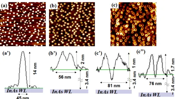
FIG. 1. The 1 x 1 um2 AFM surface images of (a) sample I (quantum dots), (b) sample II (quantum volcanos), and (c) sample III (quantum rings), and the representative surface profiles of individual structure in each sample. (a’), (b’), and (c’) represent the QR evolution from the group of large dots but (c’’) represents the final ring structure coming from smaller dots.
The original QDs, shown in Fig. 1(a) and (a’), changed to a volcano-like structure (sample II or Fig. 1(b) and (b’)) or a ring structure (sample III or Fig.1 (c) and (c’)) depending on the annealing temperature. At a lower capping and annealing temperature of 450℃, the outward migration of In atoms from the uncovered top of each dot left behind a volcano shaped structure as shown in Fig. 1(b’). When the capping and annealing temperature was raised to 470℃, more In atoms moved out of the dot leaving behind a deep
hole in the center depleted of InAs. In this case, a complete ring was formed. It should be mentioned that the surface profiles shown in Fig. 1 have different elevations, or height references. In sample I, with the dot profile shown in Fig. 1(a’), the QD stands on the wetting layer and the whole dot is visible. For samples II and III, however, the base height is elevated because of the cap layer coverage. Although the amount of GaAs deposited for the cap layer was 2.5nm, the actual thickness of the cap layer was estimated to be ~3.4nm due to the presence of the QDs, whose tips were not covered (Based on the size and the density of the QDs, 26% of the surface was covered by the dots in the QD layer). So for these two samples (II and III), a large portion of the InAs volcanos and rings lies below the surface of the cap layer. The actual height of the volcano shown in Fig. 1(b’) is 5.4 nm measured from the surface of the wetting layer and the height of the ring shown in Fig. 1(c’) is 4.4 nm.
If we look very closely at the surface image of sample I shown in Fig. 1(a), two groups of dots with different sizes are seen. Such bimodal size distribution is quite common in self-assembled QD growth. It is because that at a given growth condition, there is an optimum QD size and the number of nucleation sites. When the optimum size is reached, further deposition of In atoms will result in new nucleation and new dots. So the larger dots are the ones with the optimum size and the smaller ones are from later nucleations [14]. The surface profile of a typical larger size dot is shown in Fig. 1(a’). The height was around 14 nm and the base diameter was around 45 nm. For the smaller size dots, the typical height was 9 nm and the base diameter was 38 nm (not shown here). Now as these dots are covered by a thin cap layer, the uncovered portion of the dots is different depending on the size of the dots. Obviously the larger ones have a larger portion exposed and the smaller ones have a smaller portion exposed. When the samples are annealed, these two types of dots evolve into rings differently. A closer look at Fig. 1(b), which underwent 450℃ capping and annealing, indeed reveals two groups of dots, one with a small depression at the center and the other without. Fig. 1(c) of sample III, annealed at a higher temperature of 470℃ also shows two groups of rings with two different sizes.
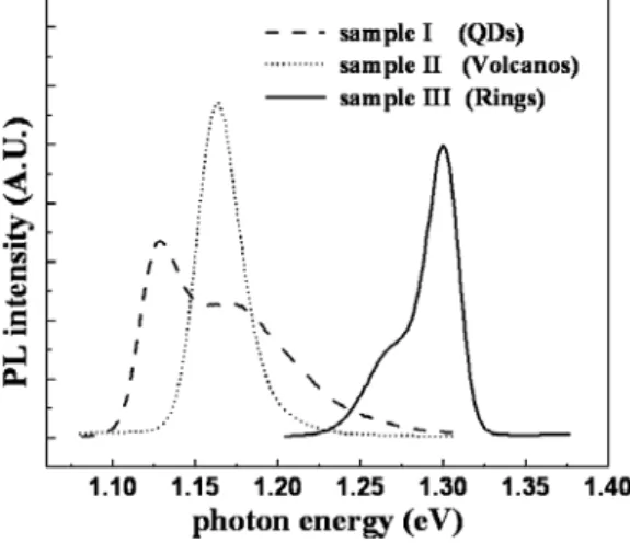
The PL emission spectra of the three samples are shown in Fig. 2. The excitation power used was purposely kept low to ensure only ground state emission is allowed. The bimodal
FIG. 2. The photoluminescence spectra of sample I to III under low excitation power (~1 W/cm2) at 13K.
distribution of the QDs in sample I, which was not annealed, is clearly seen with two emission peaks. After annealing at 450℃, the emission peak of sample II, shifts to a higher energy. Although it appears to be only a single peak, a careful fitting with Gaussian curves reveals there are actually two Gaussian distributions, a higher sharp peak at 1.163 eV with a FWHM of 27 meV and a lower broad peak at 1.176 eV with a FWHM of 52 meV. We
attribute the larger peak to the emission from the nano-volcanoes, which were evolved from the larger QDs. The shift in energy is readily understood because the height of the dots has been reduced as the nano volcanoes were formed (see Fig. 1(a’) and (b’)). The smaller peak was from the smaller dots. Because the emission wavelength of this peak is almost the same as that of the smaller dots in sample I, it is most likely that there has not been any change in the shape of the dots. The inability to change shape suggests that their tips were not exposed but instead covered by the GaAs layer during the annealing step. The reason for the coverage is probably due to the poor mobility of the deposited Ga adatoms at 450℃.
Further shift in emission peak to higher energy is observed for sample III, which was annealed at 470℃, due to further reduction in the height of the dots as rings are formed. Again two peaks are seen. The larger peak, at 1.301 eV, is originated from the rings evolved from the group of QDs with a larger size. The shoulder peak at a lower energy of 1.276 eV comes from another group of rings that are evolved from the original smaller QDs. These small dots, which were unchanged after 450℃ annealing, now have also changed to ring structures. The higher capping/annealing temperature causes the tips of the smaller dots also exposed because of the increased surface mobility of Ga atoms. Because a less amount of InAs is removed from the tip, the shift in energy of the emission peak is less than that of the larger rings. The surface profiles of these two kinds of rings are shown in Fig. 1(c’) and (c’’). The larger rings, which are originated from the larger dots, have a very deep hole at the center. The height is about 4.4 nm and the outer diameter of the rim is around 81 nm (Fig. 1(c’)). Comparing to those formed after 450℃ annealing, the volcano shaped structure has turned into a ring structure. For the rings that were originated from the smaller dots, the center hole is not as deep and the base is not as wide as the larger rings but the rim is higher (Fig. 1(c’’)). So clearly, the ring formation is at an earlier stage comparing to the larger ones. In other words, the smaller dots, after they are partially capped have smaller driving force for shape transformation than the larger QDs. As will be described in the following, this can be explained by the difference in the degree of surface tension imbalance for the different size dots as they are partially covered.
II. Effect of cap layer thickness on ring formation and the formation mechanism
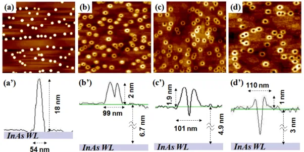
As described above, the difference in the amount of cap layer coverage for the QDs with different sizes causes difference in the final ring structure. So to get a better picture of the effect of cap layer on the ring formation, we have also prepared another group of QD samples (IV, V, VI and VII). In this group of samples, QDs with larger sizes were grown. 3.2MLs of InAs were deposited at a higher growth temperature of 540℃ and a lower growth rate of 0.033 μm/hr. Such growth condition also gave a better size uniformity for the QDs. In sample IV, the continuous capping of GaAs at 1 μm/hr was used for the QD reference. In samples V to VII, the partial-capping and annealing process was used for the QR formation. The GaAs cap layers were deposited at 505℃ and had thicknesses of 5.5 nm, 4 nm and 2.5 nm for samples V, VI and VII, respectively. Following the deposition of the cap layer, the samples underwent 50sec annealing at the same temperature of 505℃.
The AFM images of these samples and the surface profiles of the representative individual quantum structures are shown in Fig. 3. As shown in these pictures, the QDs (Fig. 3(a) and (a’)) again transformed via volcanos (Fig. 3(b) and (b’)) to rings (Fig. 3(c), (c’), (d) and (d’)) after the capping and annealing process. However, this time the factor that determines the final shape of the ring structure is not the temperature but the cap layer
thickness. The amount of In that migrates out from the center portion of the dots depends on the amount of coverage of the cap layer.
FIG. 3. The 1x1 um2 AFM surface images of (a) sample IV (quantum dots), (b) sample V (quantum volcanos), (c) sample VI (quantum rings), and (d) sample VII (quantum rings), and the representative surface profiles of individual structure in each sample.
In sample V, which had a thicker cap-layer of 5.5 nm, the QDs turned into volcano-like structures with the center crater about 1.4 nm deep. The rim of the volcano was 2 nm above the GaAs cap, which was ~6.7 nm thick (based on 5.5nm deposition and 18% coverage of the surface by the initial QDs). So the height of the InAs volcano was about 8.7 nm, which is a great reduction from the original 18 nm height for the QDs. The InAs material that moved from the top of the dots spread out to the adjacent area above the GaAs cap. The base of the volcano that rose above the GaAs surface was widened to 99 nm. We need to bear in mind, however, the base of the volcano bottom underneath the cap layer should be still the same as that of the original QD. Judging from the AFM picture, this volcano structure is still far from a ring. However, for sample VII, which had a thinner cap layer of 2.5 nm, the final structure had a very deep hole with the In atoms almost totally depleted (see Fig. 3(d’)). The rim of the ring, however, was only about 1 nm above the cap layer. In other words most of the ring was buried below the GaAs cap, which was about 3 nm thick. The outer diameter of the rim reached 110 nm, which is much wider than the original base diameter of the QD.
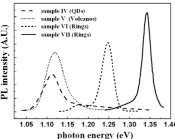
FIG. 4. The photoluminescence spectra of sample IV to VII under low excitation power (~1 W/cm2) at 13K
primary peak is seen for all the samples. Because of the growth condition chosen, we were able to get only one dominant size for dots. The emission peak continues to shift to higher energies as quantum rings are evolved from the original QDs due to the reduction of the height. Moreover, the quantum ring formation is accompanied by a peak width shrinkage, which can be observed clearly from Fig. 4. The FWHM of the emission peak from the QDs decreases dramatically from 50 meV to 23 meV after the dots are transformed to QRs. This is attributed to a better uniformity in the height of the rings after annealing. Since the thickness of the cap layer should be very uniform, the fluctuation of the height of the original dots results in different exposed top areas. Subsequent annealing and the outward migration of InAs will tend to smooth out the original height fluctuation and cause the height of the final structure more uniform.
Since the QD sizes are the same for all the samples discussed here, the sample with a thicker cap layer will have a less amount of the exposed portion that can move outward upon annealing. Not only that, the migration of the In atoms from the tops of the QDs depends on the imbalance of the surface tension at the interface between the cap layer and the QD droplet. Based on this so called dewetting model [13], it is not hard to picture that the driving force for the outward migration of In depends on how thick the cap layer is. Fig. 5(a) and (b) show the scenarios of a dot capped by a thicker GaAs layer and a dot capped by a thinner GaAs
FIG. 5. The scenarios of lens-shaped InAs islands partially covered by (a) a thicker GaAs layer and (b) a thinner GaAs layer. The arrows respectively represent three interfacial tensions acting at the borders between GaAs, InAs, and As vapor.
layer, respectively. Because of the curvature of the lens-shaped QDs, the net forces at the corner of the interface between the dot and the cap layer are different for these two situations. Let γGaAs, γInAs and γGaAs/InAs
denote the interfacial tension forces between GaAs and As vapor, InAs and As vapor, and GaAs and InAs, respectively. The net horizontal surface tension that pulls the InAs away from the dot would be
F =γGaAs - (γInAs -γGaAs/InAs ) cosθ. (1)
As a result of these imbalanced forces, InAs is pulled away from the tips of the dots to form volcanos or rings (note thatγGaAs >γInAs >>γGaAs/InAs
is used here [23]). The reason why the removal of InAs materials is primarily from the tip of the dot can be attributed to its weaker binding force than that of the surrounded rim. Based on equation (1), the pulling force is dependent on the interface angle θ. As Fig. 5 shows, θis larger as the cap layer is thinner. So the force that exerts on the dots is increased when a thinner cap layer is used. In other words, more InAs will be pulled out of the centers of the dots to the surrounding areas. Comparing to the case with a thicker cap layer, the crater is deeper and the base of the rim is wider. This explains why different volcano or ring structures are obtained when cap layer with different thicknesses are used.
III. Conclusions
We have studied the formation mechanism of self-assembled InAs quantum rings in GaAs matrix obtained by the capping and annealing process. The gradual transformation from QDs to QRs was captured by the AFM surface scan and the PL measurement. The process is dependent on the annealing temperature and the cap layer thickness. The imbalance of surface tensions at the interface between InAs QDs and the cap layer provides the driving force for the outward migration of the InAs from the tips of the dots to the surrounding areas. Because of the lens shaped QDs, the interface angle depends on the cap layer thickness. A thinner cap layer, because of a larger angle, results in a larger driving force and therefore more matured rings with deeper center craters. The annealing temperature provides the thermal energy needed for the migration of InAs. By controlling these growth parameters, we were able to investigate QRs at different stages of their evolution and obtain QRs with different geometries.
(4) 參考文獻:
[1] A. Lorke and R. J. Luyken, Physica B. 256-258, 424 (1998)
[2] Axel Lorke, R. Johannes Luyken , Alexander O. Govorov , and Jörg P. Kotthaus, Phys. Rev. Lett. 84, 2223 (2000)
[3] Agustí Emperador, Martí Pi, Manuel Barranco, Axel Lorke Phys. Rev. B 62, 4573 (2000)
[4] H. Pettersson, R. J. Warburton, A. Lorke, K. Karrai, J. P. Kotthaus, J. M. Garcia, and P.N. Petroff, Physica E. 6, 510 (2000)
[5] Warburton, R.J.; Schäflein, C.; Haft, D.; Bickel, F.; Lorke, A.; Karrai, K.; Garcia, J.M. et
al Physica E. 9, 124 (2001)
[6] Antonio Puenteand Llorenç Serra Phys. Rev. B 63, 125334 (2000)
[7] Agustí Emperador, Martí Pi, Manuel Barranco, et al Phys. Rev. B 64, 155304 (2000) [8] J. Planelles, W. Jaskolski, J. I. Aliaga Phys. Rev. B 65, 033306 (2001)
[9] R. J. Warburton, C. Schulhauser, D. Haft, C. Schäflein, K. Karrai, J. M. Garcia, W. Schoenfeld, and P. M. Petroff, Phys. Rev. B 65, 113303 (2002)
[10] O. Voskoboynikov, Yiming Li, Hsiao-Mei Lu, Cheng-Feng Shih, and C. P. Lee Phys. Rev. B 66, 155306 (2002)
[11] J. A. Barker, R. J. Warburton, E. P. O’Reilly Phys. Rev. B 69, 035327 (2004) [12] M. Grochol, F. Grosse, and R. Zimmermann, Phys. Rev. B 74, 115416 (2006) [13] Axel Lorke, R. Johannes Luyken, Jorge M. Garcia and Pierre M. Petroff, Jpn. J.
Appl. Phys. 40, 1857 (2001)
[14] A. Lorke, R. Blossey, J. M. Garcia, M. Bichler and G. Abstreiter, Materials Science & Engineering B. 88, 225 (2002)
[15] D. Granados and J. M. García, Appl. Phys. Lett. 82, 2401 (2003)
[16] D. Granados and J. M. García, Journal of Crystal Growth. 251, 213 (2003)
[17] J. Cui, Q. He, X. M. Jiang, Y. L. Fan, X. J. Yang, F. Xue, and Z. M. Jiang, Appl. Phys. Lett. 83, 2907 (2003)
[18] T. Raz, D. Ritter, and G. Bahir, Appl. Phys. Lett. 82, 1706 (2003) [19] B. C. Lee and C. P. Lee, Nanotechnology. 15, 848 (2004)
[20] Jaakko Sormunen*, Juha Riikonen, Teppo Hakkarainen, Markku Sopanen and Harri Lipsanen Jpn. J. Appl. Phys 44, L1323 (2005)
[21] R. Blossey and A. Lorke, Phys. Rev. E 65, 021603 (2002) [22] Albert-László Barabási, Appl. Phys. Lett. 70, 2565 (1997) [23] D. J. Bottomley, J. Vac. Sci. Technol. B 17(2), 259 (1999)