Plasmonic-enhanced polymer photovoltaic devices incorporating
solution-processable metal nanoparticles
Fang-Chung Chen, Jyh-Lih Wu, Chia-Ling Lee, Yi Hong, Chun-Hong Kuo, and Michael H. Huang
Citation: Applied Physics Letters 95, 013305 (2009); doi: 10.1063/1.3174914 View online: http://dx.doi.org/10.1063/1.3174914
View Table of Contents: http://scitation.aip.org/content/aip/journal/apl/95/1?ver=pdfcov Published by the AIP Publishing
Articles you may be interested in
Performance improvement of inverted polymer solar cells by doping Au nanoparticles into TiO2 cathode buffer layer
Appl. Phys. Lett. 103, 233303 (2013); 10.1063/1.4840319
Efficiency enhancement of polymer solar cells by localized surface plasmon of Au nanoparticles J. Appl. Phys. 114, 163102 (2013); 10.1063/1.4827181
Plasmonic-enhanced performance for polymer solar cells prepared with inverted structures Appl. Phys. Lett. 101, 193902 (2012); 10.1063/1.4766736
Hybrid polymer:colloidal nanoparticle photovoltaic cells incorporating a solution-processed, multi-functioned ZnO nanocrystal layer
J. Appl. Phys. 111, 044323 (2012); 10.1063/1.3689154
Efficiency enhancement of polymer photovoltaic devices hybridized with ZnO nanorod arrays by the introduction of a vanadium oxide buffer layer
Appl. Phys. Lett. 93, 063308 (2008); 10.1063/1.2972113
This article is copyrighted as indicated in the article. Reuse of AIP content is subject to the terms at: http://scitation.aip.org/termsconditions. Downloaded to IP: 140.113.38.11 On: Wed, 30 Apr 2014 14:59:02
Plasmonic-enhanced polymer photovoltaic devices incorporating
solution-processable metal nanoparticles
Fang-Chung Chen,1,2,a兲Jyh-Lih Wu,1,3Chia-Ling Lee,1,2Yi Hong,1,2Chun-Hong Kuo,4 and Michael H. Huang4
1
Department of Photonics, National Chiao Tung University, Hsinchu 30010, Taiwan
2
Display Institute, National Chiao Tung University, Hsinchu 30010, Taiwan
3
Institute of Electro-optical Engineering, National Chiao Tung University, Hsinchu 30013, Taiwan
4
Department of Chemistry, National Tsing Hua University, Hsinchu 30013, Taiwan
共Received 11 May 2009; accepted 14 June 2009; published online 8 July 2009兲
We have explored the effect of gold nanoparticle 共Au NP兲-induced surface plasmons on the performance of organic photovoltaic devices 共OPVs兲. The power conversion efficiency of these OPVs was improved after blending the Au NPs into the anodic buffer layer. The addition of Au NPs increased the rate of exciton generation and the probability of exciton dissociation, thereby enhancing the short-circuit current density and the fill factor. We attribute the improvement in device performance to the local enhancement in the electromagnetic field originating from the excitation of the localized surface plasmon resonance. © 2009 American Institute of Physics.
关DOI:10.1063/1.3174914兴
Organic photovoltaic共OPV兲 devices are promising green energy systems that possess many advantageous properties, such as light weight, low cost, fabrication at low tempera-ture, and mechanical flexibility.1,2 The introduction of a donor/acceptor bulk heterojunction provides a large phase-separated interfacial area for efficient exciton dissociation, which dramatically improves the power conversion effi-ciency 共PCE兲.3,4 The most efficient model donor/acceptor system to date comprises of poly共3-hexylthiophene兲 共P3HT兲 and关6,6兴-phenyl-C61-butyric acid methyl ester共PCBM兲. The corresponding OPV devices exhibit efficiencies of up to 5%.5–7One of the key issues toward achieving high perfor-mance is sufficient photon absorption of the photoactive layer, i.e., efficient harvesting of sunlight. Nevertheless, the use of a thicker active layer inevitably leads to increased device resistance because of the low carrier mobilities of organic materials.8,9 An alternative approach toward en-hanced light absorption without the need for thick films is the exploitation of localized surface plasmon resonance 共LSPR兲.10–12
The excitation of LSPR through the resonant interaction between the electromagnetic field of incident light and the surface electron density surrounding metallic nanoparticles 共NPs兲 causes local enhancement in the electromagnetic field, which is expected to enhance light harvesting in the OPV devices.13–16 In this study, we developed a simple method—doping Au NPs into the poly共3,4-ethylenedioxythiophene兲:poly共styrene sulfonate兲 共PEDOT:PSS兲 buffer layer—to improve the device perfor-mance of OPVs. We also investigated the effect of the Au NP-induced LSPR on the photocurrent. Compared with ex-isting approaches toward plasmonic-enhanced OPVs, the method we report herein is simpler and the size and density of the NPs is easier to control.
To prepare the composite buffer layer, a Au NP solution was blended into the PEDOT:PSS solution at various con-centrations. The volume ratios of the Au NP solution were
10%, 20%, and 30%. The Au NP solution was prepared using a procedure based on our previous report.17 The particles have a somewhat spherical appearance. The average particle size of the Au NPs estimated from scanning electron micros-copy共SEM兲 images was approximately 30–40 nm. The size of the NPs was intentionally selected in order to let the reso-nance peak match the absorption of the photoactive layer of the device. The inset of Fig.1共a兲presents a schematic
repre-a兲Author to whom correspondence should be addressed. Electronic mail:
FIG. 1. 共Color online兲 共a兲 J-V characteristics, recorded under AM 1.5G illumination at 100 mW cm−2, of devices incorporating PEDOT:PSS doped
with various concentrations of Au NP solutions: without doping共䊊兲; 10% Au NP solution doping共䊏兲; 20% Au NP solution doping 共⽧兲; and 30% Au NP solution doping共䉱兲. 共b兲 Corresponding IPCE curves of these OPV de-vices. Inset: schematic representation of the device structure of the photo-voltaic devices.
APPLIED PHYSICS LETTERS 95, 013305共2009兲
0003-6951/2009/95共1兲/013305/3/$25.00 95, 013305-1 © 2009 American Institute of Physics This article is copyrighted as indicated in the article. Reuse of AIP content is subject to the terms at: http://scitation.aip.org/termsconditions. Downloaded to IP:
sentation of the device structure. To fabricate the OPV de-vice, the buffer layer was spin-coated onto an indium tin oxide-coated glass substrate and then the system was sub-jected to thermal annealing at 120 ° C for 1 h. The inset of Fig. 2 displays a SEM image of the resulting film with its embedded Au NPs. A solution of P3HT/PCBM共1:1, w/w兲 in 1,2-dichlorobenzene was spin-coated on top of the buffer layer. After performing a solvent annealing process,2 the polymer film was thermally annealed at 110 ° C for 15 min in a glove box. Finally, the metals Ca 共30 nm兲 and Al 共100 nm兲 were deposited sequentially through thermal evapora-tion to form the bilayer cathode. The device area, defined through a shadow mask, was 0.12 cm2. The current density-voltage共J-V兲 characteristics of the OPVs were measured us-ing a Keithley 2400 source measure unit. The photocurrent response was obtained under illumination from a 150 W ther-mal Oriel solar simulator共AM 1.5G兲. The illumination inten-sity was calibrated using a standard Si photodiode equipped with a KG-5 filter共Hamamatsu, Inc.兲.18The absorption spec-tra of Au NPs were measured using a Perkin–Elmer Lambda 950 ultraviolet/visible/near infrared spectrometer.
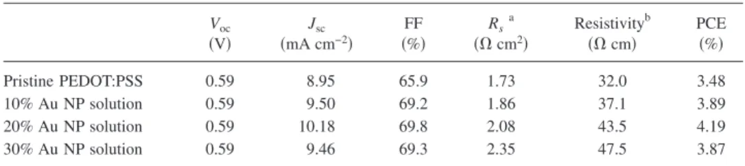
Figure1共a兲displays the J-V characteristics, recorded un-der 100 mW cm−2illumination共AM 1.5G兲, of the OPV de-vices prepared with buffer layers incorporating various amounts of Au NPs. The reference device prepared with pris-tine PEDOT:PSS exhibited an open-circuit voltage 共Voc兲 of 0.59 V, a short-circuit current 共Jsc兲 of 8.95 mA cm−2, and a fill factor 共FF兲 of 65.9%. The calculated PCE was 3.48%. After the addition of Au NPs to the buffer layer, the values of
Vocremained unchanged共0.59 V兲 but the FFs improved con-siderably 共Table I兲. We also observed a noticeably upward
trend in the values of Jscafter introducing the Au NPs. For
the devices prepared with PEDOT:PSS blended with 10% and 20% Au NP solutions, these values were 9.50 and 10.18 mA cm−2, respectively, with the PCEs increasing to 3.89% and 4.19%, respectively. On the other hand, a further increase in the concentration of the Au NP solution to 30% led to a decrease in the value of Jsc, presumably due to en-hanced backward scattering and/or increased resistivity of the buffer layer. From the result of the four-point probe mea-surement, we found that the resistivity of the buffer layers increased after embedding the Au NPs 共TableI兲. We suspect
that this behavior arose from a possible change in the mor-phology of the PEDOT:PSS blend. Accordingly, the values of the device series resistance共Rs兲 extracted from the inverse slopes of the dark J-V curves at a voltage of 1.5 V also increased after incorporating the Au NPs共TableI兲, revealing
that the enhanced performance of the OPV devices did not result from a reduction in device resistance. Table I summa-rizes the device characteristics.
Figure1共b兲displays the incident photon-to-electron con-version efficiency共IPCE兲 curves of our various devices. The trends in the IPCE follow those for the values of Jsc. Within the wavelength range from 400 to 600 nm, the photocurrent increased notably after incorporating the Au NPs. The wave-length range of spectral response enhancement coincides with the excitation range of Au NPs 共Fig.2兲, indicating that
excitation of the LSPR indeed improved the photocurrent. Note that the absorption peak of the Au NP solution was located at approximately 530 nm, whereas that of the Au NPs embedded in the PEDOT:PSS blend was located at approxi-mately 490 nm共Fig.2兲. This phenomenon is associated with
the resonance peak of NPs depending strongly on their sur-rounding media.13,14,16
To further investigate the underlying mechanism respon-sible for the enhanced performance of the devices, we com-pared the maximum exciton generation rates共Gmax兲 and ex-citon dissociation probabilities for devices prepared using pristine PEDOT:PSS and PEDOT:PSS doped with 20% Au NP solution, following the analytical approach reported by Mihailetchi and co-workers.19,20 Figure 3 reveals the effect of the LSPR on the photocurrent density 共Jph兲. We deter-mined the value of Jphusing the equation Jph= JL− JD, where
JLand JDare the current densities under illumination and in the dark, respectively. The plot of Jph with respect to the effective voltage 共Veff= Vo− Va兲, where Vo is the voltage when Jph equals zero 共i.e., JL= JD兲 and Va is the applied voltage, reveals two distinct regimes; one where the value of
Jph increased linearly with increasing voltage at a low value of Veff and another where it reached a saturated level at a sufficiently high value of Veff. The saturation photocurrent
FIG. 2. 共Color online兲 Absorption spectra of Au NPs embedded in the PEDOT:PSS matrix共solid line兲 and in solution 共dashed line兲. Inset: SEM image of the PEDOT:PSS film prepared with 20% Au NP solution blended into the matrix. A neat PEDOT:PSS film was used as the baseline for mea-surement of the absorption of the PEDOT:PSS composite films.
TABLE I. Photovoltaic characteristics of OPVs incorporating PEDOT:PSS doped with various concentrations of Au NP solutions. Voc 共V兲 Jsc 共mA cm−2兲 FF 共%兲 Rs a 共⍀ cm2兲 Resistivityb 共⍀ cm兲 PCE 共%兲 Pristine PEDOT:PSS 0.59 8.95 65.9 1.73 32.0 3.48 10% Au NP solution 0.59 9.50 69.2 1.86 37.1 3.89 20% Au NP solution 0.59 10.18 69.8 2.08 43.5 4.19 30% Au NP solution 0.59 9.46 69.3 2.35 47.5 3.87
aDevice series resistance共R
s兲 of the OPV obtained from the inverse slope of the dark J-V curve at a voltage of
1.5 V.
bResistivity of the buffer layer determined using the four-point probe method.
013305-2 Chen et al. Appl. Phys. Lett. 95, 013305共2009兲
This article is copyrighted as indicated in the article. Reuse of AIP content is subject to the terms at: http://scitation.aip.org/termsconditions. Downloaded to IP: 140.113.38.11 On: Wed, 30 Apr 2014 14:59:02
density共Jsat兲, which is independent of the bias and tempera-ture, correlates with the value of Gmax, given by Jsat = qGmaxL, where q is the electronic charge and L is the thick-ness of the active layer共L=180 nm兲. As a result, the values of Jsatfor the devices prepared with pristine PEDOT:PSS and PEDOT:PSS doped with 20% Au NP solution were 110 and 119 A m−2, respectively, and the calculated values of Gmax were 3.82⫻1027 and 4.13⫻1027 m−3s−1, respectively. Be-cause the value of Gmaxis governed only by the absorption of light,19,20the enhanced value suggests that the incorporation of the Au NPs increased the degree of light harvesting in the devices.
The exciton dissociation probability can be obtained from the normalized photocurrent density 共Jph/Jsat兲.19,21 Af-ter incorporating 20% Au NP solution in the PEDOT:PSS blend, the exciton dissociation probability under the short-circuit condition共Va= 0 V兲 increased from 78.7% to 84.9%, indicating that excitation of the LSPR facilitated the excitons to dissociate into free carriers. In general, an increase in the exciton dissociation probability reduces the recombination rate and, therefore, improves the FFs of OPVs.22,23 Conse-quently, we primarily attribute the increased FF observed in Fig.1to the increased exciton dissociation probability result-ing from the local enhancement in the electromagnetic field originating from excitation of the LSPR.
In summary, we have improved the device performance of OPVs after blending Au NPs into the PEDOT:PSS layer. The unique optical properties of the LSPR, induced by the Au NPs, led to a noticeable enhancement in the photocurrent. From the observed increase in the FF, we deduced that exci-tation of the LSPR increased not only the rate of exciton
generation but also the probability of exciton dissociation. Finally, we note that this approach is quite simple and may be suitable for application to the low-temperature processes used to form flexible OPVs on plastic substrates.
This study was supported by the National Science Coun-cil, Taiwan, and the ATU plan of the Ministry of Education, Taiwan, under Grant Nos. NSC 96-2628-E-009-022-MY2 and 98-ET-E-009-005-ET.
1C. J. Brabec, N. S. Sariciftci, and J. C. Hummelen,Adv. Funct. Mater.11,
15共2001兲.
2G. Li, V. Shrotriya, J. S. Huang, Y. Yao, T. Moriarty, K. Emery, and Y.
Yang,Nature Mater. 4, 864共2005兲.
3N. S. Sariciftci, L. Smilowitz, A. J. Heeger, and F. Wudl,Science 258,
1474共1992兲.
4G. Yu, J. Gao, J. C. Hummelen, F. Wudl, and A. J. Heeger,Science 270,
1789共1995兲.
5C. J. Ko, Y. K. Lin, F. C. Chen, and C. W. Chu,Appl. Phys. Lett. 90,
063509共2007兲.
6W. L. Ma, C. Y. Yang, X. Gong, K. Lee, and A. J. Heeger,Adv. Funct.
Mater. 15, 1617共2005兲.
7M. Reyes-Reyes, K. Kim, and D. L. Carroll,Appl. Phys. Lett. 87, 083506
共2005兲.
8V. Shrotriya, E. H. E. Wu, G. Li, Y. Yao, and Y. Yang,Appl. Phys. Lett. 88, 064104共2006兲.
9A. Yakimov and S. R. Forrest,Appl. Phys. Lett. 80, 1667共2002兲. 10S. S. Kim, S. I. Na, J. Jo, D. Y. Kim, and Y. C. Nah,Appl. Phys. Lett. 93,
073307共2008兲.
11J. H. Lee, J. H. Park, J. S. Kim, D. Y. Lee, and K. Cho,Org. Electron. 10,
416共2009兲.
12A. J. Morfa, K. L. Rowlen, T. H. Reilly, M. J. Romero, and J. van de
Lagemaat,Appl. Phys. Lett. 92, 013504共2008兲.
13E. Hutter and J. H. Fendler, Adv. Mater. 共Weinheim, Ger.兲 16, 1685
共2004兲.
14K. L. Kelly, E. Coronado, L. L. Zhao, and G. C. Schatz,J. Phys. Chem. B 107, 668共2003兲.
15S. Lal, S. Link, and N. J. Halas,Nat. Photonics 1, 641共2007兲. 16M. Pelton, J. Aizpurua, and G. Bryant, Laser Photonics Rev. 2, 136
共2008兲.
17C. C. Chang, H. L. Wu, C. H. Kuo, and M. H. Huang,Chem. Mater. 20,
7570共2008兲.
18V. Shrotriya, G. Li, Y. Yao, T. Moriarty, K. Emery, and Y. Yang, Adv.
Funct. Mater. 16, 2016共2006兲.
19V. D. Mihailetchi, L. J. A. Koster, J. C. Hummelen, and P. W. M. Blom,
Phys. Rev. Lett. 93, 216601共2004兲.
20V. D. Mihailetchi, H. X. Xie, B. de Boer, L. J. A. Koster, and P. W. M.
Blom,Adv. Funct. Mater. 16, 699共2006兲.
21V. Shrotriya, Y. Yao, G. Li, and Y. Yang,Appl. Phys. Lett. 89, 063505
共2006兲.
22L. J. A. Koster, V. D. Mihailetchi, and P. W. M. Blom,Appl. Phys. Lett. 88, 052104共2006兲.
23M. M. Mandoc, W. Veurman, L. J. A. Koster, B. de Boer, and P. W. M.
Blom,Adv. Funct. Mater. 17, 2167共2007兲.
FIG. 3.共Color online兲 Plots of photocurrent density 共Jph兲 with respect to the
effective bias 共Veff兲 for devices incorporating pristine PEDOT:PSS and
PEDOT:PSS containing 20% Au NP solution.
013305-3 Chen et al. Appl. Phys. Lett. 95, 013305共2009兲
This article is copyrighted as indicated in the article. Reuse of AIP content is subject to the terms at: http://scitation.aip.org/termsconditions. Downloaded to IP: 140.113.38.11 On: Wed, 30 Apr 2014 14:59:02