A Novel Precise Step-Shaped Soft-Start Technique
for Integrated DC-DC Converter
Chun-Yu Hsieh, Yung-Chun Chuang, and Ke-Horng Chen
Electrical and Control Engineering National Chiao Tung University, Hsinchu, Taiwan
Email: [email protected]
Abstract—The advantages of this novel precise step-shaped
soft-start technique for integrated dc-dc converter are not only owning excellent constant peak current limiting capacity for any load conditions to diminish initial inrush current powerfully but also solving the over-voltage or drop-voltage problem during the changing between the start-up mode and normal operation. Furthermore, the on-chip design for this technology reduces the numbers of the external I/O pin to decrease the cost of the converter. Therefore, this novel soft-start technique is more available and smoother for integrated dc-dc converter than the conventional soft-start technique.
I. INTRODUCTION
In recent year, the power management is in a great demand for electric devices, such as TFT-LCD display systems, digital camera, cellular phone and personal digital assistance (PDA). Moreover, the dc-dc converter characterizing driving heavy load ability is one kind of the power management to supply the regulated voltages to electric systems.
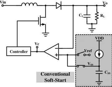
Preventing initial inrush current from causing damage to systems is an important issue for dc-dc converter. Accordingly, dual mode dc-dc converters have been developed in an effort to improve performance characteristics during start-up mode and normal operation [1] [2]. Conventionally, we use one capacitor to generate the gently ramp signal for dc-dc converter to implement soft-start during start-up as shown in Fig.1. Though the conventional soft-start reduces the damage resulted from inrush current, over-voltage or drop-voltage situation may still occur [1] [2]. For example, the voltage spikes will occur when the domination of the converter is changing between the start-up mode and the normal operation. In addition, we will consume one external pin for soft-start capacitor because this capacitor is too large to be on chip.
Because the smoother start-up is needed for dc-dc step-up converter [3] [4], the novel precise step-shaped soft-start technique is proposed. The advantages of this proposed technique are not only owning excellent peak current limiting capacity for any load conditions to diminish initial inrush current powerfully but also solving the over-voltage or drop-voltage problem. Moreover, this method also uses the on-chip technique to reduce the I/O pins for the converter [3] [4]. It is why this novel precise step-shaped soft-start technique is valuable for dc-dc converter.
The proposed soft-start technique is based on the current-mode step-up converter. For the sake of implementing this monolithic current-mode step-up converter [5]-[7], the designed is based on 0.35-µm CMOS technology. The converter is carried out by the asynchronous rectifier using Schokkty diode. The power switch, current-sensing circuit [9],
feedback control circuit, and soft-start circuit are designed on-chip. The off-chip devices of the converter are one inductor and capacitor for output stage, one capacitor and resistor for compensation.
This paper is organized as follows. The design theorem and the proposed soft-start architecture for the step-up converter are proposed in section Ⅱ . Based on this proposed architecture, the circuit implementations are presented in section Ⅲ . Simulation results are offered in section Ⅳ . Finally, the conclusions are given in section Ⅴ.
Controller Vo Vin Vref VDD VSS CSS CL RL Vc
Conventional
Soft-Start
Fig. 1. Conventional soft-start for dc-dc converter
II. DESIGNTHEOREMANDCOMPENSATIONOF
PROPOSEDARCHITECTURE
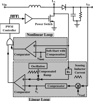
The proposed soft-start technique uses the dual loops control to implement the start-up mode and normal operation of the dc-dc step-up converter as shown in Fig.2. The nonlinear loop dominates the converter during start-up and the linear loop controls the converter during normal operation. Therefore, the proposed method is distinct from the traditional soft-start technique which only has linear loop control.
The control signal Vc in linear loop is pulled high during start-up mode. It makes the output of the comparator in the linear loop be in the logic 0. Therefore, the linear loop can’t control the power switch of the converter. Consequently, the only controller is the nonlinear loop during start-up. Moreover, the inductor current increases to make the node Lx ramp up during turning on the power switch. If the node Lx was over the voltage-limit level as shown in the node Vlimit, the output
of the comparator in the nonlinear loop becomes logic high to turn off the power switch and decreases the inductor current. As a result, the control of the nonlinear loop insures that the inductor current will limit below the specific current level determining by soft-start circuit as shown in Fig.2. Furthermore, the precise step-shaped inductor current is generated by step-up limiting levels in the different periods.
The design theorem for proposed soft-start technique are described in Section Ⅱ-A. In order to solve the oscillation and attain constant limiting capacity during nonlinear loop control, the compensation is discussed in Section Ⅱ-B.
Linear Loop Rs PWM Controller Oscillation Compensator Vo Vin Vref Sensing Inductor Current Compensated Ramp Comparator Nonlinear Loop Soft-Start with Compensation Comparator LX vlimit vc Power Switch
Fig. 2. The proposed soft-start architecture in the current-mode step-up converter
A. Design Theorem
Finding the relationship between the limiting inductor current and the output voltage is an important issue to determine what the current-limit level is set. For the dc-dc step-up converter, the relation between the inductor current and output voltage is given by
in L o dc V R V I ⋅ ⋅ =
η
2 (1) − × = o in sw in ripple V V f L V I 1 (2) ripple dc mit liI
I
I
=
+
0
.
5
(3) where Idc is the inductor current in the dc level and Irippleis the inductor current ripple. Ilimit is the limit of the inductor, RL is output load and fsw is switching frequency.According to above equations, the relation between the desired output voltage and the inductor current limiting level is given by
0
2
2
2 3=
−
−
−
Lf
V
R
V
Lf
V
I
V
R
V
L in o sw in mit li in L oη
η
(4)The equation (4) is the central rule to design the proposed architecture. At first, the max limiting level of the inductor current is set according to maximum load condition. The current-limit levels are increased through the soft-start period from zero up to the full current-limit value in five current steps for implementing the smooth start-up [3]. Furthermore, because the output voltage will be determined by this design rule, the over-voltage or drop-voltage problems will be solved during start-up. In addition, finding the on-resistance of the power switch corresponding to different output voltages is the access to set the Vlimit for getting the desired current-limit level,
Ilimit.
B. Compensation
Because the nonlinear control loop in start-up mode has the current limit capacity as like the linear loop control in normal operation, the sub-harmonic oscillation will occur during the duty is larger than 0.5 [5]-[10]. It is the reason that the compensation is necessary for the nonlinear loop to avoid the sub-harmonic oscillation as shown in Fig.3. Moreover, the slop of the compensation ramp ma must be larger than half of the descending slop of inductor current m2. Therefore, unlike the linear loop creates compensated ramp to add with sensing inductor current, the nonlinear loop control compensates the
Vlimit directly. In order to achieve the ramp down Vlimit signal, the compensation resistance and capacitor is needed to generate the ramp down compensated limiting voltage.
Another purpose for compensation is to generate the constant current limiting level with different load conditions. From equation (4), variable load conditions will cause different output voltage. However, the higher output voltages cause the smaller the on-resistances of power switch because the turn-on voltage of the power switch is provided by output voltage [6]. It is the reason that the ramp down Vlimit signal is able to ensure the current limiting level equally with any load conditions.
Initial limiting level
Inductor current
Compensated
limiting level
-m2
-ma
Fig. 3. The compensated current limiting level
III. CIRCUITIMPLEMENTATIONS
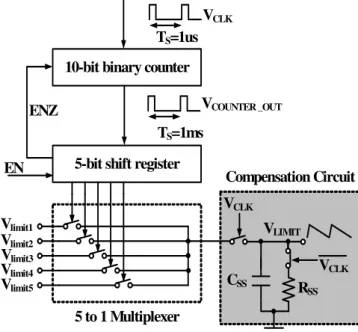
The circuits for the proposed soft-start architecture are shown in Fig.4. The one-shot clock signal, Vclk, is generated from the oscillation of the converter as shown in Fig.2. When the supply voltage of the converter reach the typical working level, the EN signal is set to be logic high to enable the system and the 5-bit shift register will turn on the first switch connecting between Vlimit1and Vlimit. The ENZ signal enables the 10-bit binary counter to create the VCOUNTER_OUT signal to trigger the 5-bit register. The shift register will turn on five switches sequentially for providing the five different limiting voltages to achieve five limit-current steps during start-up. The interval between different switching turn-on is set as 1ms to insure the raising between two specific output voltages. The maximum load current is available after the timer expires or after the output voltage reaches regulation.
The compensation circuit comprises one capacitor and one resistance. The limiting voltage utilizes the discharging of the capacitor to generate ramp down limiting signal for compensation and constant current limiting capacity. Because the compensated limiting voltage, the proposed soft-start technique not only limits the peak inductor current precisely for any load conditions but also solve the sub-harmonic oscillation problem.
5-bit shift register 10-bit binary counter
TS=1us TS=1ms Vlimit1 Vlimit2 Vlimit3 Vlimit4 Vlimit5 5 to 1 Multiplexer VCOUNTER _OUT VCLK VCLK VCLK CSS R SS VLIMIT Compensation Circuit EN ENZ
Fig. 4. The proposed soft-start circuit
IV. SIMULATIONRESULT
The HSPICE simulation results are presented in this section with 0.35µm CMOS process. The desired output voltage is 13V and the typical supply voltage is 5V. This converter is designed with L=4.7 µH and Co=22 µF at this switching
frequency of 1MHz. The off-chip compensation capacitor and resistance for dc-dc converter is 250pF and 650kΩ. However, the value of the system compensation capacitor and resistance can be modified according to the demand of the specifications
of the system. Moreover, the on-chip soft-start capacitor and resistance is 2pF and 400kΩ. The area of the soft-start circuit is suitable to design on the chip. Furthermore, the maximum load condition in this converter is 400mA. The driving load capacity for this specification is large enough to operate at the heavy load condition. The below discuss is based on the maximum load condition to start up this converter.
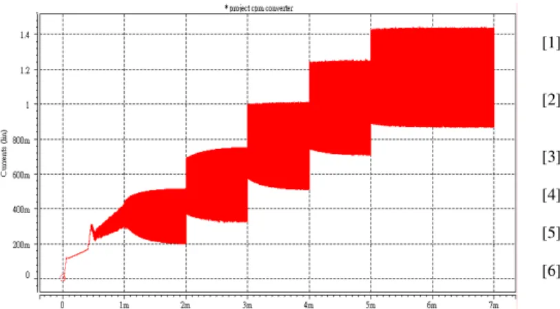
The maximum inductor is 1450mA for this load condition. As a result, setting five step-up current limiting levels, such as 500mA, 750mA, 1000mA, 1250mA, and 1450mA, achieves the precise step-shaped soft-start technique to make the inductor current ramp up step by step. The maximum current-limit level will exist continuously even if the converter is in the linear loop control. From equation (4), the output voltage corresponding to those five current limiting levels are 7.27V, 9V, 10.6V, 12V and 13V. Accordingly, the on-resistance of the power stage can be defined to determine the limiting voltage level, such as 0.2V, 0.27V, 0.34V, 0.4V and 0.45V. Moreover, the peak voltages of those limiting levels will be modified to become 0.23V, 0.31V, 0.45V, 0.57V and 0.66V for compensation. The compensation limiting voltage compares with the voltage in the node Lx as presented in Fig.5. The red line is presented for the voltage in the node Lxand the purple line is mean for Vlimit when current-limit level is 1250mA. The intersection point is 0.4V and the peak voltage of the Vlimitis 0.57V as shown in Fig.5.
The waveform of the precise step-shaped inductor current is shown in Fig.6. The supply voltage reaches the typical voltage at the 1ms and the soft-start begins to work. The five limit-current steps are obvious presented in Fig.6. Moreover, the designed converter turns on power stage by the one-shot clock during the supply voltage below the typical voltage. The time for one step is 1ms and there are five precise current limiting steps 500mA, 750mA, 1000mA, 1250mA, and 1450mA, as shown in Fig.6. The waveform of the output voltage is displayed in Fig.7. There are five voltages levels, such as 7.27V, 9V, 10.6V, 12V and 13V during different periods. The end of the soft-start operation is that the output reaches the desired output voltage. Furthermore, the advantage is replaced with the linear loop control without any voltage spikes.
Fig. 5. The waveform of the limiting voltage level and the node LX as
mentioned in proposed architecture.
Fig. 6. The waveform of the inductor current of the step-up converter
Fig. 7. The waveform of the output voltage of the step-up converter .
V. CONCLUSION
The novel step-shaped soft-start technique for the dc-dc converter not only has excellent constant peak current limiting capacity for any load conditions to diminish initial inrush current efficiently but also solves the over-voltage or drop-voltage problem during start-up. Furthermore, the on-chip design from this technology reduces the numbers of the external I/O pin to decrease the cost of the converter. The comparison between the conventional soft-start and proposed soft-start is shown in TABLE 1. In a word, this novel structure provides the powerful peak current limiting ability to prevent the electric systems from affecting inrush current damage and is available for dc-dc converter.
TABLE1
THE COMPARISONOF DIFFERENT SOFT-START ARCHITECTURE The comparison of the soft-start architecture Conventional structure Proposed structure
Current limiting ability
Depending on load Constant
Voltage
spikes Usually happening Never happening
The cost for chip
Needing external capacitor On-chip design
REFERENCES
[1] Marcus Marchesi Martins, “SOFT-START SYSTEM FOR VOLTAGE REGULATOR AND THE METHOD OF IMPLEMENTING SOFT-START,” U.S. patent 0027106, Texas Instruments Inc, 2004. [2] Hirokazu Tsujimoto and Tetsuo Tateishi, “SOFT STARTING
REFERENCE VOLTAGE CIRCUIT,’ U.S. patent 6348833, Kabushiki Kaisha Toyoda Jidoshokki Seisakusho, 2002.
[3] “MAX1518:TFT-LCD DC-DC Converter with Operational Amplifier,” MAXIM Integrated Products Inc, 2004.
[4] “MAX1748;MAX8726: Triple-Output TFT-LCD DC-DC Converters,” MAXIM Integrated Products Inc, 2004.
[5] Robert W. Erickson, Dragan Maksimović, Fundamentals of Power
Electronics, 2nd ed., KLUWER ACADEMIC PUBLISHERS, 2001. [6] Cheung Fai Lee and Philip K.T.Mok, ”A Monolithic Current-Mode
CMOS Converter With On-Chip Current-Sensing Technique,” IEEE
JOURNAL OF SOLID-STATE CIRCUITS, VOL.39, NO.1, JANUARY 2004.
[7] Chi Vat Leung, Philip K.T. Mok, “A 1-V Integrated Current-Mode Boost Converter in Standard 3.3/5-V CMOS Technologies,” IEEE
JOURNAL OF SOLID-STATE CIRCUITS, VOL.40, NO.11, NOVERMBER 2005.
[8] Haifei Deng, Xiaoming Duan, Nick Sun, Yan Ma, Alex Q.Huang and Dan Chen,” Monolithically Integrated Boost Converter Based on 0.5-µm CMOS Process,” IEEE TRANSACTIONS ON POWER
ELECTRONICS. VOL.20, NO.3, MAY 2005
[9] Hylas Y.H Lam, Wing-Hung Ki and Dongsheng Ma, “LOOP GAIN ANALYS AND DEVELOPMENT OF HIGH-SPEED HIGH ACCURACY CURRENT SENSORS FOR SWITCHING CONVERTERS,” ISCAS 2004
[10] Mossoba, J.T., Krein, P.T., “Small signal modeling of sensorless current mode controlled DC-DC converters”. Computers in Power
Electronics, 2002. Proceedings. 2002 IEEE Workshop on, pp. 23-28, June 2002