A Low Phase-Noise Voltage-Controlled SAW
Oscillator With Surface Transverse Wave
Resonator for SONET Application
Jon-Hong Lin, Student Member, IEEE, and Yao-Huang Kao, Member, IEEE
Abstract—A surface transverse wave (STW) resonator-based
oscillator was developed in response to SONET OC-48 application. To meet the low jitter objective, a high- STW resonator was designed and fabricated in this study. The residual phase-noise measurement techniques are used to evaluate the feedback os-cillator components, such as the loop amplifier, STW resonator, and electronic phase shifter, which can play important roles in determining the oscillator’s output phase-noise spectrum. The os-cillator’s white phase-noise floor is 170 dBc/Hz for carrier-offset frequency greater than 1 MHz. The oscillator’s phase-noise level is 67 dBc/Hz at a 100-Hz carrier offset. Both low close-in phase-noise and low white phase-noise floor makes the oscillator meet low jitter requirement. The electronic frequency tuning range exceeds 200 ppm. The oscillator provides 13.5 dBm of output power and consumes 65 mA from+5–V power supply.
Index Terms—Phase noise, SONET, surface acoustic wave
(SAW), voltage-controlled oscillators (VCOs).
I. INTRODUCTION
I
N HIGH-SPEED digital communication systems, a clock recovery circuit is used for data integrity. The clock is usually extracted from a phase-locked-loop circuit with a low jitter voltage-controlled oscillator (VCO). Due to the avail-ability of high frequency and high-quality (high- ) resonator, the VCOs were mostly fabricated at 622 MHz either by the fourth harmonic of 155-MHz crystal oscillator (VCXO) or directly by the 622-MHz voltage-controlled saw oscillator (VCSO) [1], [2]. Both cases suffer from the degradation factor of dB on the phase noise as applications to OC-48 at 2488.32 MHz. Seldom studies on 2488 MHz have been presented [3]–[5]. In this study, a highly stable VCSO with a surface transverse wave (STW) resonator working directly at 2488.32 MHz is developed. The high- STW resonator on quartz was demonstrated in 1987 [6]. Its advantages over the conventional Rayleigh waves are the very high velocity and low propagation loss [7]. The wave velocity of the STW is approximately 5000 m/s. High wave velocity makes the Manuscript received December 29, 2005; revised September 10, 2006. This work was supported by the ftech Company and by the Southern Taiwan Science Park Administration under Contract 92-1001-B062-001.J.-H. Lin is with the Institute of Communication Engineering, Na-tional Chiao-Tung University Hsin-Chu, Taiwan 30050, R.O.C. (e-mail: nick.cm88g@nctu.edu.tw).
Y.-H. Kao is with the Department of Communication Engineering, Chung-Hua University, Hsin-Chu, Taiwan 300, R.O.C. (e-mail: yhkao@chu. edu.tw).
Digital Object Identifier 10.1109/TMTT.2006.888575
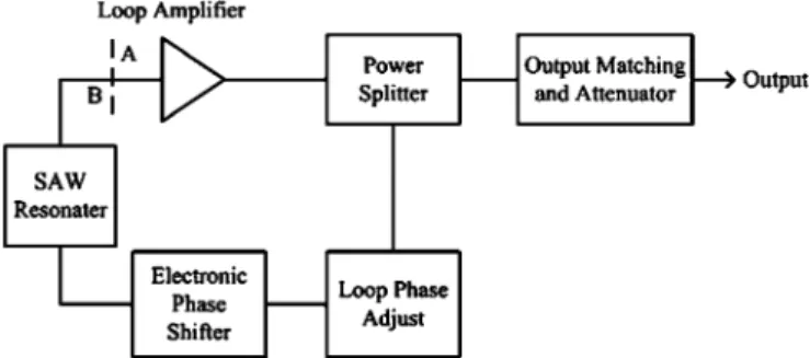
Fig. 1. Block diagram of a feedback loop oscillator.
inter-digit transducer (IDT) wider and then slightly reduces the requirement of the photolithography process. A coupled-mode resonator is carefully designed to accommodate the request of wide band tuning and low phase-noise applications. The unloaded quality factor equal to 5500 was realized in this study. It is essential to choose the proper elements to achieve low phase noise. Here, the residual phase noise in each module is carefully evaluated. Residual noise is the noise added to a signal when the signal is processed by a two-port device and it is composed of both AM and FM components. The residual phase-noise measurement techniques [8] are employed to eval-uate the components of the feedback loop oscillator, such as the loop amplifier, STW resonator, and electronic phase shifter, which can play important roles in determining the oscillator’s output phase-noise spectrum. Agilent’s E5503B phase-noise measurement system was used to measure the residual phase noise of each component and the phase noise of the VCSO. The phase noise of this oscillator is approximately 67 dBc/Hz at 100-Hz offset. The measured white phase-noise floor of the oscillator is 170 dBc/Hz. Both low close-in phase-noise and low white phase-noise floor makes the oscillator meet low jitter requirement. The electronic frequency tuning range exceeds 200 ppm. The oscillator provides 13.5 dBm of output power and consumes 65 mA from 5-V power supply. High output power makes the oscillator be able to drive emitter-coupled logic (ECL) circuits directly without using an extra buffer amplifier.
II. OSCILLATORDESIGN
It is noted that the oscillator with a one-port surface acoustic wave (SAW) resonator suffers from large parasitic capacitance from IDTs. Here, the architecture with a two-port resonator forming a feedback loop is chosen as shown in Fig. 1.
It consists of a single-loop amplifier, an electronic phase shifter, a lumped-element reactive Wilkinson power splitter, a lumped-element reactive phase adjusting, and a two-port STW resonator. The resonator acts as a short circuit with zero phase shift at the desired frequency. No output buffer amplifier is used because it may degrade the oscillator’s white phase-noise floor. The oscillation starts as the closed-loop gain satisfies Barkausen’s criteria.
During design phase, the open-loop gain is evaluated by breaking the loop at the appropriate plane with equal input and output impedances, as noted by line AB in Fig. 1. Here, the impedances are 50 , seen from network analyzer mea-surement. The impedance of each module is actually set to 50 for convenience. This approach has the advantage that the noise characteristics of the individual component as measured in an open-loop configuration have a direct bearing on the closed-loop phase noise of the oscillator.
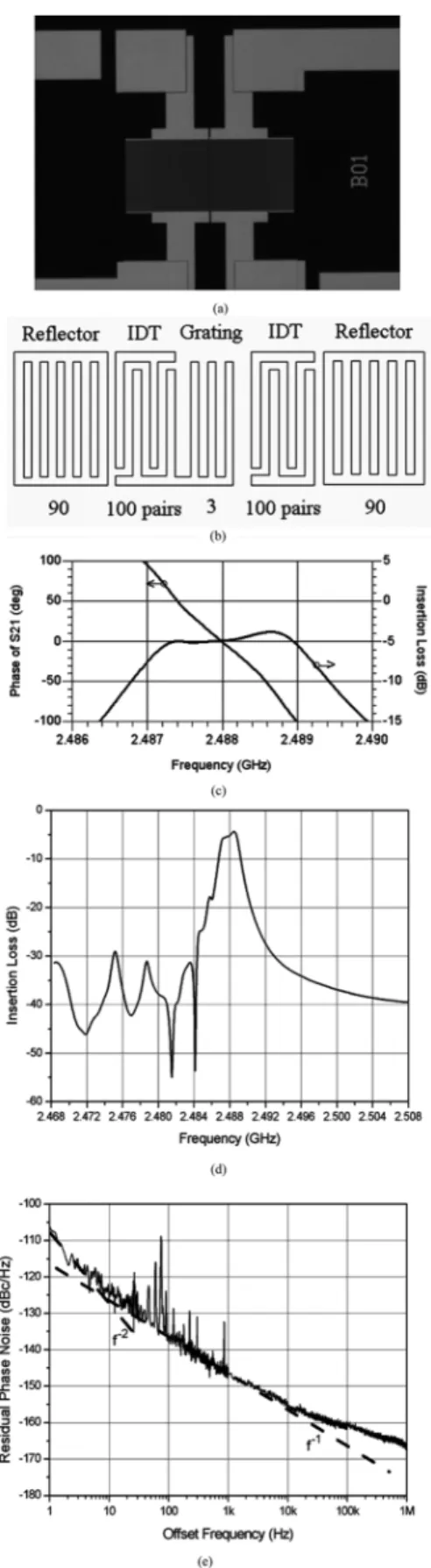
To achieve low insertion loss, high frequency, and high-factor, the SAW resonator with STW is employed. The STW is a shear wave with very high velocity and energy trapping. It can reduce the diffraction of the shallow bulk wave into the substrate and lead to the decrease in device insertion loss and in-crease in the resonator . The width of the transducer is approx-imately 0.5 m. The overlap aperture is approxapprox-imately 250 m. This larger transducer width also makes it possible to mass pro-duce the resonator with acceptable yield. Since the STW does not associate volume charge with propagation, its propagation loss is small [7] To achieve the proper turnover temperature, the ST-cut quartz 90 , Euler angles (0 , 132, 75 , 90 ), is employed as the substrate of this resonator, which has the turnover temper-ature approximately at 45 C. This fetemper-ature makes the oscillator without extra temperature compensation circuit work well in the real environment. It simplifies circuit design and lowers the cost. The resonator is detailed in Fig. 2(a) and (b). The die size is 1.8 mm 1.2 mm. Two shorted reflectors (90 fingers) are placed outside the input and output IDTs (100 pairs). A shorted grating with three fingers is placed between the input and output IDTs. The resonant modes formed by input and output IDTs are cou-pled just as two coucou-pled parallel LC resonators. The coupling is carefully tuned by the central grating. This results in a two-mode response such as that shown in Fig. 2(c). Due to the grounding grating, the insertion loss is reduced to 4–5 dB, which is much smaller than that of 10–15 dB in a conventional SAW or STW delay line. [5] The approximate linear phase change obtained within the 3-dB bandwidth equals to 1.713 10 rad/Hz. The upper and lower limits of the phase change are above 90 . The
estimated loaded factor is equal to 1537.
The group delay is approximately 1.713 10 rad/Hz. High insertion loss out of the passband is revealed in Fig. 2(d). The spurious out of passband is suppressed under 30 dB. The center frequency is trimmed to 2488.32 MHz. The residual phase noise is as shown in Fig. 2(e). It is measured by applying the drive power approximately the same as the power in the steady-state oscillation condition. The corner of the flicker noise is out of the scope of this measurement.
The HBT monolithic amplifier is selected as the loop ampli-fier because of low noise figure and high dynamic range. The dB is at 17 dBm and the bandwidth is 4 GHz. Its bandwidth
Fig. 2. (a) Photograph and (b) block diagram of the STW resonator. (c) Phase and insertion loss responses from 2.486 to 2.490 GHz. (d) Insertion loss from 2.468 to 2.508 GHz. (e) Residual phase noise of STW resonator.
was properly selected to prevent high second harmonics. The nominal gain of 17 dB is much greater than that required to over-come the total loop losses to insure the stable oscillation. The magnitude of gain variation over temperature is approximately
Fig. 3. Residual phase noise of loop amplifier.
Fig. 4. Residual phase noise of electronic phase shifter.
0.005 dB C and this feature can prevent the AM–PM noise caused by the temperature variation. The residual phase noise is shown in Fig. 3. The noise floor is approximately 170 dBc/Hz with a flicker noise corner at 17-kHz offset.
Since the white phase-noise floor will be raised by a resistive attenuator in the feedback loop, an unequal Wilkinson power splitter is employed to adjust the excess loop gain instead of a resistive attenuator [9]. To save the volume, the circuit is real-ized by the lump reactive components instead of a transmission line.
The electronic phase shifter is used to tune the oscillation fre-quency. The electronic phase shifter is constructed with induc-tors and two silicon tuning diodes using a T-circuit structure. The phase noise and tuning linearity will be affected by the tuning diodes. High residual phase noise of the tuning diodes will degrade the phase noise of the VCO. The residual phase-noise performance is shown in Fig. 4. With proper selection of varactor diodes, the high tuning linearity and low residual phase noise are achieved at the same time.
Fig. 5. Total phase shift and the open-loop gain at the oscillation frequency.
The phase shift of the loop amplifier and power splitter is approximately equal to 80 and 90 , respectively. The electronic phase shifter is approximately 40 . Since the total phase shift around the loop must be rad, another 10 is required, which is from the loop phase adjust constructed with fixed lumped reactive components. The frequency dependences of the total phase shifter and open-loop gain seen from the reference plane A-B line indicated in Fig. 1 are shown in Fig. 5.
Curves and are the total phase shift with V and V, respectively. Curves and are the re-spective open-loop gain with V and V, respectively. The group delay is approximately 1.74 10 rad/Hz. As com-pared to Fig. 2(c), we see that the SAW resonator dominates the change of the total phase shift. The slight increase in group delay may be from the tunable phase shifter with varactors. The oscillation frequency is predicted at the zero-crossing point with enough gain margins at approximately 2 dB. This gives us the benefit of low flicker noise from the amplifier without deep gain compression. The tuning bandwidth is approximately equal to the resonator’s 1-dB bandwidth. It is approximately from 2487.85 to 2488.85 MHz.
III. OSCILLATORPERFORMANCES
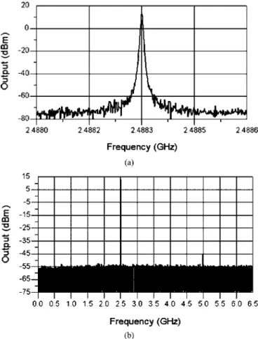
The performances of the oscillator with an STW resonator are measured. The narrow and wide scan of the output spectrum and relative levels of the harmonic are shown in Fig. 6(a) and (b), respectively. Since the STW resonator do not have a second harmonic response and the bandwidth of the loop amplifier is limited under 4 GHz, the second harmonics of the oscillator is suppressed below 58 dB, as shown in Fig. 6(b), without any output low-pass filter.
The tuning characteristic is shown in Fig. 7(a) with 200-ppm range and good linearity. The frequency depen-dence on temperature is illustrated in Fig. 7(b). The turnover temperature is approximately 45 C, which is mainly deter-mined by the STW resonator.
The frequency discriminator method was used to measure the phase noise of the VCSO [11], [12]. The delay line frequency discriminator is implemented with Agilent’s E5503B phase noise measurement system and a delay line. Unlike the phase detector method, the frequency discriminator method does not require a second reference source phase locked to the de-vice-under-test (DUT). This makes the frequency discriminator method extremely useful for measuring sources that are difficult
Fig. 6. (a) Measured output spectrum for the 2488.32-MHz and (b) harmonic spectrum.
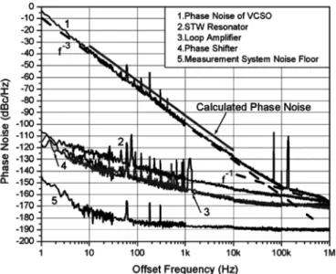
to phase lock, especially for the free-running VCOs that are drift quickly. The delay line frequency discriminator converts short-term frequency fluctuations of the source into voltage fluctuations that can be measured by a baseband analyzer. The conversion is a two-part process, first converting the frequency fluctuations into phase fluctuations, and then converting the phase fluctuations into voltage fluctuations. The output power of the DUT is divided between a delay line and the local oscillator input of a double-balanced mixer. The frequency fluctuations to phase fluctuations transformation takes place in the delay line. As the frequency changes slightly, the phase shift incurred in the fixed delay time will change proportionally. The delay line converts the frequency change at the line input into the phase change at the line output when compared to the undelayed signal arriving at the mixer in the second path. The double-balanced mixer, acting as a phase detector, transforms the instantaneous phase fluctuations into voltage fluctuations. With the two signals 90 out of phase, the IF voltage output of the mixer is proportional to the input phase fluctuations. The voltage fluctuations can then be measured by the baseband an-alyzer and converted to phase-noise units. A 312-ns delay line implemented by an ANDREW LDF5–50A low-loss coaxial cable was used in the measurement. Long enough delay time is needed to ensure the sensitivity of measurement system. The phase noise of the oscillator is measured as shown in Fig. 8. The measured parameters of this VCSO and the specifications of the other commercial products are summarized in Table I.
Fig. 7. Dependence of the oscillation frequency on: (a) tuning voltage and (b) temperature.
The spectral shape in curve 1 indeed arrears near the carrier. The intersection point with the curve is around 50-kHz offset. The phase noise is 153 dBc/Hz at 100-kHz offset, which is lower than those indicated in Table I.
To analyze the shaping behavior of the close loop, the residual phase noises are examined. For comparison, the residual phase noises in components are also presented in Fig. 8. It reveals that the noise from the STW resonator (curve 2) is dominant at approximately 10 dB above those from the amplifier (curve 3) and phase shifter (curve 4). The phase shifter has the same order of magnitude as that in the loop amplifier. The system’s floor is also indicated as shown by curve 5, which is much lower than the measured items.
As referred to Fig. 5, the magnitude of the loop gain under steady state is assumed to one with a rather wide bandwidth, at least 500 kHz at 2488.32 MHz. The phase is assumed linear with slope or group delay , which roughly equals to 1.74 10 rad/Hz in our case, within the limited bandwidth.
Fig. 8. Measured phase noise for the 2488.32-MHz STW oscillator.
TABLE I
MEASUREDRESULT FOR THEVOLTAGE-CONTROLLED
STW OSCILLATOR ANDCOMPARISONWITH THEOTHERS
Hence, the normalized open-loop gain is written as , where is the offset frequency from the center frequency. The closed-loop gain is then obtained as
Closed-loop gain
According to [9], the power spectral density (PSD) of phase noise can be shaped by multiplying the square of the closed-loop gain to the residual phase noise. Here, the shaping factor for the PSD is [10]. As near to the carrier with small , the shaping appears as . It is concluded that the phase noise is indeed shaped from the residual noise by the term, which is originated from the high- res-onator. The calculated results are in good agreement with the measurements.
IV. CONCLUSIONS
A STW-based oscillator was designed and fabricated in this study. The resonator is operated directly at the specific
frequency of 2.48 GHz to avoid the degradation of phase noise due to frequency multiplication. Two-coupled modes are designed to achieve wide tuning. Trimming the central grating while keeping the steep phase change enhances the tuning bandwidth of resonator. The tuning capability achieves 200 ppm. In comparison with the other commercial products, the phase-noise performance of this study is better than 8 dB at 100-kHz offset frequency. The white phase-noise floor is approximately 170 dBc/Hz in this study. The phase-noise near carrier is confirmed to follow the prediction of Leeson’s model. It is concluded that the behavior of phase noise is dominated by the residual noise of the SAW resonator and is shaped by the important factor of group delay.
ACKNOWLEDGMENT
The authors would like to thank Dr. L. Wu, ftech Company, Tainan, Taiwan, R.O.C., for fabricating the STW resonator and Dr. B. Temple, Agilent Technologies, Spokane, WA, for the measurement of phase noise.
REFERENCES
[1] O. Ishii, H. Iwata, M. Sugano, and T. Ohshima, “UHF AT-CUT crystal resonators operating in the fundamental mode,” in IEEE Int. Freq.
Con-trol Symp., 1998, pp. 975–980.
[2] N. Nomura, M. Itagaki, and Y. Aoyagi, “Small packaged VCSO for 10 Gbit Ethernet application,” in IEEE Int. Ultrason., Ferroelectr., Freq.
Control Symp., 2004, pp. 418–421.
[3] B. Fleischmann, A. Roth, P. Russer, and R. Weigel, “A 2.5 GHz low noise phase locked surface transverse wave VCO,” in IEEE Int.
Ul-trason., Ferroelectr., Freq. Control Symp., 1989, pp. 65–69.
[4] I. D. Avramov, “Very wide tuning range, low-noise voltage controlled oscillators using ladder type leaky surface acoustic wave filters,” in
IEEE Ultrason., Ferroelectr., Freq. Control Symp., 1998, pp. 489–496.
[5] C. E. Hay, M. E. Harrell, and R. J. Kansy, “2.4 and 2.5 GHz miniature, low-noise oscillators using surface transverse wave resonators and a SiGe sustaining amplifier,” in IEEE Ultrason., Ferroelectr., Freq.
Con-trol Symp., 2004, pp. 174–179.
[6] T. L. Bagwell and R. C. Bray, “Novel surface transverse wave res-onators with low loss and highQ,” in Proc. IEEE Ultrason. Symp., 1987, pp. 319–324.
[7] H. Ken-ya, Surface Acoustic Wave Devices in Telecommunications. Berlin, Germany: Springer-Verlag, 2000.
[8] G. K. Montress, T. E. Parker, and M. J. Loboda, “Residual phase noise measurements of VHF, UHF, and microwave components,”
IEEE Trans. Ultrason., Ferroelectr., Freq. Control, vol. 41, no. 5, pp.
664–679, Sep. 1994.
[9] T. E. Parker and G. K. Montress, “Precision surface acoustic wave (SAW) oscillator,” IEEE Trans. Ultrason., Ferroelectr., Freq. Control, vol. 35, no. 3, pp. 342–364, May 1988.
[10] D. B. Leeson, “A simple model of feedback oscillator noise spectrum,”
Proc. IEEE, vol. 54, no. 2, pp. 329–330, Feb. 1966.
[11] D. Scherer, “Design principles and measurement of low phase noise RF and microwave sources,” presented at the Hewlett-Packard RF and Microw. Meas. Symp. and Exhibition, Hasbrouck Heights, NJ, 1979. [12] C. Schiebold, “Theory and design of the delay line discriminator for
phase noise measurement,” Microw. J., pp. 103–112, Dec. 1983. [13] I. D. Avramov, O. Ikata, T. Matsuda, and Y. Satoh, “High-performance
surface transverse wave based voltage controlled feedback oscillators in the 2.0 to 2.5 GHz range,” in Proc. IEEE Int. Freq. Control Symp., 1998, pp. 519–527.
[14] J. H. Lin and Y. H. Kao, “A low phase noise voltage controlled saw oscillator with surface transverse wave resonator for SONET applica-tion,” in IEEE Int. Asia–Pacific Microw. Conf., Suzhou, China, 2005, vol. 2, pp. 973–976.
Jon-Hong Lin (S’04) was born in Tainan, Taiwan,
R.O.C., in 1970. He received the B.S. degree in electrical engineering from National Cheng-Kung University, Hsin-Chu, Taiwan, R.O.C., in 1994, the M.S. degree in communication engineering from National Chiao-Tung University, Hsin-Chu, Taiwan, R.O.C., in 2001, and is currently working toward the Ph.D. degree in communication engineering at National Chiao-Tung University.
Yao-Huang Kao (M’76) was born in Tainan,
Taiwan, R.O.C., in 1953. He received the B.S., M.S., and Ph.D. degrees in electronic engineering from National Chiao-Tung University, Hsin-Chu, Taiwan, R.O.C., in 1975, 1977, and 1986, respectively.
In 1986, he joined the Department of Communica-tion Engineering, NaCommunica-tional Chiao-Tung University. He is currently with the Department of Communica-tion Engineering, Chung-Hua University, Hsin-Chu, Taiwan, R.O.C., where he is a Professor. He has also been a Visiting Scholar involved with research in nonlinear circuits with the University of California at Berkeley (1988) and Bell Communication Research (Bellcore) (1989). He is also a Technical Consultant for RF circuits for both industry and government institutes. His current research interests involve nonlinear dynamics and chaos, high-speed optical communications, and microwave and CMOS RF circuit designs.