國
立
交
通
大
學
材料科學與工程學系
博 士 論 文
覆晶封裝銲錫接點在電遷移效應下之熱與電特性
Thermo-electrical characterizations in flip-chip
solder joints during electromigration
研究生:梁世緯
指導教授:陳智 教授
覆晶封裝銲錫接點在電遷移效應下之熱與電特性
Thermo-electrical characterizations in flip-chip solder joints during
electromigration
研 究 生: 梁世緯 Student: Shih-Wei Liang
指導教授: 陳智 Advisor: Dr. Chih Chen
國立交通大學
材料科學與工程所
博士論文
A Thesis
Submitted to Department of Materials Science and Engineering
College of Engineering
National Chiao Tung University
in partial Fulfillment of the Requirements
for the Degree of Ph.D. in Materials Science and Engineering
July 2009
Hsinchu, Taiwan, Republic of China
i
覆晶封裝銲錫接點在電遷移效應下之熱與電特性
學生:梁世緯
指導教授:陳智 博士
國立交通大學材料科學與工程學系
摘 要
覆晶封裝銲錫接點的電遷移與熱遷移是可靠度上的重要議題,是
故了解覆晶封裝銲錫接點的熱電效應相當重要。本研究利用實驗與有
限元素分析法研究銲錫接點在測試時的熱電特徵。首先利用聚焦離子
束製備出具有記號的銲錫接點,驗證出電遷移速率與電流密度呈現正
比的關係;再者因為四點量測的結構改用,可以使得凸塊電阻可直接
量測出來,並且在不同位置量測到的電阻有所不同;隨著電遷移產生
孔洞並成長,使得電流密度與溫度重新分佈的情形都可以利用模擬得
知,會發現銲錫接點內部的電流密度與溫度在孔洞生成
50%時,會先
些許下降,當孔洞持續成長的時候,電流密度與溫度會改為上升;此
外利用不同線寬的導線研究導線寬度對電遷移壽命的影響,發現導線
線寬會影響電流集中效應與焦耳熱效應,但主要還是熱的影響,使得
線寬比較寬的時候,壽命得以延長;另外還討論銲錫接點在通電後期
ii
造成的熔化,主要是來自於導線的劣化損壞,使得溫度急遽上升達到
熔點;最後,因為電流集中效應的關係,使得覆晶封裝銲錫接點內部
的溫度呈現非線性分佈。
另外利用模擬的結果討論利用變換底部金屬層材料、鋁導線設
計、底部金屬層厚度以及接觸窗口大小,設法找出覆晶封裝銲錫接點
之最佳化結構,以供後續設計之參考。最後在分析當銲錫接點越做越
小時,對溫度與電流密度之影響,並對矽晶片在三度空間堆疊下,將
會減薄矽晶片厚度,而當矽晶片變薄之下,對銲錫接點溫度之影響。
此些議題將在此研究裡詳細地討論。
iii
Thermo-electrical characterizations in flip-chip
solder joints during electromigration
Student:Shih-Wei Liang
Advisor:Dr. Chih Chen
Department of Materials Science and Engineering
National Chiao Tung University
Abstract
Electromigration and thermomigration are two important issues in
flip-chip solder joints under current stressing. Thus, to investigate the
current density and temperature distribution is quite valuable. In this
study, the experiments and finite-elements method were used to
understand the thermo-electrical characterizations in flip-chip solder
bumps under current stressing.
The observation of marker movement made by focused ion beam
(FIB) confirmed that the electromigration flux is proportional to the
current density. Using the four-point probing, the bump resistance was
measured directly. Also, the bump resistance changed due to the change
iv
of measuring position. Due to the void formation and propagation, the
current density and temperature re-distributed. Before the voids grew and
became 50% of the contact opening, the current density and temperature
decreased slightly. When the voids continuously grew, the current density
and temperature increased. The width of Al trace affected the current
crowding and Joule heating effect in the flip-chip solder joints. The main
effect on mean-time-to-failure (MTTF) is the Joule heating effect. Then,
the key reason causing the solder melting at the final stressing period is
the degradation of Al trace. Rapid increase in Al trace resistance caused
the abrupt Joule heating to melt the solder bumps. The non-linear thermal
gradient was found in flip-chip solder joints under current stressing due to
current crowding effect.
In addition, the simulation study was carried out in order to find the
suitable UBM material, Al trace’s designation, the thickness of UBM and
the size of contact opening, so as to determine the optimal structure of
flip-chip solder joints. These results are useful guidelines for later
designation. Afterward, to analyze its effects on temperature and electric
current density when the size of flip-chip solder joints shrink. When
pilling up in three dimensions, Si chip will be thinner, the effect of this
change on flip-chip solder joints will thoroughly be discussed as well.
v
Acknowledgements
感謝我的指導教授陳智老師,在我還是應數系的時候可以收我做為專題生, 之後鼓勵我攻讀材料所碩博士,老師對我的指導不僅是在專業的研究領域,做人 處事方面也是我值得學習的楷模。陳智老師給我有許多參與國際研討會的機會, 甚至讓我可以出國執行千里馬計畫一年,眾多的出國經驗不僅讓我體驗各國風 情,更重要的是培養我的國際觀,不會只是閉門造車。在 UCLA 的期間,我特 別要感謝杜經寧院士對我的照顧,杜老師把我當成自己的學生一樣,細心教導, 傳授許多平時會忽略的物理觀念,對我的研究有甚多幫助,對我的生活也是關心 有加,讓我在LA 並沒有太嚴重的思鄉情結。在此也要感謝我的口試委員:高振 宏教授、謝宗雍教授、饒達仁教授與賴逸少博士,對我論文的批評與指教,讓我 知道我的學習仍然不足,我必須更嚴謹的態度來面對我的研究。 不能忘記的還有一路上陪我的一起努力,互相砥礪的學長姐與學弟妹們:感 謝穎超學長,無時不刻對我的耳提面命,常常在人生的道路上指引我;棟樑學長 與大鈞帶領我進入到模擬的領域,讓我得以完成我的博士論文;慶榮學長與章賓 學長教導我對儀器操作與實驗進行,讓我都有莫大的啟發;給我快樂的書宏學長 與鈺庭學長,常常在實驗煩悶之餘,讓我覺得還有溫暖跟開心;謝謝聖翔學長與 翔耀在實驗上的協助,讓我可以能完善的分析;還有筱芸學姊與阿丸,更是我最 無所不聊的好友,謝謝你們的耐心,常常可以讓我發洩;忠厚老實的詠湟學長和 可愛的佳凌學妹,更是讓我永難忘懷,我會常常回來找你們;感謝阿光學長、德 聖學長、淵明學長、宏誌學長、程昶學長與佩君學姐,在我剛進實驗室對我的照 顧;一起打拼的哲誠、舜民、俊宏和健民,發現我們曾經的擁有,卻是那樣的永 恆;還有我最喜歡的學弟妹們宗寬、誠風、小山、宗憲、旻峰跟明慧,看著你們 畢業的時候,那種離情依依的感覺,自今還感動萬分;新加入實驗室的學弟妹們, 漢文、岱霖、瑋安、建志、右峻、若薇跟曉葳,祝福你們可以順利的完成之後的 實驗,快快樂樂畢業;以及我最愛的系辦小姐們:蕙馨、克瑤與麗娟,有你們的 幫忙,才讓我可以順利畢業。有你們的陪伴,實驗室的生活是如此的多采多姿與 充滿歡樂。 在UCLA 的朋友們,我的好室友居呈學長、苡嘉、欣蘋、汎怡、子瑜學姊、 Peter 學長,有你們的照顧,我才能夠活在 LA。千里馬俱樂部的亮雯、東耘、 勝文、美杏、于鵬與政玄,讓我玩在LA。 最後要感謝我的家人,爸爸、媽媽、大姐、二姐與我可愛的外甥祐安,謝謝 你們可以對任性的我無微不至照顧,沒有你們,就沒有今天的我。畢業真好。vi
Contents
摘 要 ... i Abstract ... iii Acknowledgements ... v Contents ... viFigure captions ... ix
List of tables... xxi
Chapter 1 Introduction ... 1
1.1 Flip-chip technology ... 1
1.2 Electromigration ... 5
1.3 Electromigration behavior in flip-chip solder joints ... 8
1.3.1 Current crowding effect ... 8
1.3.2 Joule heating effect ... 15
1.3.3 Void formation and propagation ... 16
1.3.4 Mean-Time-To-Failure (MTTF) ... 18
1.4 Thermomigration ... 19
1.5 Motivations ... 26
Chapter 2 Experimental procedure ... 28
2.1 Sample preparation ... 28
2.2 Automated data acquirement system ... 33
2.3 Microstructure examination ... 35
2.3.1 SEM ... 35
2.3.2 Energy dispersive spectroscopy (EDS) ... 36
2.3.3 Focused ion beam (FIB)... 36
2.4 Temperature measurement ... 38
2.4.1 Infrared microscopy ... 38
2.4.2 Thermal sensors by TCR effect of Al lines ... 40
Chapter 3 Simulation ... 42
3.1 Finite-elements method ... 42
3.2 Simulation process ... 42
vii
3.2.2 Materials properties ... 44
3.2.3 Model construction ... 46
3.2.4 Excitation load and boundary conditions ... 50
3.2.5 Solutions ... 50 3.2.6 Postprocess ... 51 3.3 Basic equations ... 51 3.3.1 Electrical conduction ... 51 3.3.2 Heat conduction ... 52 3.3.3 Heat convection ... 53 3.3.4 Heat radiation ... 53
3.3.5 Thermo-electrical coupling field ... 54
Chapter 4 Results and discussion ... 55
4.1 Effect of current crowding on maker movement ... 55
4.1.1 Results and discussion ... 55
4.1.2 Summary ... 67
4.2 Blocking whisker growth by IMC formation ... 68
4.2.1 Results and discussion ... 68
4.2.2 Summary ... 78
4.3 Design of Kelvin probes to measure the bump resistance ... 79
4.3.1 Results and discussion ... 79
4.3.2 Summary ... 96
4.4 Void formation and propagation during various stages of EM ... 97
4.4.1 Results and discussion ... 97
4.4.2 Summary ... 109
4.5 Effect of the width of the Al trace on EM failure time ... 110
4.5.1 Results and discussion ... 110
4.5.2 Summary ... 126
4.6 Effect of Al-trace degradation on Joule heating during EM tests ... 127
4.6.1 Results and discussion ... 127
4.6.2 Summary ... 136
4.7 Non-linear behavior of thermal gradient during current stressing ... 137
4.7.1 Results and discussion ... 137
viii
Chapter 5 Methods for enhancing EM resistance ... 145
5.1 Optimal structures for enhancing EM resistance ... 145
5.1.1 UBM resistivity ... 145
5.1.2 Solder composition ... 155
5.1.3 Al-trace design ... 161
5.1.4 UBM thickness... 169
5.1.5 Size of contact opening ... 182
5.1.6 Proposed optimal structures ... 191
5.2 Future structures... 192
5.2.1 Effect of bump size on current and temperature during current stressing... 192
5.2.2 Effect on die thickness on current and temperature distribution during current stressing ... 207
Chapter 6 Conclusions ... 212
References ... 215
ix
Figure captions
Figure 1-1: (a) Tilt-view of SEM image of arrays of solder bumps on silicon die. (b)
A flip-chip solder joint to connect the chip side and the module side. (c) The chip
is placed upside down (flip chip), and all the joints are formed simultaneously
between chip and substrate by reflow. ... 4
Figure 1-2: (a) A schematic diagram of typical electromigration behavior in a Al
stripe. (b) Scanning electron microscope (SEM) images of the morphology of a
Cu strip tested for 99 hrs at 350 °C with current density of 5 × 10⁵ A/cm2. [9, 10]
... 7
Figure 1-3: (a) Unique line-to-bump geometry of a flip-chip solder bump joining an
interconnect line on the chip side (top) and a conducting trace on the board side
(bottom). (b) Two-dimensional (2D) simulation of current distribution in a solder
joint. [14, 15]... 11
Figure 1-4: (a) 3D current-density distribution in the solder joint with the
Ti/Cr–Cu/Cu thin-film UBM. (b) Current-density distribution at the Z-axis cross
section in (a). The black dotted lines show the six cross-sections examined in this
study. [16, 17] ... 12
Figure 1-5: The plan-view current-density distribution at different cross-sections: (a)
Cross-section Y1, which is located inside UBM. (b) Cross-section Y2, which is
IMC layer.(c) Cross-section Y3, which is the top layer of the solder connected to
IMC formed between UBM and the solder.(d) Cross-section Y4, which is the
largest diameter in the joints. (e) Cross-section Y5, which is a smaller diameter
due to solder mask process. (f) Cross-section Y6, which is situated at the bottom
x
Figure 1-6: The three-dimensional current-density distribution at the different
cross-sections: (a) Cross-section Y1, which is located inside the UBM. (b)
Cross-section Y2, which is the IMC layer.(c) Cross-section Y3, which is the top
layer of the solder connected to the IMC formed between the UBM and the
solder.(d) Cross-section Y4, which has the largest diameter in the joints. (e)
Cross-section Y5, which has a smaller diameter due to solder mask process. (f)
Cross-section Y6, which is situated at the bottom of the solder joint. [16, 17] ... 14
Figure 1-7: (a) SEM images of a sequence of void formation and propagation in a
flip-chip eutectic SnPb solder bump stressed on 125 °C at 2.25 × 10⁴ A/cm2 for
40 h. (b) SEM image of void formation in flip-chip 95.5Sn-4.0Ag-0.5Cu solder
bump on 146 °C at 3.67 × 10³ A/cm2. [24] ... 17
Figure 1-8: The formation of voids on the chip side and accumulation of solder on the
substrate side for the solder bump with. (a) Downward electron flow. (b) Upward
electron flow. [18] ... 23
Figure 1-9: (a) Temperature distribution on the solder bump. (b) Temperature
distribution along the vertical line across the solder bump. [18] ... 24
Figure 1-10: SEM image of composite flip-chip solder bump. (a) As prepared. (b)
After thermomigration. The Sn-rich phase moved to the chip side. [37, 38] ... 25
Figure 2-1: (a) The cross-sectional schematic shows the flip-chip solder joints from
APack. (b) The cross-sectional SEM image of flip-chip solder joints as prepared
by APack. ... 30
Figure 2-2: (a) The cross-sectional schematic shows the flip-chip solder joints from
Megic. (b) The cross-sectional SEM image of flip-chip solder joints as prepared
by Megic. ... 31
xi
ASE. (b) The cross-sectional SEM image of flip-chip solder joints as prepared by
ASE. ... 32
Figure 2-4: The photograph of the automated data auquirment system. ... 34
Figure 2-5: The photograph of (a) FESEM. (b)FIB. ... 37
Figure 2-6: (a) The photograph of the IR microscope. (b) The schematic diagram for
experimental setup during IR measurement. ... 39
Figure 2-7: Plan-view schematics show the daisy-chain layout for the solder joints
served as a thermal sensor... 41
Figure 3-1: SOLID69 Geometry ... 43
Figure 3-2: (a) Create 2D area of half cross-section of solder joints. (b) Rotate 360° of
the area by the axis. (c) Copy the solder joints. (d) Create Al traces and Cu lines.
(e) Create dummy solder joints. (f) Create underfill, passivation, Si die, and
substrate. (g) A perspective drawing of the whole simulation model. (h) Mesh the
whole model. ... 48
Figure 3-3: (a) The simulation model of solder joints with Al trace of Pattern 1. (b)
The simulation model of solder joints with Al trace of Pattern 2. (c) The
simulation model of solder joints with Al trace of Pattern 3. (d) The
corresponding meshization of Pattern 1. (e) The corresponding meshization of
Pattern 2. (f) The corresponding meshization of Pattern 3. ... 49
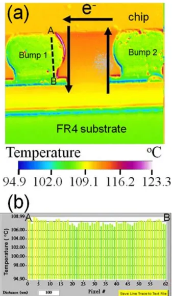
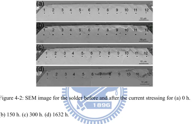
Figure 4-1: (a) IR images showing the temperature distribution in the bump with 0.6 A at 100 °C. (b) The temperature profiles along with dashed lines in the bump. 63 Figure 4-2: SEM image for the solder before and after the current stressing for (a) 0 h.
(b) 150 h. (c) 300 h. (d) 1632 h. ... 64
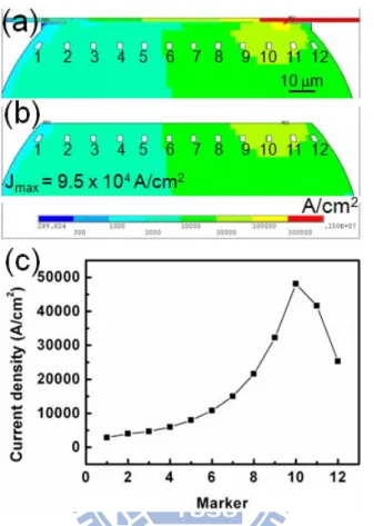
Figure 4-3: Simulation results on current density distribution in the flip-chip solder
xii
current density at the 12 marker positions. ... 65
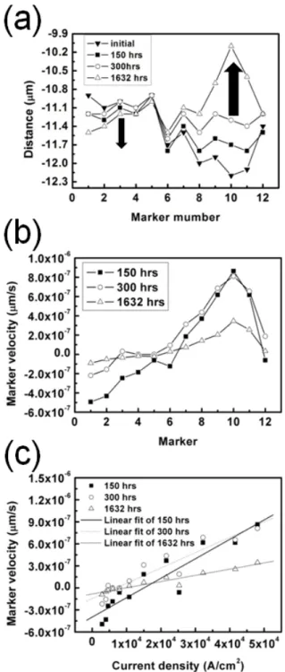
Figure 4-4: (a) The evolution of marker position for 12 markers at various stressing
times. (b) Marker velocity at 12 marker positions with different stressing time. (c)
Plot marker velocity as a function of local current density with different stressing
time. The marker velocity is proportional to the local current density at the
marker. ... 66
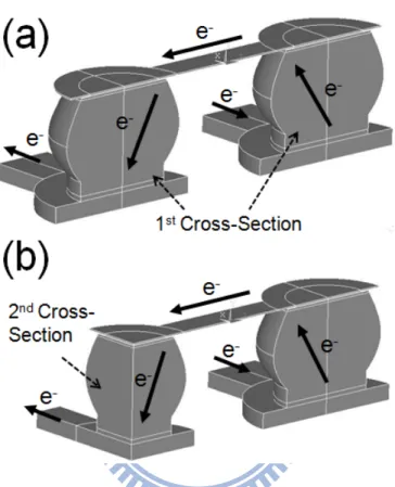
Figure 4-5: (a) Three-dimensional diagram for the solder joints with the direction of
electron flow with first cross-section. (b) Three-dimensional diagram for the
solder joints with the direction of electron flow with second cross-section. ... 74
Figure 4-6: Cross-sectional BEI for the solder joints with downward electron flow
before and after the current stressing. (a) Before current stressing. (b) After 150 h.
(c) After 1632 h current stressing. (d) Second cross-section for the sample in (c).
... 75
Figure 4-7: Cross-sectional BEI for the solder joints with upward electron flow before
and after the current stressing. (a) Before current stressing. (b) After 150 h. (c)
After 1632 h current stressing. (d) Higher magnification of the sample in (c) to
show a clear image of the whisker. ... 76
Figure 4-8: FIB image for second cross-section of the solder joints after the current
stressing for 1632 h. (a) In the solder bump with the upward electron flow. (b)
Higher magnification of (a) to show the grains and IMCs distributions of the
bump. (c) In the solder bump with the downward electron flow. (d) Higher
magnification of the sample in (c) to show the IMCs formation blocking the tin
diffusion path for the whisker growth. ... 77
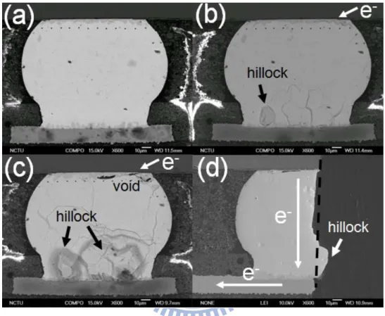
Figure 4-9: (a) Plan-view schematic of the layout design. Al trace connected all the
xiii
Cross-sectional diagram shows the experimental setup for (b) Approach 1. (c)
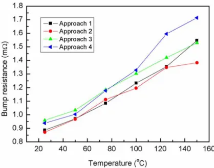
Approach 2. (d) Approach 3. (e) Approach 4. ... 89 Figure 4-10: The measured bump resistance as a function of temperature up to 150 °C for the four approaches. ... 90
Figure 4-11: (a) Simulation results shows the current density distribution across the
solder joints upon applying by 0.2 A. (b) The voltage distribution in the solder
joints. Voltage drop mainly occurred in Al trace. (c) Cross-sectional view along
the YZ plane in (b) shows that voltage drop inside the solder bump mainly
occurred at the high current density region. (d) Voltage distribution in the solder
joint, excluding Al trace and Cu line. Six positions were labeled for measuring
the voltage drop... 91
Figure 4-12: Three components contributing to the bump resistance, includ (a) Al disc,
(b) UBM/solder, (c) Cu disc. The resistance of Al disc contributed about 79% of
the total bump resistance. ... 92
Figure 4-13: Schematic drawings shows (a) the uniform current distribution and (b)
the current crowding effect in the solder joints. ... 93
Figure 4-14: Proposed layout of Kelvin structure for measuring bump resistance of the
flip-chip solder joint. ... 94
Figure 4-15: The voltage distribution in the solder bump when a void depleted
approximately 18% of the UBM opening. ... 94
Figure 4-16: Current density distribution in solder joints before void formation. (a)
Tilt view, shows solder bump only. (b) Cross-sectional view of (a). (c) Current
density distribution in solder adjacent to UBM/IMC layers. (d) Corresponding
cross-sectional view for temperature distribution. ... 103
xiv
shows solder bump only. (b) Cross-sectional view of (a). (c) Current density
distribution in solder adjacent to UBM/IMC layers. (d) Corresponding
temperature distribution. ... 104
Figure 4-18: Current density redistribution in solder joints at Stage II. (a) Tilt view,
shows solder bump only. (b) Cross-sectional view of (a). (c) Current density
distribution in solder adjacent to UBM/IMC layers. (d) Corresponding
temperature distribution. ... 105
Figure 4-19: Current density redistribution in solder joints at Stage III. (a) Tilt view,
shows solder bump only. (b) cross-sectional view of (a). (c) Current density
distribution in solder adjacent to UBM/IMC layers. (d) Corresponding
temperature distribution. ... 106
Figure 4-20: Current density redistribution in solder joints at Stage IV. (a) Tilt view,
shows solder bump only. (b) Cross-sectional view of (a). (c) Current density
distribution in solder adjacent to UBM/IMC layers. (d) Corresponding
temperature distribution. ... 107 Figure 4-21: Weibull distribution of the flip-chip solder joints with 40-μm-wide and
100-μm-wide Al traces. ... 117 Figure 4-22: (a) Changes in resistance of the six solder joints with 40-μm-wide Al
trace during electromigration tests. (b) Changes in resistance of the six solder joints with 100-μm-wide Al trace during electromigration tests. The insets in Fig. 2(a) and 2(b) show the enlargement of the resistance curve up to 95% of the
failure times. ... 118 Figure 4-23: Plan-view radiance-mode IR images of 40-μm-wide Al trace after 0.5 A current stressing at 165 °C. (a) First segment of Al trace. A serious damage occurred in Al pad of Bump 2. (b) Second segment of Al trace. (c) Third
xv
segment of Al trace. ... 119 Figure 4-24: Plan-view radiance-mode IR images of 100-μm-wide Al trace after 0.5 A current stressing at 165 °C. (a) First segment of Al trace. (b) Second segment of Al trace. (c) Third segment of Al trace. A serious damage occurred in the Al pad
for Bump 6. ... 120 Figure 4-25: Cross-sectional SEM images of six bumps with 40-μm-wide Al trace
after 0.5 A current stressing at 165 °C. (a) Bump 1 with upward electron flow. (b) Bump 2 with downward electron flow. Large voids were found in the chip side.
(c) Bump 3 with upward electron flow. (d) Bump 4 with downward electron flow.
(e) Bump 5 with upward electron flow. (f) Bump 6 with downward electron flow.
... 121 Figure 4-26: Cross-sectional SEM images of six bumps with 100-μm-wide Al trace
after 0.5 A current stressing at 165 °C. (a) Bump 1 with upward electron flow. (b) Bump 2 with downward electron flow. (c) Bump 3 with upward electron flow. (d)
Bump 4 with downward electron flow. (e) Bump 5 with upward electron flow. (f)
Bump 6 with downward electron flow. This bump has the most severe damage
among the six bumps. ... 122
Figure 4-27: Tilted view of cross-sectional current-density distribution in the solder bumps. (a) With 40-μm-wide Al trace. (b) With 100-μm-wide Al trace when they were stressed by 0.5 A. ... 123
Figure 4-28: Changes in resistance as a function of oven temperature. (a) For solder joints with 40-μm-wide Al trace. (b) For solder joints with 100-μm-wide Al trace. ... 124
Figure 4-29: Plan-view radiance-mode IR images of Al trace. (a) Before current
xvi
near Bump 2. ... 132
Figure 4-30: Cross-sectional SEM images of the solder bumps after open failure for (a)
Bump 1. (b) Bump 2. Melting behavior occurred in both bumps and
electromigration damage was observed at the chip side of Bump 2. ... 133
Figure 4-31: The measured resistance of the stressing circuit as a function of stressing
time. Abrupt increase in resistance took place at later stages of electromigration.
... 134
Figure 4-32: (a) The hot-spot temperature in the solder bumps as a function of the
depletion percentage of UBM opening due to void formation; (b) The hot-spot
temperature in the solder bump as a function of the resistance of Al trace.
Formation of voids was not considered in these results. ... 135
Figure 4-33: (a) IR images shows the temperature distribution. (b) The temperature
profiles along the dashed lines in the solder bumps. The red line shows the
non-linear distribution of the thermal gradient. ... 140
Figure 4-34: (a) Tilted view of three-dimensional current-density distribution in the
whole circuit. (b) Tilted view of three-dimensional temperature distribution in
the whole circuit. ... 141
Figure 4-35: (a) The cross-sectional temperature distribution in Bump 1. (b) Three
corresponding temperature profiles as defined in (a). ... 142
Figure 4-36: (a) The cross-sectional temperature distribution in Bump 2. (b) Three
corresponding temperature profiles as defined in (a). ... 143
Figure 5-1: The 3-D current density distribution in the solder joints with different UBM resistivity values (a) 295.4 μΩ⋅cm. (b)1477 μΩ⋅cm. (c) 2954 μΩ⋅cm. (d)14770 μΩ⋅cm. ... 150 Figure 5-2: The current density distribution inside the solder along Z-axis for the five
xvii
UBM resistivity values at the top layer of the solder (cross-section Y3). ... 151
Figure 5-3: Temperature distribution in the solder bumps when stressed by 0.567 A. (a) Standard model. (b) Solder joints with resistive UBM of 295.4 μΩ⋅cm. (c) Solder joints with resistive UBM of 1477 μΩ⋅cm. (d) Solder joints with resistive UBM of 2954 μΩ⋅cm. (e) Solder joints with resistive UBM of 14770 μΩ⋅cm (f) Simulated temperature in the solder joints as a function of applied current up to
0.567 A ... 152
Figure 5-4: The crowding ratios for Y1 to Y6 cross-sections for the effect of UBM
resistivity. ... 153
Figure 5-5: The simulation results shows the current density distribution under 0.6 A
in (a) Eutectic solder bump. (b) High-Pb solder bump. (c) Eutectic solder bump.
... 157
Figure 5-6: The simulation results shows the temperature distribution under 0.6 A in
(a) Eutectic solder bump. (b) High-Pb solder bump. (c) Eutectic solder bump. 158
Figure 5-7: The cross-sectional view of the results in Figure 5. (a) Eutectic solder
bump. (b) High-Pb solder bump. (c) Eutectic solder bump. ... 159
Figure 5-8: The four models constructed in this study. (a) The first model with a 34-μm-wide, 1.5-μm-thick and about 1000-μm-long Al trace. (b) The second model with a wider Al trace of 100 μm. (c) The third model with a thick Al trace of 4.4 μm. (d) The fourth model with a shorter Al trace of about 400 μm. ... 165 Figure 5-9: The cross-sectional views for the current-density distribution in the solder
bumps when they were stressed by 0.6 A. (a) The first model. (b) The second
model. (c) The third model. (d) The fourth model. ... 166
Figure 5-10: The cross-sectional views for the temperature distribution in the solder bumps when they were applied by 0.6 A at 70°C. (a) The first model. (b) The
xviii
second model. (c) The third model. (d) The fourth model. ... 167
Figure 5-11: (a) The hot-spot temperature. (b) The average temperature. (c) The
thermal gradient in the solder bumps as a function of applied current up to 0.6 A at 70 °C for the four models. ... 168 Figure 5-12: Current-density distribution in the solder joints with (a) 0.5-μm. (b)
5-μm. (c) 25-μm. (d) 50-μm. (e) 100-μm Cu UBM when applied by 0.6A. ... 174 Figure 5-13: Joule heating effect in Al trace for the solder joints with (a) 0.5-μm UBM. (b) 100-μm Cu column. ... 175 Figure 5-14: The temperature distribution in the solder bumps with (a) 0.5-μm. (b)
5-μm. (c) 25-μm. (d) 50-μm. (e) 100-μm Cu UBM when applied by 0.6 A at 100 °C. Only solder bump was shown. ... 176 Figure 5-15: The cross-sectional view for the temperature distribution in the solder
bumps with (a) 0.5-μm. (b) 5-μm. (c) 25-μm. (d) 50-μm. (e) 100-μm Cu UBM when applied by 0.6 A at 100 °C. Only solder bumps were shown. ... 177 Figure 5-16: Hot spot and average temperatures as a function of applied current up to 0.6A for the solder joints with (a) 25-μm. (b) 50-μm. (c) 100-μm Cu columns. The hot-spot was almost eliminated completely when the Cu column was thicker than 50 μm. ... 178 Figure 5-17: (a) Hot-spot temperature as a function of applied current for the five
models. The hot-spot temperature decreased as the thickness of Cu UBM
increased. (b) Average temperature in solder as a function of applied current for
the five models. No obvious increase in average temperature when the thickness
of Cu UBM was increased. ... 179
Figure 5-18: Thermal gradient as a function of applied current. Thick Cu UBM can
xix
Figure 5-19: The cross-sectional current density distribution of the solder bumps only with 10-μm-thick Cu UBM for different contact opening. (a) 30 μm in diameter. (b) 60 μm in diameter. (c) 85 μm in diameter. (d) 110 μm in diameter. ... 187 Figure 5-20: The enlarged cross-sectional current density distribution of the solder
joint with 10-μm-thick Cu UBM for different contact opening. (a) 30 μm in diameter. (b) 60 μm in diameter. (c) 85 μm in diameter. (d) 110 μm in diameter. ... 188
Figure 5-21: Maximum current density in the solder joints as a function of contact opening. (a) The solder joints with 1-μm-thick Cu UBM. (b) The solder joints with 5-μm-thick Cu UBM. (c) The solder joints with 10-μm-thick Cu UBM. (d) The solder joints with 25-μm-thick Cu UBM. ... 189 Figure 5-22: The optima contact opening for the solder joints as a function of UBM
thickness. ... 190
Figure 5-23: Cross-sectional view of current density distribution in the solder joints
for (a) Model 100%, (b) Model 80%, (c) Model 60%, (d) Model 40%, (e) Model
20%. When a current of 0.5 A was applied. ... 198
Figure 5-24: Plot of maximum current density in the solder bumps against the
diameter of UBM opening. ... 199
Figure 5-25: Plot of crowding ratio against the diameter of UBM opening. ... 200
Figure 5-26: The Joule heating effect in the solder joints for: (a) Model 100%, (b)
Model 80%, (c) Model 60%, (d) Model 40%, (e) Model 20%.When a current of 0.5 A was applied on 100 °C substrate. ... 201 Figure 5-27: Cross-sectional view of the temperature distribution in the solder bumps
for: (a) Model 100%, (b) Model 80%, (c) Model 60%, (d) Model 40%, (e) Model 20%. When a current of 0.5 A was applied and the substrate kept at 100 °C.
xx
Only the solder bumps are shown. ... 202
Figure 5-28: (a) Hot-spot temperature as a function of the applied current for the five
models. The hot-spot temperature increases as the bump size decreased. (b)
Average temperature in the solder as a function of the applied current for the five
models. The average temperature increases as the bump size was decreased. .. 203
Figure 5-29: Thermal gradient as a function of the UBM opening. Significant thermal
gradients were established when the solder size decreased. ... 204 Figure 5-30: The temperature distribution of Si die only for: (a) 50-μm-thick Si, (b) 75-μm-thick Si, (c) 150-μm-thick Si, (d) 300-μm-thick Si, (e) 500-μm-thick Si, (f) 750-μm-thick Si. When a current of 0.6 A was applied on 100 °C substrate. ... 209
Figure 5-31: The cross-sectional temperature distribution of the solder bumps only for: (a) 50-μm-thick Si, (b) 75-μm-thick Si, (c) 150-μm-thick Si, (d) 300-μm-thick Si, (e) 500-μm-thick Si, (f) 750-μm-thick Si. When a current of 0.6 A was applied on 100 °C substrate. ... 210 Figure 5-32: (a) Hot spot temperature in the solder joints as a function of die thickness.
xxi
List of tables
Table 3-1: The materials properties used in this study. ... 45
Table 4-1: The simulation voltages at the six positions in Figure 4-11 (b). ... 95
Table 4-2: Experimental and simulation results on bump resistances for the four
approaches. ... 95
Table 4-3: The resistance increases due to the void formation measured by the
different approaches in this study. ... 95
Table 4-4: The simulated maximum current density inside the solder, the
corresponding crowding ratio as well as the bump resistance at each stage. .... 108
Table 4-5: Electromigration reliability ... 125
Table 5-1: Maximum current density and crowding ratios at different cross sections
for the solder joints with various UBM with high resistivities. ... 154
Table 5-2: The simulation results on maximum current density, hot-spot and average
temperatures and thermal gradient for the high-Pb, eutectic SnPb and SnAg
solders. ... 160
Table 5-3: The maximum current density, hot-spot temperature, and estimated MTTF
for the five models in this section. ... 181
Table 5-4: Dimensions for the five simulation models in this section. ... 205
Table 5-5: MTTF Ratio for the five models stressed at 0.1 A to 0.5 A. MTTF for
1
Chapter 1 Introduction
1.1 Flip-chip technology
To meet the relentless drive for miniaturization of portable devices, flip-chip
technology has been adopted for high-density packaging due to its excellent electrical
characteristic and superior heat dissipation capability [1]. In 1960s, IBM first
developed the flip-chip technology, which was named as
controlled-collapse-chip-connection (C4) [2-4]. In C4 technology, high-Pb solder with
high melting temperature of 320 °C was used as solder joint material [5]. Then the
chip was aligned on the ceramic substrate and reflow soldering was performed to
form the solder joints. C4 technology gained wide utilization in 1980 since it can
provide a great number of advantages in size, performance, flexibility, reliability and
cost than other packaging methods. Owing to area array capability in flip-chip
technology, the size of entire die, the height of solder bump, and the length of
interconnect are effectively reduced, providing higher input/output (I/O) pin count
and signal propagation speed in electronic devices.
Before flip-chip assemblies, solder bumps need to deposit onto the under bump
metallurgy (UBM) on the chip side. The requirements for UBM are: (1) it must
2
passivation layer; (2) it is able to provide a sufficient barrier to prevent the diffusion
of other bump metals into the integrated circuit (IC); (3) it needs to be wettable by the
bump metals during solder reflow. For example, a thin film Cr/Cu/Au UBM is
adopted for the high-Pb solder alloy in C4 technology.
The typical of solder joints on silicon (Si) chip is shown in Figure 1-1 (a). Figure
1-1(b) is the schematic diagram of the cross-section of the flip-chip solder joints. As
depicted in Figure 1-1(c), the chip is then placed upside down (flip chip), and all the
joints are formed simultaneously between chip and substrate during the reflowing
process. In flip-chip process, electrical connections are the array of solder bumps on
the chip surface, hence interconnects distance between package and chip is effectively
reduced. The density of I/O is limited by the minimum distance between adjacent
bonding pads. For high ends device and when size reduction is the main concern,
area-arrayed flip-chip technology is the only choice to meet the needs.
However, flip-chip technology has some evolutions due to certain concern. In
order to cost down the consumer electronics, the polymer substrates, like
bismaleimide triazine (BT) or flame retardant 4 (FR4) printed circuit board, are used
to replace the ceramic substrate. For this concern, the high-Pb solder has no longer
been used due to its high melting point of 320 °C since polymers have relatively low
3
this problem for its low melting point of 183 °C. Next, owing to the environment
concern, the Pb-free solder alloys replace the Pb-containing solder alloys due to the
toxicity of Pb. Then, the thin film UBM will not be suitable for this change. Therefore,
the electroplating 5-μm Cu or 5-μm Cu/3-μm Ni was used as the UBM for the lead-free solder joints. Because of these evolutions, several kinds of solder alloys and
UBMs are able to select for the flip-chip assembly. This makes flip-chip technology
become complex since there are too many combinations. But the key is to find the
4
Figure 1-1: (a) Tilt-view of SEM image of arrays of solder bumps on silicon die. (b)
A flip-chip solder joint to connect the chip side and the module side. (c) The chip is
placed upside down (flip chip), and all the joints are formed simultaneously between
5
1.2 Electromigration
Electromigration (EM) has been the most persistent reliability issue in
interconnects of microelectronic devices. Electromigration is defined as mass
transport due to momentum transfer between conducting electrons and diffusing metal
atoms. For EM in a metal, the driving force acting on a diffusion atom consists two
forces: (1) the direct action of the electrostatic field on the diffusing atom,
electrostatic force, and (2) the momentum exchange between the moving electrons
and the ionic atoms, electron wind force. It can be expressed as [6]:
* * *
( )
el
direct wind wd
F =F +F =Z eE= Z +Z eE (1.1)
where Z* is the effective charge number, e is the electron charge, and E is the electric
field (E = ρj, where ρ is resistivity and j is current density). The effective charge Z*
includes two terms, Z*el and Z*wd. Z*el is nominal valence of the diffusing ions in the
metal when the dynamic screening effect is ignored. Z*eleE is named as direct force,
which draws atoms towards the electrode in negative bias. On the other hand, Z*wd,
represents the momentum exchange effect between electrons and the diffusion ions.
Generally speaking, the electron wind force, Z*wdeE, is dominant and is found to be
on the order of 10 for high conductivity metals such as Ag, Al, Cu, Pb. Sn, etc [7].
Z*wd can also be positive, but it was found that only in transition elements with
6 [8].
The atomic flux is related to the electric field and thus the current density. The
flux equation can then be expressed as the following:
* chem em dC D J J J D C Z eE dx kT = + = − + (1.2)
where C is concentration of diffusing species, D is the diffusivity, k is Boltzmann's
constant, and T is temperature.
After stressing for extended time, atoms in interconnects accumulate on the
anode end and voids appear on the cathode side, resulting in open failure eventually.
In general, the average drift velocity of atoms due to EM is given by Huntigton and
Grone [6]: j e Z kT D eE Z kT D C J v= = * = * ρ (1.3)
In 1976, the mass transport caused by EM was first observed in Al metal
interconnects. Figure 1-2 (a) is schematic diagram of Blech structure with a short Al
or Cu strip on a base line of TiN [9,10]. Because the resistance of Al or Cu is lower
than that of TiN, the current will take the lowest resistance path and go along the strip
of Al or Cu when the voltage bias is applied. After some period of time, a depleted
region occurs at the cathode and an extrusion occurs at the anode. Figure 1-2 (b) is the
top view of scanning electron microscope (SEM) image of a Cu strip tested for 99 hrs
7
Cu strip. In addition, from the mass conservation point of view, both depletion and
extrusion should have the same volume change. Thus, the drift velocity can be
calculated from the rate of depletion volume.
Figure 1-2: (a) A schematic diagram of typical EM behavior in a Al stripe. (b) SEM
images of the morphology of a Cu strip tested for 99 hrs at 350 °C with current
8
1.3 Electromigration behavior in flip-chip solder joints
In 1998, Brandenburg and Yeh first reported the EM failure in flip-chip solder
joints with eutectic SnPb [12]. In their research, some interesting observations were
found as follows: (1) the current density inducing in EM failure in the solder joints is
two order of magnitude lower than that in the Al; (2) the failure mode is pan-cake
type void formation in the cathode end; (3) the redistribution of Pb-rich and Sn-rich
phase was observed. Nowadays, to meet the higher demands for device’s performance,
the I/O numbers is expected to increase while the dimension of each individual joint
shrunks accordingly. To date, each bump measures at 100 μm or less in diameter. The design rule of packaging dictates that each bump is likely to carry current of 0.2 to 0.4
A. Due to this requirement, carry-on current density in the solder bumps must be
increased over 1 × 10⁴ A/cm2. This renders EM a daunting reliability issue in flip-chip
solder joints under such high current density [13]. In below, the four characteristics
for EM in flip chip solder joints will be thoroughly addressed.
1.3.1 Current crowding effect
Current crowding phenomenon is a unique behavior in flip-chip solder joints
under current stressing. However, the current crowding cannot be observed directly.
9
report by Yeh et al as shown in Figure 1-3 [14, 15]. It was found that the maximum
current density in a solder bump can be much higher than the average one that was
previously projected. It locates itself near the solder / UBM interface. Current
crowding occurs in solder joints is due to the current flow experiences a dramatic
geometrical and resistance transition from the thin on-chip metal line to the solder
bump. Because the cross-section of the Al trace on the chip side is about two orders
smaller than that of the solder joints, the majority of the current tends to gather near
Al-to-UBM entrance point to enter the solder bump instead of spreading uniformly
across the opening before entering the bump. The materials near the entrance point
experience a current density of about one order of magnitude higher than the average
value.
In previous study, Shao et al study the current density distribution in a solder
joint by a three-dimensional simulation [16,17]. Figure 1-4 (a) illustrates the typical
current density distribution in three-dimensions. From the cross-sectional view along
the Al trace of the whole bump, as shown in Figure 1-4 (b), the current crowds in the
solder bump near the entrance point of the Al trace. Also, from this study, the current
density distributions across six positions of the solder bump have been discussed.
Figures 1-5 (a) to (f) show the current density distribution of six layers for the UBM
10
and bottom layer of solder, respectively. The high current region for each layer is
close to the left hand side which is current entrance point. That means the current goes
from Al trace and through the shortest path in the solder joint, and then leaves through
the Cu line. It needs to note that the direction of current is opposite to electron charge
flow. Figures 1-6 (a) to (f) are the corresponding three-dimensional profile to Figures
1-5 (a) to (f). According to three-dimensional current density profile, it gives a clear
picture how the current distribute inside the solder joints.
“Crowding ratio” was used to define the degree of the current crowding effect.
Donation of “crowding ratio” is that the local maximum current density in the solder
joints divided by the average current density on the UBM opening.
Also, it is worth to mention that current crowding effect leads to non-uniform
current distribution inside a solder joint and in turn leads to non-uniform drift velocity
(see Section 1.2). The drift velocity is proportional to the current density and
non-uniform temperature distribution inside a solder joint due to local Joule heating
effect (see Section 1.3.2) [14]. As a result, EM-induced damage occurs near the
contact between the on-chip line and the bump; voids formation for the bumps with
electrons downward and hillock or whisker for the bumps with electrons upward.
Therefore, current crowding effect plays a crucial role in the flip-chip solder joints
11
Figure 1-3: (a) Unique line-to-bump geometry of a flip-chip solder bump joining an
interconnect line on the chip side (top) and a conducting trace on the board side
(bottom). (b) Two-dimensional (2D) simulation of current distribution in a solder joint.
12
Figure 1-4: (a) 3D current-density distribution in the solder joint with the
Ti/Cr–Cu/Cu thin-film UBM. (b) Current-density distribution at the Z-axis cross
section in (a). The black dotted lines show the six cross-sections examined in this
13
Figure 1-5: The plan-view current-density distribution at different cross-sections: (a)
Cross-section Y1, which is located inside UBM. (b) Cross-section Y2, which is IMC
layer.(c) Cross-section Y3, which is the top layer of the solder connected to IMC
formed between UBM and the solder.(d) Cross-section Y4, which is the largest
diameter in the joints. (e) Cross-section Y5, which is a smaller diameter due to solder
mask process. (f) Cross-section Y6, which is situated at the bottom of the solder joint.
14
Figure 1-6: The three-dimensional current-density distribution at the different
cross-sections: (a) Cross-section Y1, which is located inside the UBM. (b)
Cross-section Y2, which is the IMC layer.(c) Cross-section Y3, which is the top layer
of the solder connected to the IMC formed between the UBM and the solder.(d)
Cross-section Y4, which has the largest diameter in the joints. (e) Cross-section Y5,
which has a smaller diameter due to solder mask process. (f) Cross-section Y6, which
15
1.3.2 Joule heating effect
When the current flow pass through a conductor, heat is generated due to the
electrons colliding the atoms in the conductor. This is so called Joule heating effect.
The heating power can be describe as:
V j R I
P= 2 = 2ρ (1.4)
where P is the heating power, I is the applied current, R is the resistance of the
conductor, j is the current density, r is the resistivity of the conductor, and V is the
volume of the conductor. Thus, the heating is influenced by two factors: the applied
current and the resistance of the conductor.
When the flip-chip solder joints are applied with high currents, a lot of heat
generates. Furthermore, the total length of Al trace is typically about few hundreds to
few thousands micrometers, which corresponds to a resistance of approximately few
ohms. In contrast, the resistances of the solder bumps and the Cu trace in the substrate
are relatively low, typically in the order of few or tens of milliohms. Therefore, the
primary contributor for Joule heating in the solder joints is Al trace [18-20]. Al trace
is the main heating source. As a result, the temperature in the bumps during
accelerated testing is likely to be much higher than that of the ambient because of the
Joule heating. Moreover, the current crowding effect leads to the local high current
16
temperature distribution becomes non-uniform in the flip-chip solder joints. Also,
Chiu et al reported the “hot spot” exists in the solder bumps at the crowding region
[20, 21]. The combination of the Joule heating of Al interconnects on the chip side
and the non-uniform current distribution will lead to a temperature gradient across the
solder joints. Consequently, Joule heating effect induced the increasing in temperature
in the flip-chip solder joints under EM significantly affects the analysis of failure time
(see Section 1.3.4).
1.3.3 Void formation and propagation
Voids formation and propagation at the cathode end is the typical EM failure
mode of electromigration in flip-chip solder joints. For flip-chip solder joints with a
thin film UBM, the current crowding effect leads to a pancake-type of void formation
near the entrance point of the current flow and the void propagates along the interface
of intermetallic compound (IMC) and solder [13, 14, 22-29]. Figure 1-7 (a) displays
the SEM images of eutectic SnPb after EM [13, 14]. After stressing at 125 °C / 2.25 ×
104 A/cm2 for 40 h, voids formed in the upper left-hand corner since electron flow
entered the bump from the left-upper corner of the joint. Similar phenomena were also
observed in Sn-4.0Ag-0.5 Cu Pb-free solder joints as shown in Figure 1-7 (b) [24].
Pancake-type void is clearly seen at the corner of flip-chip solder joints when the
17
propagate across the top of solder joints, resulted in open failure. Later, the
re-distribution of current density and temperature due to void formation and
propagation will be discussed.
Figure 1-7: (a) SEM images of a sequence of void formation and propagation in a
flip-chip eutectic SnPb solder bump stressed on 125 °C at 2.25 × 10⁴ A/cm2 for 40 h.
(b) SEM image of void formation in flip-chip 95.5Sn-4.0Ag-0.5Cu solder bump on
18
1.3.4 Mean-Time-To-Failure (MTTF)
For EM to occur, a non-vanishing divergence of atomic flux is a requirement.
Since electromigration damage is cumulative, it affects the failure rate. In statistic
study, the test samples should be stressed at the same current and temperature
conditions. Then, the failure time or lifetime can be recorded and plot by Weibull or
normal distribution. In Weibull distribution, 63.2% of the time of unreliability is
denoted as the MTTF [30]. In 1969, J. R. Black explained the MTTF in the presence
of EM which was given by the equation [31]:
⎟ ⎠ ⎞ ⎜ ⎝ ⎛ = kT Ea J A MTTF 1n exp (1.5)
where A is a constant, J is current density, n is a model parameter, Ea is activation
energy, k is Boltzmann’s constant, and T is average temperature. There are four
parameters, j, n, Ea, and T. All of them need to be examined and analyzed. However,
current crowding effect and Joule heating effect in the flip-chip solder joints play
important roles under EM. To include these effects in MTTF analysis, Black’s
equation needs to be modified by multiplying J with a crowding ratio c and add T as
an increment of ΔT due to Joule heating [15]:
( )
(
)
⎥ ⎦ ⎤ ⎢ ⎣ ⎡ Δ + = T T k Ea cJ A MTTF 1 n exp (1.6)For the following discussion, the estimated MTTF will be a key result to
19
1.4 Thermomigration
Thermomigration is defined as a flow of mass driven by a temperature gradient
[8,32]. In most metallurgical process, when we anneal an inhomogeneous binary alloy
in a furnace at a constant temperature and constant pressure, the alloy tends to become
homogenous. On the other hand, if we anneal a homogeneous binary alloy under a
temperature gradient, i.e., if one end of it is hotter than the other end, the
homogeneous alloy will become inhomogeneous. This phenomenon is named Soret
effect or thermomigration, which explains the uphill diffusion for one element and
downhill diffusion for another element in a solid solution after being exposed to a
temperature gradient. Thermomigration can occur in a pure metal or binary eutectic
alloy. For example, Soret effect has been reported to occur in a solid solution of PbIn
alloy [33, 34].
When a temperature gradient is established, energy and momentum of the
electrons at high temperature side is greater than that at low temperature side. The
gradient in the momentum exchange produces a driving force for relative movement
of the components [35]. In addition, concentration of equilibrium should also be
considered in thermomigration. Since a temperature gradient exists, the concentration
of equilibrium at high temperature is higher than that at low temperature side. Thus,
20
movement of the component. Here, the driving force exerted by the temperature
gradient can be expressed as
dx dT T Q F * = (1.7)
where Q* is defined as heat of transport, which is different between heat carried by a
moving atom per mole to the heat of atoms per mole at the hot end and T is
temperature [36]. Q* can be positive or negative, depends on the direction of
component movement. Q* is the positive sign when the flux is from cold to hot region,
which means the component gains heat. Q* stand for negative when the component is
from hot to cold region. The flux equation of thermomigration is given as
(
)
⎟ ⎠ ⎞ ⎜ ⎝ ⎛ ∂ ∂ − = x T T N Q kT D C J / * (1.8)where C is concentration, D is diffusivity, N is Avogadro number, and kT is thermal
energy. It is worth mentioning that D is the isothermal diffusion coefficient. The jump
mechanism or mean jump frequency is not change by the temperature gradient at any
temperature. However, it biases the direction of jumps.
Thermomigration of flip chip solder joints under current stressing was first
reported by Ye et al. [18]. According to their results, several voids were found on
these two bumps near the Si chip side. Voids formation on one bump was more
serious than that on another bump, as shown in Figure 1-8. EM alone can not explain
21
current direction would not have void formation near the chip side at the same time.
Therefore, thermomigration combined with EM occurred in this pair of solder bumps,
as further proved by the marker movement. In Figure 1-9, three-dimensional
thermo-electrical finite elements simulation model was used to simulate the
temperature distribution from the surface of chip side to the bottom of the solder
joints. Their results indicate that a linear temperature gradient of 1500 °C/cm is
predicted. This linear temperature gradient of 1500 °C/cm seems sufficient to cause
thermomigration in eutectic SnPb solder joints.
Later, thermomigration in SnPb composite flip-chip solder joints at an ambient
temperature of 150 °C was observed [37,38]. Figure 1-10 shows the SEM images of
composite solder joints before and after thermomigration. The redistribution of Sn and
Pb occurs due to a temperature gradient with Sn atoms moved to hot end and Pb
atoms moved to cold end. From our previous research [37, 38], we performed the
analysis of phase separation mechanism to estimate the driving force of
thermomigration assumed 10 °C difference across a solder joint of 100 μm. That means a linear temperature gradient of 1000 °C/cm will induce thermomigration in
the solder joints.
From studies above, they assumed that the thermal gradient in the solder joints is
22
was found by Chiu et al. [20]. More detail studies should be done on this part to
confirm the distribution of the thermal gradient. Since there exists the non-linear
thermal gradient exists in the solder bumps, it will impact the analysis of the study of
23
Figure 1-8: The formation of voids on the chip side and accumulation of solder on the
substrate side for the solder bump with. (a) Downward electron flow. (b) Upward
24
Figure 1-9: (a) Temperature distribution on the solder bump. (b) Temperature
25
Figure 1-10: SEM image of composite flip-chip solder bump. (a) As prepared. (b)
26
1.5 Motivations
The current that each solder bump needs to carry continually increases. In
addition, the miniaturization trend in portable microelectronic products drives the
shrinkage of the dimension of solder bumps, which caused in a dramatic increase of
current density in solder joints. Therefore, EM has become an important reliability
issue of flip-chip solder joints.
The two key issues in flip-chip solder joints under EM are the current density
and the temperature distributions inside the solder bumps. However, they are hard to
measure directly. In the study, the three-dimensional finite elements method is
adopted to analysis the thermo-electrical characteristics in the solder joints. Also, the
experiment was performed to confirm the simulation results. The experimental results
of thermo-electrical characterization on the EM of the solder joints include the
observation of current crowding phenomena by marker movement, the bump
resistance by the design of Kelvin probe, the effect of the width of Al trace on MTTF,
the effect of Al trace degradation on Joule heating, and non-linear distribution of
thermal gradient. In addition, the current density and temperature re-distribution due
to void formation and propagation will be discussed. Moreover, by simulation, the
prediction to enhance EM resistance, i.e. relieving the current crowding effect and
27
UBM materials, solder alloys, Al-trace design, UBM thickness, and size of contact
opening. Finally, the shrinkage of solder bump size and die thickness are investigated
since the 3D IC packaging becomes more and more important for next packaging
28
Chapter 2 Experimental procedure
2.1 Sample preparation
Three kinds of flip-chip samples were used in the EM test in this study. The
samples prepared by typical bumping process including photolithography, Cu and
solder electroplating, flip-chip reflow process and etc. First, the solder joints were
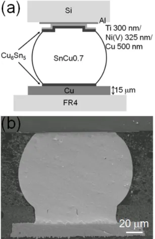
eutectic SnPb solder with a tri-layer 0.1 μm Ti / 0.3 μm Cr-Cu/ 0.7 μm Cu UBM provided by APack [39] as illustrated in Figure 2-1 (a). The SEM image of solder
joints from APack as prepared is shown in Figure 2-1 (b). Passivation and UBM
openings were 85 and 120 μm in diameter respectively. Al trace on the chip side was 34 μm wide and 1.5 μm thick. Cu line on the BT substrate was 80 μm wide and 25 μm thick. The height and pitch of the bump are 145 and 400 μm, respectively. Dimension of Si chip was 7.0 × 4.8 mm2 and the thickness was 290 μm, whereas the
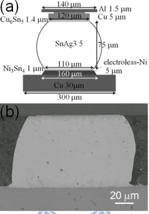
dimension of BT substrate was 5.4 mm wide, 9.0 mm long and 480 μm thick. Second, Lead-free SnAg3.5 solder joints were adopted and the UBM is 0.5-μm Ti-Cu/5-μm Cu. This kind of sample is provided by Megic [40]. The schematics and SEM image
of the solder joint samples from Megic is shown in Figures 2-2 (a) and (b),
respectively. The 0.5-μm Ti-Cu was sputtered as a Cu seed layer, and then a 5-μm Cu layer was electroplated. The diameter of the UBM opening was 120 μm. Lead-free SnAg3.5 solder bumps were electroplated and joined to FR5 substrates. The bump
29
height was about 75 μm. The metallization layer on the FR5 substrate was a 5-μm electroless-Ni. The dimension of the Cu pad opening in the substrate was 300 μm in diameter. Al trace on the chip side was 100 μm or 40 μm wide and 1.5 μm thick. Cu line on BT substrate was 100 μm wide and 25 μm thick. The bump height and pitch are 75 and 800 μm, respectively. Third, the test vehicle employed in the EM study was a flip-chip package, that is a Si chip interconnected to the substrate by an array of
Pb-free solder joints. In the drawing Figure 2-3 (a), all these samples are FCBGA
flip-chip packages provided by ASE [41]. The pitch between adjacent solder joints is
270 μm. The bump height is about 100 μm. Figure 2-3 (b) is a cross-sectional view of a flip-chip solder joint by SEM image. The UBM on the chip side is a tri-layer thin
film of Ti/Ni(V)/Cu. The thickness of the Cu thin film is 0.5 μm. The diameter of UBM opening and passivation opening were 110 and 85 μm, respectively. Printing solder of Sn-0.7Cu alloy was used on the chip side. The substrate metallization on Cu
bond-pad features the solder-on-pad (SOP) surface treatment, i.e., with printed
Sn-3.0Ag-0.5Cu pre-solder on Cu bond-pad surface. Cu bond-pad has a thickness of
15 μm, which is much thicker than Cu thin film UBM on the chip side. The printing solder and the SOP were reflowed together and became the Pb-free bumps. The stress
30
Figure 2-1: (a) The cross-sectional schematic shows the flip-chip solder joints from
APack. (b) The cross-sectional SEM image of flip-chip solder joints as prepared by
31
Figure 2-2: (a) The cross-sectional schematic shows the flip-chip solder joints from
Megic. (b) The cross-sectional SEM image of flip-chip solder joints as prepared by
32
Figure 2-3: (a) The cross-sectional schematic shows the flip-chip solder joints from
ASE. (b) The cross-sectional SEM image of flip-chip solder joints as prepared by
33
2.2 Automated data acquirement system
In this study, power supply Keithley 2400 [42] and power supply Agilent
E3646A [43] are served as the current sources. Data switch Agilent E34970A [43]
with three pieces of 20-channels modulus was used to monitor the voltage history.
The limitation of the voltage measurement is about 5 μV for the power supply and the data switch. Since the initial EM failure of the flip-chip solder joints may increase
several micro-ohm of resistance, this measuring system can provide enough accuracy
for our measurement. To fit long time current stressing in EM tests, an in-house
controlling software was encoded by LabVIEW [44,45]. Using the software, the
stressing current, stressing time and failure criteria can be easily recorded. To link the
apparatus and the software, the GPIB card from NI [44] was employed to serve the
long time, stable, and precise controller. The measuring system is illustrated in Figure
34
35
2.3 Microstructure examination
Cross-sectional and whole-bump samples were prepared for the EM test. The
cross-sectional samples were first polished to the half solder joints before current
stressing. After stressing the whole-bump samples, the samples also need to be ground
and polished to certain position. The following apparatus or equipments were used to
inspect the morphology and the composition changes of the solder joints.
2.3.1 SEM
In Figure 2-5 (a), JEOL JSM-6500F and JEOL JSM-6700F field-emission
scanning electron microscopy (FESEM) were used for the examination of EM
damage. The high-voltage electron-beam hits the samples on the stage, and then
releases the secondary electrons. By collecting the secondary form the surface of the
samples, the secondary electron images (SEI) can be acquired to analysis the surface
morphology. On the other hand, backscattered electrons are beam electrons that
reflected from the sample by elastic scattering. Backscattered electrons are often used
in analytical SEM along with the spectra of characteristic x-rays. Because the
intensity of the backscattered electrons signal is strongly related to the atomic number
(Z) of the specimen, backscattered electrons images (BEI) can provide information
36
2.3.2 Energy dispersive spectroscopy (EDS)
The detector of energy dispersive X-ray spectroscopy (EDS) attached to SEM is
adopted to analyze the compositions of the flip-chip solders joints. A detector was
used to convert X-ray energy into electrical signals. As the energy of the X-rays is
characteristics of the difference in energy between the two shells and of the atomic
structure of the element from which they were emitted, this allows the elemental
composition of the specimen to be detected.
2.3.3 Focused ion beam (FIB)
Figure 2-5 (b) depicts the dual-beam focused ion beam (DB-FIB) of FEI
Nova-200 used for the examination. The FIB can be utilized for precise cutting,
selective deposition, selective etching, and TEM samples preparation. In this study,
the precise cutting, selective etching, and the ion channeling image were used by FIB.
Due to ion channeling effect, the contrast of grain orientation looks different since
different grain orientation has different ion channeling. If the orientation is parallel
with the ion direction, it looks darker under ion channeling. Otherwise, when the grain
37
38
2.4 Temperature measurement
Since the Joule heating effect is a major issue in this study, how to measure the
accurate temperature distribution is the key problem to be solved. The thermal couple
may be used to measure the temperature. However, the contact point of thermal
couple is too large to measure the exact temperature in flip-chip solder joints. In this
study, the following two methods are employed to obtain the temperature in the
flip-chip solder joints without damaging the samples.
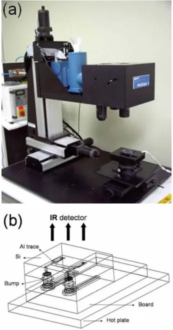
2.4.1 Infrared microscopy
An infrared microscope (IR) form Quantum Focus Instrument (QFI) as shown in
Figure 2-6 (a) was employed to measure the temperature in the flip-chip solder joints
under current stressing [21]. The temperature distribution inside the bumps was
detected by a thermal infrared microscope, which the resolution of 0.1 °C in
temperature sensitivity and 2.8 μm in spatial resolution per pixel. Before the current stressing, the emissivity of the specimen was calibrated at 100 °C. After the
calibration, the bumps were stressed by a desired current condition. Then, temperature
measurement was performed to record the temperature distribution after the
temperature reached a steady state. Figure 2-6 (b) shows the schematic diagram for
experimental setup, in which the Si side faces the infrared microscope. Since the 250
39
m and much larger than the thickness of the Si wafer. Therefore, the absorption of Si
chip can be ignored [46]. Another purpose to use IR is it can be used to detect the
materials distribution by the radiance mode. The radiance of a metal is smaller than
that of a ploymer. Thus, the metal appears brighter in the image.
Figure 2-6: (a) The photograph of the IR microscope. (b) The schematic diagram for
40
2.4.2 Thermal sensors by TCR effect of Al lines
The temperature coefficient of resistance (TCR) is a physical property of metals.
Since the electrical resistance of a metal conductor such as a copper wire is dependent
upon collision processes within the wire, the resistivity could be expected to increase
with temperature since there will be more collisions. An intuitive approach to
temperature dependence leads one to expect a fractional change in resistance which is
proportional to the temperature change:
(
)
[
o]
o T T
R
R= 1+α − (2.1)
where R is the resistance at temperature of interest, Ro was the reference resistance, α
is the temperature coefficient of resistance, T is the temperature of interest, and To is
the reference temperature.
To explore the TCR effect, the layout in Figure 2-7 is designed as a thermal
sensor in the flip-chip solder joints. For the TCR calibration, the applied current was
0.2 A through pad 1 to pad 2 in the oven. The voltage drop was monitored through
pad 3 and pad 4. Thus, the measured resistance included the resistance of bump 3 and
bump 4, some Cu lines, as well as the resistance of the Al trace connecting bump 3
and bump 4. To calibrate the TCR, the resistance was measured in an oven in which
the temperature was from 50 to 175 °C. After calibration, the exact bump temperature