High-power AlGaInP light-emitting diodes with metal substrates fabricated by wafer
bonding
Wei Chih Peng and YewChung Sermon Wu
Citation: Applied Physics Letters 84, 1841 (2004); doi: 10.1063/1.1682696 View online: http://dx.doi.org/10.1063/1.1682696
View Table of Contents: http://scitation.aip.org/content/aip/journal/apl/84/11?ver=pdfcov Published by the AIP Publishing
Articles you may be interested in
GaInN light-emitting diodes using separate epitaxial growth for the p-type region to attain polarization-inverted electron-blocking layer, reduced electron leakage, and improved hole injection
Appl. Phys. Lett. 103, 201112 (2013); 10.1063/1.4829576
AlGaInP/mirror/Si light-emitting diodes with vertical electrodes by wafer bonding Appl. Phys. Lett. 82, 4011 (2003); 10.1063/1.1579132
Evidence for voltage drops at misaligned wafer-bonded interfaces of AlGaInP light-emitting diodes by electrostatic force microscopy
J. Appl. Phys. 90, 4791 (2001); 10.1063/1.1406549
AlGaInP light-emitting diodes with mirror substrates fabricated by wafer bonding Appl. Phys. Lett. 75, 3054 (1999); 10.1063/1.125228
AlGaInP/AuBe/glass light-emitting diodes fabricated by wafer bonding technology Appl. Phys. Lett. 75, 154 (1999); 10.1063/1.124303
This article is copyrighted as indicated in the article. Reuse of AIP content is subject to the terms at: http://scitation.aip.org/termsconditions. Downloaded to IP: 140.113.38.11 On: Thu, 01 May 2014 04:27:59
High-power AlGaInP light-emitting diodes with metal substrates fabricated
by wafer bonding
Wei Chih Peng and YewChung Sermon Wua)
Department of Materials Science and Engineering, National Chiao Tung University, Hsinchu 300, Taiwan, Republic of China
共Received 28 July 2003; accepted 20 January 2004兲
High-power light-emitting diodes 共LEDs兲 fabricated on Cu substrates were investigated in this study. The AlGaInP LED structure was bonded to a Cu substrate by using indium-tin-oxide as the diffusion barrier layer. It was found that Cu-substrate-bonded LED devices could be operated in a much higher injection forward current, 800 mA, which was eight times higher than that used in traditional GaAs-substrate LEDs. The luminous intensity of the Cu-substrate LEDs could reach as high as 1230 mcd, which was three times higher than that of the GaAs-substrate LEDs. © 2004
American Institute of Physics. 关DOI: 10.1063/1.1682696兴
The epitaxial growth techniques have significantly im-proved the brightness and efficiency of light-emitting diodes 共LEDs兲. LEDs operating in the wavelength region ranging from red to green light have been employed by the AlGaInP alloy system grown on GaAs substrates.1However, its use in high-efficiency applications has been limited because of the substrate absorption and the internal reflection. Fortunately, the wafer bonding process can solve these problems.2–7 Nev-ertheless, despite improving luminous efficiency, LED sources are limited to use in low power applications due to the low thermal conductivity of the substrate. To achieve higher light output performance, it is necessary to drive the LED at a higher current. In this study, AlGaInP LEDs with wafer-bonded metal共Cu兲 substrates were proposed. The per-formance of the Cu-substrate LEDs was also been investi-gated.
The AlGaInP multiple quantum well共MQW兲 LED struc-tures were grown on GaAs substrates through low-pressure metalorganic chemical vapor deposition. The LED structure consisted of an n-GaAs buffer layer, an n-InGaP etching stop layer, an n-GaAs ohmic contact layer, an AlInP
n-cladding layer, an undoped (Al0.15Ga0.85)0.5In0.5P MQW active region, an AlInP p-cladding layer, and a p-GaP win-dow layer. An ITO layer was deposited on the AlGaInP LED to act as a current-spreading layer. On the other hand, the host Cu substrate played the role of a heat sink substrate. These two wafers were cleaned and then placed in contact with each other immediately using a designed fixture8 that ensured uniform pressure on each of the wafers. Then, the fixture was loaded into a furnace and annealed at tempera-tures varying from 400 to 600 °C for 30 min in argon ambi-ent. After the wafers were allowed to cool to room tempera-ture, the GaAs substrate and the InGaP layer were removed by chemical etching in solutions of 1NH4OH:10H2O2 and
1HCl:10H2O, respectively. The fused epilayer was
mesa-etched into isolated devices with 250⫻250m2 area. The Au/AuGe dots with a diameter of 100 m were deposited onto the n-side (n⫹-GaAs contact layer兲 and then alloyed for
ohmic contact metalizations. It should be noted that the Cu substrate is a conductor, which can act as p-side contact; thus it is not necessary to deposit any metal for p-side contact. In comparison, the LED samples with the GaAs and Cu sub-strates were prepared from the same AlGaInP LED epitaxial material, and the samples described here were only cut into chips without encapsulation before electrical and optical measurements.
Figure 1共a兲 shows a successful LED wafer bonded on a Cu substrate at 500 °C for 30 min. After removing the GaAs
a兲Author to whom correspondence should be addressed; electronic mail: [email protected]
FIG. 1. 共a兲 A successful Cu-substrate-bonded LED sample and 共b兲 a scan-ning electron micrograph of the cross section of the LED structure.
APPLIED PHYSICS LETTERS VOLUME 84, NUMBER 11 15 MARCH 2004
1841
0003-6951/2004/84(11)/1841/3/$22.00 © 2004 American Institute of Physics
This article is copyrighted as indicated in the article. Reuse of AIP content is subject to the terms at: http://scitation.aip.org/termsconditions. Downloaded to IP: 140.113.38.11 On: Thu, 01 May 2014 04:27:59
substrate, no peeling or cracks were observed on the mirror-like surface despite the large difference between the thermal expansion coefficients of GaAs (6.86⫻10⫺6/°C) and Cu (16.8⫻10⫺6/°C). The fused epilayer then was mesa-etched into isolated devices, deposited with contact dots, and then alloyed for ohmic contact metalizations.
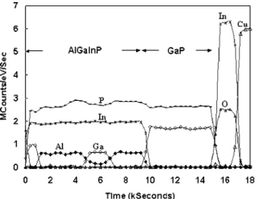
Figure 1共b兲 shows the cross-section image of this bonded LED structure. Neither cavity nor unbonded area was found on the bonded interface. The Aauger depth profiles of Al-GaInP LED/ITO/Cu substrate are shown in Fig. 2. It revealed no Cu element diffused into the AlGaInP active layer of LEDs structure. For the purpose of comparison, an indium-tin-oxide 共ITO兲-free AlGaInP LED substrate was also bonded to Cu substrate at the same condition. The Cu ele-ment was found to diffuse into the AlGaInP LED structure and destroy the LED structure. The results indicated that the ITO layer employed here not only acted as a current spread-ing layer but also a barrier layer.
When ITO film was used as the bonding layer, it was also found that the bonding temperature would affect the yield of the Cu-substrate LEDs. The sample did not bond at temperatures below 400 °C. At temperatures greater than 400 °C, the bonded area increased when temperature in-creased as a result of both the reaction and diffusion rates increasing with temperature. However, when bonding tem-perature reached 600 °C, the Cu element could penetrate through the ITO layer and destroy the LED structure.
Figure 3 presents the current versus voltage (I – V) of the Cu-substrate LEDs bonded at 500 °C for 30 min. The device exhibited normal p – n diode behavior with a forward voltage of 1.96 V at 20 mA, which was similar to that of GaAs-substrate LEDs. This indicated that the wafer-bonding pro-cess did not degrade the performance of LEDs. It is worthy to note that the series resistance of Cu-substrate LED 共1–2 ⍀兲 is lower than that of GaAs-substrate LED 共5–7 ⍀兲.9
The effects of heat sink observed in high power LEDs are very important with regard to the removal of heat from LED devices. The performance of the LEDs would otherwise degrade when the operation temperature increased. Figure 4 shows the peak spectral wavelength as a function of the dc drive current. During the test conditions, these two LED
samples, which had been cut into chips without encapsulat-ing, were put on a metal chunk. The data show that the emission peak wavelengths shift toward longer wavelengths with increasing dc drive current, which is caused by the joule heating. Unlike the 4 nm redshift exhibited at 170 mA in GaAs-substrate LEDs, the Cu-substrate LED devices exhib-its a more favorable 2 nm redshift. The redshift of the emis-sion wavelength occurred as the temperature increased. From the shift in emission wavelength and a wavelength shift with temperature of 0.096 nm/°C for 620 nm AlGalnP LEDs,10it could be estimated that the thermal resistance of the Cu-substrate LEDs was approximately 60 °C/W smaller than that of substrate LEDs. Thus the temperature of GaAs-substrate LEDs was about 20 °C higher than that of the Cu-substrate LEDs at 170 mA.
Figure 5 shows the effects of injection current on the luminous intensity of the LEDs. When the injection current was less than 100 mA, the luminous intensities of two samples were the same, meaning that the wafer-bonding
pro-FIG. 2. Auger depth profiles of AlGaInP LED/ITO-Cu sample bonded at 500 °C for 30 min.
FIG. 3. Current–voltage characteristic of the Cu-substrate-bonded LED de-vices fabricated by wafer bonding technology.
FIG. 4. Peak spectral wavelength against dc injection current for the LEDs with a GaAs substrate and a Cu substrate.
1842 Appl. Phys. Lett., Vol. 84, No. 11, 15 March 2004 W. C. Peng and Y. S. Wu
This article is copyrighted as indicated in the article. Reuse of AIP content is subject to the terms at: http://scitation.aip.org/termsconditions. Downloaded to IP: 140.113.38.11 On: Thu, 01 May 2014 04:27:59
cess did not degrade the performance of Cu-substrate LEDs. When the injection current reached 100 mA, the GaAs-substrate LEDs were saturated. However, the intensity of the Cu-substrate LEDs did not saturated at 100 mA. The maxi-mum luminous intensity of Cu-substrate LEDs could reach as high as about 1230 mcd at 800 mA, which was three times higher than the saturation intensity of the GaAs-substrate LEDs at 100 mA.
These results were due to a much smaller series resis-tance of the Cu-substrate LEDs as compared with GaAs-substrate LEDs, thereby reducing the total amount of joule heating. Since the reduction of the joule heating would in-crease the quantum efficiency of the LEDs, the Cu-substrate LEDs had a smaller redshift, and could be driven at a higher current and therefore obtain a higher luminous intensity. This difference might also be a result of the disparity between their respective thermal conductivities; the thermal conduc-tivity of Cu 共401 Wm⫺1K⫺1兲 is nine times higher than that of GaAs 共46 Wm⫺1K⫺1兲. Therefore, by using these wafer bonding techniques, the joule-heating problem in conven-tional LEDs can be significantly reduced.
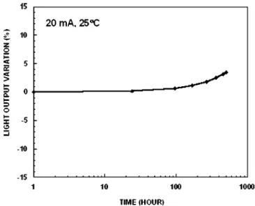
The other important issue of the Cu-substrate LEDs is the reliability. Copper is an impurity long known to cause strong degradation in LEDs.11 The efficiency of Cu-contaminated LEDs would significantly decreased after life test. In this study, the life test of Cu-substrate LEDs was performed at forward current of 20 mA in room temperature, corresponding to 32 A/cm2. As shown in Fig. 6, the degra-dation of the luminescence-output intensity was less than 5% after 500 h of life test.
In summary, high-power Cu-substrate LEDs fabricated by bonding AlGaInP LED structure to Cu substrate were investigated in this study. An ITO film was used as an inter-mediate layer to bonded wafers. It was found that the sample did not bond at temperatures below 400 °C. When bonding temperature reached 600 °C, the Cu element diffused through the ITO layer and destroyed the LED structure. Fortunately,
Cu did not penetrate the ITO layer when samples were bonded at 500 °C for 30 min, and the high-power Cu-substrate LEDs were successfully fabricated. In Cu-Cu-substrate LEDs, the joule heating exhibited in conventional GaAs-substrate LEDs was significantly reduced because the Cu substrate has larger thermal conductivity and lower thermal resistance as compared with GaAs substrate. It was found that Cu-substrate LEDs could be operated in a much higher injection forward current, 800 mA, which was eight times higher than that used in GaAs-substrate LEDs. The luminous intensity of the Cu-substrate LEDs could reach as high as 1230 mcd, which was three times higher than that of the GaAs-substrate LEDs.
This project was funded by Epistar Corporation and Na-tional Science Council共NSC兲 of the Republic of China under grant No 92-2216-E-009-012.
1F. A. Kish, F. M. Steranka, D. C. Defevere, D. A. Vanderwater, K. G. Park, C. P. KuoM, and G. Craford, Appl. Phys. Lett. 64, 2839共1994兲. 2G. E. Hofer, D. A. Vanderwater, D. C. DeFevere, F. A. Kish, M. D.
Cam-ras, F. M. Steranka, and I.-H. Tan, Appl. Phys. Lett. 69, 803共1996兲. 3F. A. Kish, D. A. Vanderwater, D. C. Defevere, D. A. Steigerwald, G. E.
Hofler, K. G. Park, and F. M. Steranka, Electron. Lett. 32, 132共1996兲. 4
I. H. Tan, D. A. Vanderwater, J.-W. Huang, G. E. Hofler, F. A. Kish, E. I. Chen, and T. D. Ostentowski, J. Electron. Mater. 29, 188共2000兲. 5R. H. Horng, D. S. Wuu, S. C. Wei, C. Y. Tseng, M. F. Huang, K. H.
Chang, P. H. Liu, and K. C. Lin, Appl. Phys. Lett. 75, 3054共1999兲. 6
R. H. Horng, D. S. Wuu, C. H. Seieh, W. C. Peng, M. F. Huang, S. J. Tsai, and J. S. Liu, J. Electron. Mater. 30, 907共2001兲.
7R. H. Horng, Y. C. Lien, W. C. Peng, D. S. Wuu, C. Y. Tseng, C. H. Seieh, M. F. Huang, S. J. Tsai, and J. S. Liu, Jpn. J. Appl. Phys., Part 1 40, 2747
共2001兲.
8
Y. S. Wu, R. S. Feigelson, P. K. Route, D. Zheng, L. A. Gordon, M. M. Fejer, and R. L. Byer, J. Electrochem. Soc. 145, 366共1998兲.
9R. H. Horng, D. S. Wuu, S. C. Wei, C. Y. Tseng, M. F. Huang, K. H. Chang, P. H. Liu, and K. C. Lin, Jpn. J. Appl. Phys., Part 1 40, 2747
共2001兲.
10G. B. Stringfellow and M. George Craford, High Brightness Light Emit-ting Diodes共Academic, Boston, 1997兲, p. 216.
11W. Schairer, J. Electron. Mater. 13, 559共1984兲.
FIG. 5. L – I curves for conventional GaAs-substrate LED and Cu-substrate
LED. FIG. 6. Luminescence-output intensity variation as functions of time. Dur-ing this life test measurement, a 20 mA current was injected into the Cu-substrate LED at room temperature.
1843
Appl. Phys. Lett., Vol. 84, No. 11, 15 March 2004 W. C. Peng and Y. S. Wu
This article is copyrighted as indicated in the article. Reuse of AIP content is subject to the terms at: http://scitation.aip.org/termsconditions. Downloaded to IP: 140.113.38.11 On: Thu, 01 May 2014 04:27:59