Investigation of efficiency droop for InGaN-based UV light-emitting diodes with
InAlGaN barrier
Po-Min Tu, Chun-Yen Chang, Shih-Cheng Huang, Ching-Hsueh Chiu, Jet-Rung Chang, Wei-Ting Chang,
Dong-Sing Wuu, Hsiao-Wen Zan, Chien-Chung Lin, Hao-Chung Kuo, and Chih-Peng Hsu
Citation: Applied Physics Letters 98, 211107 (2011); doi: 10.1063/1.3591967 View online: http://dx.doi.org/10.1063/1.3591967
View Table of Contents: http://scitation.aip.org/content/aip/journal/apl/98/21?ver=pdfcov
Published by the AIP Publishing
Articles you may be interested in
Inserting a p-InGaN layer before the p-AlGaN electron blocking layer suppresses efficiency droop in InGaN-based light-emitting diodes
Appl. Phys. Lett. 101, 081120 (2012); 10.1063/1.4747802
Effect of temperature and strain on the optical polarization of (In)(Al)GaN ultraviolet light emitting diodes
Appl. Phys. Lett. 99, 261105 (2011); 10.1063/1.3672209
Optical polarization characteristics of ultraviolet (In)(Al)GaN multiple quantum well light emitting diodes
Appl. Phys. Lett. 97, 171105 (2010); 10.1063/1.3506585
Influence of residual oxygen impurity in quaternary InAlGaN multiple-quantum-well active layers on emission efficiency of ultraviolet light-emitting diodes on GaN substrates
J. Appl. Phys. 99, 114509 (2006); 10.1063/1.2200749
Quaternary InAlGaN-based high-efficiency ultraviolet light-emitting diodes
J. Appl. Phys. 97, 091101 (2005); 10.1063/1.1899760
This article is copyrighted as indicated in the article. Reuse of AIP content is subject to the terms at: http://scitation.aip.org/termsconditions. Downloaded to IP: 140.113.38.11 On: Wed, 30 Apr 2014 09:06:45
Investigation of efficiency droop for InGaN-based UV light-emitting diodes
with InAlGaN barrier
Po-Min Tu,1Chun-Yen Chang,2,a兲 Shih-Cheng Huang,3,4Ching-Hsueh Chiu,1 Jet-Rung Chang,2Wei-Ting Chang,5Dong-Sing Wuu,3Hsiao-Wen Zan,1 Chien-Chung Lin,6Hao-Chung Kuo,1and Chih-Peng Hsu4
1Department of Photonics and Institute of Electro-Optical Engineering, National Chiao-Tung University,
Hsinchu 300, Taiwan
2
Institute of Electronics, National Chiao-Tung University, Hsinchu 300, Taiwan
3
Department of Materials Science and Engineering, National Chung Hsing University, Taichung 402, Taiwan
4
Advanced Optoelectronic Technology Inc., Hsinchu 303, Taiwan
5
Department of Electro-Physics, National Chiao-Tung University, Hsinchu 300, Taiwan
6
Institute of Photonic System, College of Photonics, National Chiao-Tung University, Tainan 711, Taiwan
共Received 21 February 2011; accepted 26 April 2011; published online 23 May 2011兲
The efficiency droop in InGaN-based UV light emitting device共LED兲 with AlGaN and InAlGaN barrier is investigated. Electroluminescence results indicate that the light performance of quaternary LEDs can be enhanced by 25% and 55% at 350 mA and 1000 mA, respectively. Furthermore, simulations show that quaternary LEDs exhibit 62% higher radiative recombination rate and low efficiency degradation of 13% at a high injection current. We attribute this improvement to increasing of carrier concentration and uniform redistribution of carriers. © 2011 American Institute
of Physics.关doi:10.1063/1.3591967兴
GaN-based ultraviolet light emitting devices 共LEDs兲 have attracted great attention in last few years due to its potential applications in photocatalytic deodorizing such as air conditioner,1 and there have been interests in solid-state lighting by using near-UV LEDs light for the phosphor-converting source.2,3 However, external quantum efficiency 共EQE兲 decreases drastically below the wavelength of 400 nm.4 It is well known that in low indium content InGaN quantum wells共QWs兲, AlGaN barrier is necessary for carrier confinement. But the two materials of AlGaN and InGaN are very different in growth temperature, which affects strongly on the quality of material and device performances. To im-prove the quantum efficiency of the InGaN-based LEDs, pre-vious reports used InAlGaN in the quantum barrier instead of AlGaN or GaN for polarization, strain, material quality, and interfacial abruptness issues.5–8However, by introducing of indium in AlGaN without increase aluminum content will cause the enhancement of the quantum confined Stark effect and other band gap issues. In this letter, the InAlGaN barrier was not for lattice or band gap matched in InGaN QW but matched in optimized AlGaN barrier, for a fair investigation on the light output and efficiency current droop characteris-tics.
All samples used in this letter were grown on 2
⬙
c-plane sapphire substrates using an atmospheric-pressure metal organic chemical vapor deposition 共SR4000兲 system. For the growth of GaN-based LEDs, trimethyl gallium共TMGa兲, trimethyl indium 共TMIn兲, trimethyl aluminum 共TMAl兲, and ammonia共NH3兲 were used as the source precursors for Ga, In, Al, and N, respectively. Silane 共SiH4兲 and bis-cyclopentadienyl magnesium 共Cp2Mg兲 were used as n-type and p-type dopants. The conventional structure is as follows. A 500 ° C LT 30-nm-thick GaN nucleation layer was depos-ited, followed by a 1-m-thick undoped GaN layer and a2.5-m-thick n-type Al0.02Ga0.98N layer grown at 1150 ° C. A ten-period InGaN/AlGaN multi-QW共MQW兲 active region was grown at 830 ° C. Subsequently, a 15-nm-thick Mg-doped Al0.3Ga0.7N and a 10-nm-thick Mg-doped Al0.1Ga0.9N electron-blocking layers 共EBLs兲 were grown at 1050 °C, followed by a 60-nm-thick Mg-doped GaN contact layer grown at 1030 ° C. The quaternary structure of InGaN/ InAlGaN MQW was almost identical to that of the InGaN/ AlGaN MQW LED, the only difference was that we used InAlGaN instead of AlGaN as the barrier layers in the active region. Here, the MQW active region consisted of ten periods of 2.6-nm-thick undoped In0.025Ga0.975N well lay-ers and 11.7-nm-thick Si-doped In0.0085Al0.1112Ga0.8803N or Al0.08Ga0.92N barrier layers growth on n-Al0.02Ga0.98N/ ud-GaN/sapphire. During the growth of barriers, we kept the flow rates of TMGa, NH3, and SiH4at 12.24 mol/min, 0.67 mol/min, and 0.196 nmol/min. For the growth of
InAlGaN, we added the flow rate of TMIn for
0.79 mol/min and increased the flow rate of TMAl from 1.94 mol/min to 2.13 mol/min, compared to AlGaN barrier. To probe the detailed properties of epitaxial layers, a 50 nm InAlGaN and AlGaN single heteroepitaxial layers were also deposited on n-AlGaN/ud-GaN/sapphire substrate. The mole fractions of Al and In in MQWs were identified by double crystal x-ray diffraction 共DCXRD, Bede D1, U.K.兲 using Cu K␣1 共=1.54056 Å兲 as source. These samples were also characterized by photoluminescence 共PL兲, atomic force microscopy 共AFM兲 and transmission electron micros-copy共TEM兲 to reveal the optical property, surface morphol-ogy, and MQWs structure, respectively. Finally, the UV LED wafers were processed into mesa-type chips 共size: 1 mm ⫻1 mm兲 and packaged on epoxy-free metal cans 共TO-66, thermal resistance共R兲⬃2 K/W兲. The output power of the UV LED was measured using an integrated sphere detector and tested at room temperature with currents up to 1 A. Test-ing is done in pulsed mode with 100 s pulses and a 1% duty cycle to prevent self-heating because the thermal time
a兲Electronic mail: cyc@mail.nctu.edu.tw.
APPLIED PHYSICS LETTERS 98, 211107共2011兲
0003-6951/2011/98共21兲/211107/3/$30.00 98, 211107-1 © 2011 American Institute of Physics
This article is copyrighted as indicated in the article. Reuse of AIP content is subject to the terms at: http://scitation.aip.org/termsconditions. Downloaded to IP: 140.113.38.11 On: Wed, 30 Apr 2014 09:06:45
constant of the LEDs is in the millisecond range.9 In this letter, the optical and electrical properties of InGaN/ InAlGaN and conventional InGaN/AlGaN MQW LEDs are numerically calculated using the APSYS simulation software.10
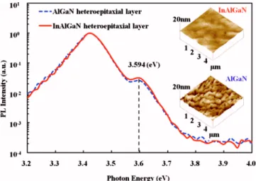
PL spectra of AlGaN and InAlGaN single heteroepitaxial layers grown on n-AlGaN/ud-GaN/sapphire substrate were obtained at a room temperature to investigate the band edge emission. Figure 1 shows that the PL emission energy of these two samples are very close 共about 3.594 eV兲 and the peak intensity of InAlGaN is slightly higher than AlGaN. The strong PL emission is attributed to the better crystal quality. Inset in Fig.1shows the surface morphology of the two AlGaN and InAlGaN single heteroepitaxial layers with the same thickness about 50 nm. The root-mean-square 共RMS兲 roughness measured by AFM is about 0.813 nm and 0.595 nm, respectively. The relatively high roughness of Al-GaN single heteroepitaxial layer can mainly be attributed to the low deposition temperature of 830 ° C necessary for the adjacent InGaN well.
Figure2共a兲shows the XRD 共-2兲 curves in the 共002兲 reflections of InGaN/AlGaN and InGaN/InAlGaN MQWs.
The results show that the locations of multiple
satellite peaks of InGaN/AlGaN and InGaN/InAlGaN MQWs are very close. This indicates that the thickness of barrier layer in these two samples is matched and it is quite consistent with the measured values of 11.7 nm from HRTEM images as shown in Figs.2共b兲and2共c兲. In addition to experimentally estimate the indium and aluminum compo-sition in the MQWs, we simulate the XRD共-2兲 curve by using dynamical diffraction theory. The In composition in the QWs was determined to be about 2.5%, where the thickness of the well was about 2.6 nm. The compositions of ternary and quaternary barriers were Al0.08Ga0.92N and In0.0085Al0.1112Ga0.8803N, respectively. Besides, the growth rates of well and barrier were estimated about 0.329 Å/s and 0.308 Å/s, respectively.
The optical properties of UV LED with ternary and qua-ternary barrier are shown in Fig. 3. Figure 3共a兲 shows the light output power-current-voltage共L-I-V兲 characteristics for the AlGaN and InAlGaN barrier UV LEDs. The forward voltage was 3.89 V and 3.98 V for InGaN/AlGaN and InGaN/InAlGaN MQWs UV LED at a forward current of
350 mA, respectively. A little high forward voltage of InAlGaN barrier LED can be attributed to the higher Al content compare to the AlGaN barrier, thus increase the se-ries resistance in the device. The light output power of InGaN-based UV LED with the InAlGaN barrier is higher by 25% and 55% than the AlGaN barrier at 350 mA and 1000 mA, respectively. Figure 3共b兲 shows the normalized effi-ciency curves of experimental 共open circles兲 and simulated 共solid lines兲 as a function of forward current for the two samples. For the InGaN/AlGaN UV LEDs, when the injec-tion current exceeds 1000 mA, the efficiency is reduced to 66% of its maximum value. In contrast, InGaN/InAlGaN UV LEDs exhibit only 13% efficiency droop when we increase the injection current to 1000 mA. The reduction in efficiency FIG. 1. 共Color online兲 Room-temperature PL spectra of AlGaN and
InAlGaN single heteroepitaxial layers. Inset in Fig.1shows surface mor-phology AFM over 5⫻5 m2of AlGaN共RMS: 0.813 nm兲 and InAlGaN
共RMS: 0.595 nm兲 layer with thickness about 50 nm. FIG. 2. 共Color online兲 共a兲 XRD 共-2兲 curves in the 共002兲 reflections of InGaN/AlGaN and InGaN/InAlGaN MQW. Cross-sectional TEM images of 共b兲 InGaN/AlGaN and 共c兲 InGaN/InAlGaN MQW. The diffraction condition is g = 0002.
FIG. 3.共Color online兲 共a兲 L-I-V curves of the LEDs with AlGaN 共dash兲 and InAlGaN共solid兲 barrier. 共b兲 Normalized efficiency curves of experimental 共open circles兲 and simulated 共solid lines兲. Inset in Fig.3共a兲shows the mesa-type UV chip.
211107-2 Tu et al. Appl. Phys. Lett. 98, 211107共2011兲
This article is copyrighted as indicated in the article. Reuse of AIP content is subject to the terms at: http://scitation.aip.org/termsconditions. Downloaded to IP: 140.113.38.11 On: Wed, 30 Apr 2014 09:06:45
droop is quite clear and the current at maximum efficiency shifts from 150 to 400 mA. Besides, the wavelength is nearly constant about 380 nm over the entire current range. The absence of temperature-induced redshift suggests that self-heating is substantially suppressed by using metal type pack-aging and pulsed mode operating.11 In order to investigate the physical origin of efficiency droop in these UV LEDs, we performed a simulation of the above structures by using the APSYS simulation software. Commonly accepted Shockley– Read–Hall recombination lifetime共about ⬃6 ns兲 and Auger recombination coefficient 共about ⬃10−30 cm6s−1兲 are used in the simulations. Other material parameters of the semicon-ductors used in the simulation can be found in Ref. 12. In addition, we can reduce the effect of spontaneous and piezoelectric polarizations because of lattice match condi-tion in barrier between AlGaN and InAlGaN. The total polarization fields in different combination of materials can be obtained through the calculation, and the results of In0.025Ga0.975N, Al0.08Ga0.92N, and In0.0085Al0.1112Ga0.8803N are the −0.0305 共C m−2兲, −0.0391 共C m−2兲, and −0.0398 共C m−2兲, respectively.13
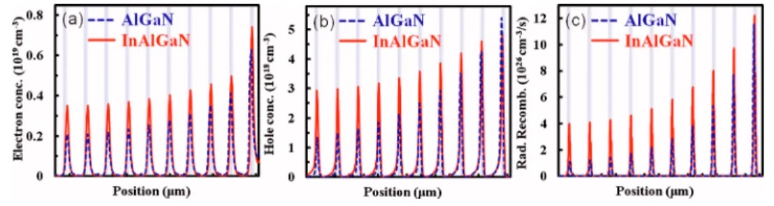
Besides, a different band-offset ratio from 6:4 to 7:3 is used in this simulation for introducing of indium in AlGaN. We can know that under the same energy band of barrier, the band-offset ratio from 6:4 to 7:3 will lead higher conduction-band and lower valence-band between well and barrier. This is useful for electron confinement and hole distribution in low indium content InGaN-based UV LEDs. However, another difficult problem is the inclusion of degenerate valence bands in mi-nority carrier hole mobility. Hence, to investigate the effi-ciency droop in these two samples, we assume that InGaN-based UV LED with InAlGaN barrier has relatively high carrier mobility. The values of mobility for electron and hole are assumed in the simulation,n-InGaN/AlGaN= 354 cm2/V s, n-InGaN/InAlGaN= 642 cm2/V s, p-InGaN/AlGaN= 2 cm2/V s, andp-InGaN/InAlGaN= 5 cm2/V s, respectively. Finally, the re-sults of the EQE droop simulation of both different structures are in good agreement with the experimental data as shown in Fig. 3共b兲. Finally, we have to check the actual carrier distribution in our simulation. Figure4shows the calculated carrier distribution in these UV LEDs structure under a high forward current density of 100 A/cm2共1000 mA兲 byAPSYS. When we apply the corresponding band-offset ratio and the carrier mobility in InGaN/InAlGaN MQWs, the electron and hole concentration increases in the QW by about 26% and 35%, respectively, and the distribution of carrier becomes more uniform than InGaN/AlGaN case. Under high current density, the carrier distribution of both electrons and holes determines how efficient the photon-emission process will be. As shown in Fig. 4, the peak-to-peak carrier ratio of InAlGaN barrier sample is reduced due to better carrier transportation and this is also more obvious in the hole dis-tribution. The direct consequence is the increasing radiative
recombination rate and thus the light output is expected to rise. On the other hand, in the traditional AlGaN barrier samples, the holes are locally concentrated in the first QW, which causes the unbalanced distribution between different types of carriers and thus leads to reduction in radiative re-combination rate. Comparing electrons and holes, holes suf-fer more as a result of this nonuniformity due to their large effective mass and low mobility. Thus, our InAlGaN design can reduce the carrier leakage and increase electron-hole pair radiative recombination simultaneously, especially for the distribution of holes.
In summary, we fabricated and compared the perfor-mance of LEDs of InGaN-based UV MQWs active region with ternary AlGaN and quaternary InAlGaN barrier layers. XRD and TEM measurements show the two barriers are con-sistent with the lattice and smooth morphology of quaternary InAlGaN layer can be observed in AFM. The electrolumines-cence results indicate that the light performance of the InGaN-based UV LEDs can be enhanced effectively when the conventional low temperature AlGaN barrier layers are replaced by the InAlGaN barrier layers. Furthermore, simu-lation results show that InGaN-based UV LEDs with quater-nary InAlGaN barrier exhibit 62% higher radiative recombi-nation rate and low efficiency droop of 13% at a high injection current. We attribute this improvement to increas-ing in carrier concentration and uniform redistribution of car-riers.
The authors are grateful to the National Science Council of the Republic of China, Taiwan, for financially supporting this research under Contract Nos. NSC 98-2221-E-009-003 and NSC 99-ET-E-009-001-ET.
1A. Sandhu,Nat. Photonics 1, 38共2007兲.
2Y. S. Tang, S. F. Hu, C. C. Lin, N. C. Bagkar, and R. S. Liu,Appl. Phys.
Lett. 90, 151108共2007兲.
3Y. C. Chiu, W. R. Liu, C. K. Chang, C. C. Liao, Y. T. Yeh, S. M. Jang, and
T. M. Chen,J. Mater. Chem. 20, 1755共2010兲.
4H. Hirayama,J. Appl. Phys. 97, 091101共2005兲.
5A. Knauer, H. Wenzel, T. Kolbe, S. Einfeldt, M. Weyers, M. Kneissl, and
G. Tränkle,Appl. Phys. Lett. 92, 191912共2008兲.
6M. F. Schubert, J. Xu, J. K. Kim, E. F. Schubert, M. H. Kim, S. Yoon, S.
M. Lee, C. Sone, T. Sakong, and Y. Park,Appl. Phys. Lett. 93, 041102 共2008兲.
7J. J. Wu, G. Y. Zhang, X. L. Liu, Q. S. Zhu, Z. G. Wang, Q. J. Jia, and L.
P. Guo,Nanotechnology 18, 015402共2007兲.
8S. H. Baek, J. O. Kim, M. K. Kwon, I. K. Park, S. I. Na, J. Y. Kim, B. J.
Kim, and S. J. Park,IEEE Photon. Technol. Lett. 18, 1276共2006兲.
9Q. Shan, Q. Dai, S. Chhajed, J. Cho, and E. F. Schubert,J. Appl. Phys.
108, 084504共2010兲.
10
APSYS by Crosslight Software Inc., Burnaby, Canada: http://
www.crosslight.com.
11Y. Yang, X. A. Cao, and C. Yan,IEEE Trans. Electron Devices 55, 1771
共2008兲.
12F. Bernardini, in Nitride Semiconductor Devices: Principles and Simula-tion, edited by J. Piprek共Wiley, New York, 2007兲, pp. 49–67.
13M. H. Kim, M. F. Schubert, Q. Dai, J. K. Kim, E. F. Schubert, J. Piprek,
and Y. Park,Appl. Phys. Lett. 91, 183507共2007兲.
FIG. 4.共Color online兲 Distribution of 共a兲 electron, 共b兲 hole concentrations, and 共c兲 radiative recombination rates concentrations of the LEDs with AlGaN and InAlGaN barrier under a high forward current density of 100 A/cm2.
211107-3 Tu et al. Appl. Phys. Lett. 98, 211107共2011兲
This article is copyrighted as indicated in the article. Reuse of AIP content is subject to the terms at: http://scitation.aip.org/termsconditions. Downloaded to IP: 140.113.38.11 On: Wed, 30 Apr 2014 09:06:45