Improved luminance intensity of InGaN–GaN light-emitting diode by roughening both
the p - Ga N surface and the undoped-GaN surface
Wei Chih Peng and Yew Chung Sermon Wu
Citation: Applied Physics Letters 89, 041116 (2006); doi: 10.1063/1.2236462
View online: http://dx.doi.org/10.1063/1.2236462
View Table of Contents: http://scitation.aip.org/content/aip/journal/apl/89/4?ver=pdfcov Published by the AIP Publishing
Articles you may be interested in
Light extraction enhancement of InGaN light-emitting diode by roughening both undoped micropillar-structure GaN and p - Ga N as well as employing an omnidirectional reflector
Appl. Phys. Lett. 93, 021125 (2008); 10.1063/1.2961008
Nitride-based light-emitting diodes with p - Al In Ga N surface layers prepared at various temperatures Appl. Phys. Lett. 89, 191112 (2006); 10.1063/1.2386914
Enhanced performance of an InGaN–GaN light-emitting diode by roughening the undoped-GaN surface and applying a mirror coating to the sapphire substrate
Appl. Phys. Lett. 88, 181117 (2006); 10.1063/1.2199613
High-efficiency 1.3 m InGaAs GaAs quantum-dot microcavity light-emitting diodes grown by metalorganic chemical vapor deposition
Appl. Phys. Lett. 86, 151118 (2005); 10.1063/1.1898440
In x Ga 1x N light emitting diodes on Si substrates fabricated by Pd–In metal bonding and laser lift-off Appl. Phys. Lett. 77, 2822 (2000); 10.1063/1.1319505
This article is copyrighted as indicated in the article. Reuse of AIP content is subject to the terms at: http://scitation.aip.org/termsconditions. Downloaded to IP: 140.113.38.11 On: Thu, 01 May 2014 01:53:57
Improved luminance intensity of InGaN–GaN light-emitting diode by
roughening both the p-GaN surface and the undoped-GaN surface
Wei Chih Peng and Yew Chung Sermon Wua兲
Department of Materials Science and Engineering, National Chiao Tung University, Hsinchu, Taiwan 300, Republic of China
共Received 28 October 2005; accepted 10 June 2006; published online 26 July 2006兲
The InGaN–GaN epitaxial films were grown by low-pressure metal-organic chemical vapor deposition on a sapphire substrate, and then the light-emitting diode共LED兲 with double roughened 共p-GaN and undoped-GaN兲 surfaces was fabricated by surface-roughening, wafer-bonding, and laser lift-off technologies. It was found that the front side luminance intensity of double roughened LED was 2.77 times higher than that of the conventional LED at an injection current of 20 mA. The backside luminance intensity was 2.37 times higher than that of the conventional LED. This is because the double roughened surfaces can provide photons multiple chances to escape from the LED surface, and redirect photons, which were originally emitted out of the escape cone, back into the escape cone. © 2006 American Institute of Physics.关DOI:10.1063/1.2236462兴
The epitaxial growth techniques have significantly im-proved the brightness and efficiency of light-emitting diode 共LED兲.1
Some techniques have been employed to reduce the dislocation density through epitaxial lateral overgrowth 共ELO兲,2,3
lateral epitaxial patterned sapphire 共LEPS兲,4,5 and SiNx interlayer6 using a metal-organic vapor-phase epitaxy. These improvements have enabled LED to be widely applied to mobile phones, full-color displays, and lighting.7The LED operating in the wavelength region ranging from blue to green light has been employed by the InGaN–GaN alloy sys-tem grown on sapphire substrates. However, the efficiency of conventional LED is limited by their inability to emit all of the light that is generated from the active layer. According to Snell’s law, light traveling from a GaN surface having a high index of refraction 共n=2.5兲 to an air with a low index of refraction共n=1.0兲 that is only within a critical angle of 23° will cross the air. The light reaching the surface beyond the critical angle will not cross the air but will experience total internal reflection that continues to be reflected within the LED until it is absorbed. One method of reducing the per-centage of total internal reflection light is to create light scat-tering centers in the form of random texturing on the LED’s surface.8 However, the thickness of the top layer
p-GaN cladding is very thin. Consequently, it is not easy to
control the dry etching depth and plasma damage to the
p-GaN during the dry etching process. Some methods have
been used to improve the light extraction efficiency by roughening the top surface9–13 or the mesa sidewall14 of LED. It could also utilize wafer-bonding technology to trans-fer n-side-up GaN-based LED on Si substrates with a hex-agonal “conelike” surface on n-GaN.15All these studies de-scribed above were focused on a single roughened top surface of nitride-based LED. In this study, LED with double roughened surfaces was proposed. It was fabricated using surface-roughening, wafer-bonding, and laser lift-off technologies.
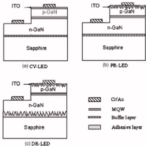
Three kinds of LED were investigated in this study. Their specifications and structures are schematically
illus-trated in Fig. 1. Samples designated as “CV-LED” were con-ventional LEDs without any surface-roughening treatment. Samples designated as “PR-LED” were LEDs with a
p-GaN roughened surface, while “DR-LED” were LEDs
with double roughened共p-GaN and undoped-GaN兲 surfaces. The basic processes of these LEDs were almost the same. The InGaN–GaN films were grown by low-pressure metal-organic chemical vapor deposition共MOCVD兲 on a sapphire substrate. The LED structures and growth temperature in-cluded a p-type Mg-doped GaN at 950 ° C, an InGaN–GaN multiquantum well 共MQW兲 with six pairs of InGaN 共3 nm兲/GaN 共9 nm兲 at 800 °C, a 2-m-thick n-type Si-doped GaN at 1050 ° C, a 2-m-thick undoped-GaN layer film at 1050 ° C, and a buffer layer at 550 ° C on the sapphire substrate. The major difference was that the thickness of the
p-type GaN of CV-LED was 0.2m, which was thinner than that of PR-LED and DR-LED samples, 0.5m. This extra length of the p-type GaN layer was employed to create the roughened p-type GaN surface by lowering the epitaxy growth temperature.13
a兲Author to whom correspondence should be addressed; FAX:
886-3-572-4727; electronic mail: [email protected]
FIG. 1. Schematic diagrams of 共a兲 CV-LED 共without any surface-roughening treatment兲, 共b兲 PR-LED 共with roughened p-GaN surface兲, and 共c兲 DR-LED 共with double roughened surfaces兲.
APPLIED PHYSICS LETTERS 89, 041116共2006兲
0003-6951/2006/89共4兲/041116/3/$23.00 89, 041116-1 © 2006 American Institute of Physics This article is copyrighted as indicated in the article. Reuse of AIP content is subject to the terms at: http://scitation.aip.org/termsconditions. Downloaded to IP:
For the CV-LED and PR-LED, the device of 300 ⫻300m2 dimension was defined by inductively coupled plasma 共ICP兲 to remove Mg-doped GaN and MQW until Si-doped GaN was exposed. Then, the indium tin oxide 共ITO兲 layer was deposited on the p-GaN layer 共
⬃4 ⍀ cm兲 to form a p-side contact layer and a current spreading layer. Finally, Cr/ Au was deposited onto the ITO layer and n-GaN layer as the electrodes. The structures were shown in Figs. 1共a兲 and 1共b兲, respectively.
As for the fabrication of DR-LED devices, PR-LED wa-fer was bonded to a host substrate covered with adhesive layer. The optical transparency of the adhesive layer was exceeding than 90% across the visible spectrum. It was then annealed at 200 ° C for 60 min. After bonding, the sapphire substrate was removed by laser lift-off with a frequency-tripled neodymium-doped yttrium aluminum garnet laser at 355 nm.16 The roughened undoped-GaN surface was ob-tained by treatment with 60 ° C KOH solution for 1 min. The wafer was then bonded to sapphire substrate with an adhe-sive layer. Finally, the host substrate was removed. The structure of DR-LED was shown in Fig. 1共c兲.
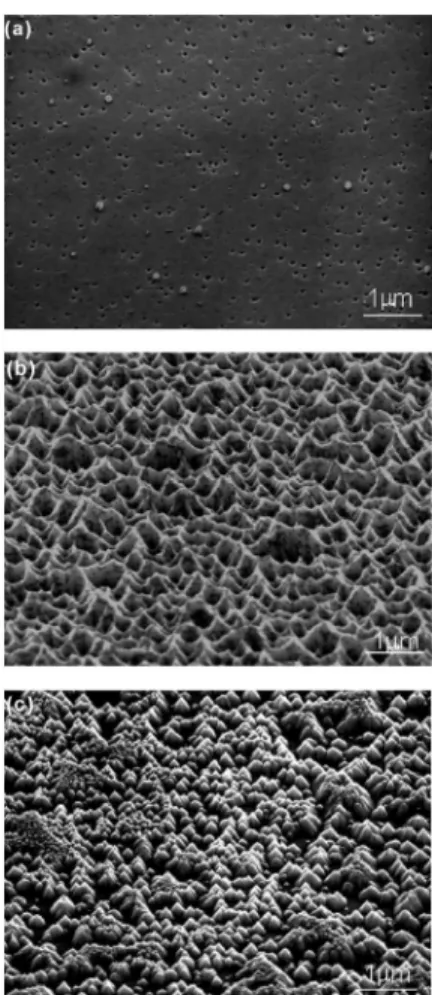
Figure 2 shows the morphologies of LED surfaces. Clearly, the surface of CV-LED is much smoother than that of PR-LED. Their surfaces were measured using atomic force microscopy共AFM兲. The root mean square 共rms兲 rough-ness of p-GaN surface without any treatment is only 11.8 nm, while that of roughened p-type GaN surface is 71.6 nm. As for the surface of the roughened undoped-GaN layers the surface was full with three-dimensional islands.
The height and size of the GaN islands were 300– 700 nm and 0.1– 0.4m, respectively. The rms roughness of this undoped-GaN surface was 91.9 nm.
The I-V characteristics of the PR-LED and DR-LED ex-hibited normal p-n diode behaviors with forward voltages about 3.3 V at 20 mA, which was similar to that of CV-LED 共3.2 V at 20 mA兲. This similarity indicated that the surface-roughening process, wafer-bonding process, and laser lift-off process did not degrade the performance of DR-LED. To further investigate the influence of roughened GaN surfaces on light-output performance of LED chips, the luminance intensities of unpackaged LED were measured from both the front side 共top side through the transparent ITO layer兲 and backside 共substrate side through the sapphire/transparent glue/glass兲 of the device. The light intensities as a function of injected forward current are shown in Figs. 3共a兲 and 3共b兲, respectively. It is obvious that roughened surfaces of LED did enhance the luminance intensities.
Compared with that of the CV-LED chip, the light inten-sity of the PR-LED chip with a roughened p-GaN surface was increased by 60% for the front side and by 56% for the backside at an injection current of 20 mA. The reason why the greater increase in light intensity measured from the front side than from the backside is because the microroughened top surface for the front side was thought to give the photons multiple chances to escape from the LED to the surrounding air. These results are similar to the conclusions drawn by Hu
et al.4 in their studies on microroughening of the p-GaN surface. They measured the light-output powers of unpack-aged LED chips from both front side and backside of the device. They also found that the light-output powers were increased on both sides, and the increase from the front side was also higher than that from the backside. Compared with that of the conventional LED chip, the light-output power for the LED chip with a microroughened top surface was in-creased by 52.4% for the front side and by 30% for the backside, respectively. Moreover, our increase in light inten-sities from both sides was higher than those obtained by Hu
et al. This is because the rms roughness of our roughened p-type GaN surface is 71.6 nm, which is higher than that of
the samples of Hu et al., 6 nm.
As for the luminance intensity of our DR-LED, the light intensities from both sides were greatly enhanced. The front side luminance intensity was 133 mcd, which was 2.77 times FIG. 2. Scanning electron micrographs of共a兲 p-GaN surface without any
surface-roughening treatment,共b兲 roughened p-GaN surface, and 共c兲 rough-ened undoped-GaN surface.
FIG. 3. Luminance intensity of three LED chips vs the forward injection current. 共a兲 Intensity measured from the front side 共topside through the transparent metal layer兲 of the LED chip. 共b兲 Intensity measured from back-side substrate back-side共through the sapphire/transparent glue/glass兲 of the LED chip.
041116-2 W. C. Peng and Y. C. S. Wu Appl. Phys. Lett. 89, 041116共2006兲
This article is copyrighted as indicated in the article. Reuse of AIP content is subject to the terms at: http://scitation.aip.org/termsconditions. Downloaded to IP: 140.113.38.11 On: Thu, 01 May 2014 01:53:57
higher than that of the CV-LED, and 1.73 times higher than that of the PR-LED. As for the backside luminance intensity, it was 178 mcd, which was 2.37 times higher than that of the CV-LED and 1.52 times higher than that of the PR-LED. Clearly, this tremendous enhancement was caused by the roughened p-GaN surface and the roughened undoped-GaN surface. The increase in light intensity measured from the front side was still higher than that from the backside, even though the rms roughness of the roughened undoped-GaN surface 共91.9 nm兲 was much higher than that of the p-type GaN surface共71.6 nm兲. This is because during bonding pro-cess, we might create interfacial defects at two bonded inter-faces 共GaN/adhesive layer and adhesive layer/sapphire兲. These defects have a negative effect on optical properties, and it is suggested that this might be the reason why the increase in backside luminance intensity was not as high as we expected. In addition, Fresnel losses resulting from the GaN 共n⬃2.5兲/adhesive layer 共n⬃1.5兲 and adhesive layer 共n⬃1.5兲/sapphire 共n⬃1.7兲 interfaces might also have a negative effect on the backside luminance intensity.
The light extraction efficiency in the GaN-based LED is limited mainly due to the difficulty for light to escape from high refractive index semiconductors. The key to enhance the escape probability is to give the photons multiple oppor-tunities to find the escape cone.3As shown in Fig. 4, rough-ened surfaces not only can provide photons multiple chances to escape from the LED surface, but also redirect photons, which were originally emitted out of the escape cone, back into the escape cone. Figure 4共a兲 shows the possible photon paths for CV-LED without any roughened surface. For a
PR-LED, the angular randomization of photons can be achieved by surface scattering from the roughened p-GaN surface, as shown in Fig. 4共b兲. Thus, the roughened surface structure can provide photons multiple chances to escape from the LED, and redirect photons back into the escape cone. A DR-LED device has two roughened surfaces, as shown in Fig. 4共c兲. Compared to the PR-LED, the extraroughened undoped-GaN layer can greatly increase the escape probability of photons, resulting in an increase in the luminance intensity of LED, as shown in Fig. 3.
In summary, DR-LED with double roughened 共p-GaN and undoped-GaN兲 surfaces was investigated in this study. It was fabricated by surface-roughening, wafer-bonding, and laser lift-off technologies. It was found that surface-roughening, wafer-bonding, and laser lift-off processes did not degrade the performance of DR-LED. At an injection current of 20 mA, the front side luminance intensity of double roughened LED was 133 mcd, which was 2.77 times higher than that of the conventional LED, and the backside luminance intensity was 178 mcd, which was 2.37 times higher than that of the conventional LED. This is because the double roughened surfaces not only can provide photons multiple chances to escape from the LED surface, but also redirect photons, which were originally emitted out of the escape cone, back into the escape cone.
This project was funded by Epistar Corporation and the National Science Council 共NSC兲 of the Republic of China under Grant No. 94-2216-E009-015.
1S. Nakamura, S. Senoh, N. Iwasa, and S. Nagahama, Jpn. J. Appl. Phys.,
Part 2 34, L797共1995兲.
2I. Kidoguchi, A. lshibashi, G. Sugahara, and Y. Ban, Appl. Phys. Lett. 76,
3768共2000兲.
3T. Mukai, K. Takekawa, and S. Nakamura, Jpn. J. Appl. Phys., Part 2 37,
L839共1998兲.
4K. Tadatomo, H. Okagawa, T. Tsunekawa, T. Jyouichi, Y. Imada, M. Kato,
H. Kudo, and T. Taguchi, Phys. Status Solidi A 188, 121共2001兲.
5S. J. Chang, Y. C. Lin, Y. K. Su, C. S. Chang, T. C. Wen, S. C. Shei, J. C.
Ke, C. W. Kuo, S. C. Chen, and C. H. Liu, Solid-State Electron. 47, 1539 共2003兲.
6R. C. Tu, C. C. Chuo, S. M. Pan, Y. M. Fan, C. E. Tsai, T. C. Wang, C. J.
Tun, G. C. Chi, B. C. Lee, and C. P. Lee, Appl. Phys. Lett. 83, 3608 共2003兲.
7H. X. Jiang, S. X. Jin, J. Li, J. Shakya, and J. Y. Lin, Appl. Phys. Lett. 78,
1303共2001兲.
8I. Schnitzer, E. Yablonovitch, C. Caneau, T. J. Gmitter, and A. Scherer,
Appl. Phys. Lett. 63, 2174共1993兲.
9R. Windisch, B. Dutta, M. Kuijk, A. Knobloch, S. Meinlschmidt, S.
Schoberth, P. Kiesel, G. Borghs, G. H. Dohler, and P. Heremans, IEEE Trans. Electron Devices 47, 1492共2000兲.
10Chul Huh, Kug-Seung Lee, Eun-Jeong Kang, and Seong-Ju Park, J. Appl.
Phys. 93, 9383共2003兲.
11Y. P. Hsu, S. J. Chang, Y. K. Su, S. C. Chen, J. M. Tsai, W. C. Lai, C. H.
Kuo, and C. S. Chang, IEEE Photonics Technol. Lett. 17, 1620共2005兲.
12C. M. Tsai, J. K. Sheu, W. C. Lai, Y. P. Hsu, P. T. Wang, C. T. Kuo, C. W.
Kuo, S. J. Chang, and Y. K. Su, IEEE Electron Device Lett. 26, 464 共2005兲.
13C. H. Liu, R. W. Chuang, S. J. Changb, Y. K. Su, L. W. Wu, and C. C. Lin,
Mater. Sci. Eng., B 112, 10共2004兲.
14C. F. Lin, Z. H. Yang, J. H. Zheng, and J. H. Dai, IEEE Photonics Technol.
Lett. 17, 2038共2005兲.
15T. Fujii, Y. Gao, R. Sharma, E. L. Hu, S. P. DenBaars, and S. Nakamura,
Appl. Phys. Lett. 84, 855共2004兲.
16M. K. Kelly, O. Ambacher, R. Dimitrov, R. Handschuh, and M.
Stutzmann, Phys. Status Solidi A 159, R3共1997兲. FIG. 4. Possible photon paths inside the structures of the共a兲 CV-LED, 共b兲
PR-LED, and共c兲 DR-LED.
041116-3 W. C. Peng and Y. C. S. Wu Appl. Phys. Lett. 89, 041116共2006兲
This article is copyrighted as indicated in the article. Reuse of AIP content is subject to the terms at: http://scitation.aip.org/termsconditions. Downloaded to IP: 140.113.38.11 On: Thu, 01 May 2014 01:53:57