This content has been downloaded from IOPscience. Please scroll down to see the full text.
Download details:
IP Address: 140.113.38.11
This content was downloaded on 26/04/2014 at 05:30
Please note that terms and conditions apply.
Fabrication and characteristics of thin-film InGaN–GaN light-emitting diodes with TiO2/SiO2
omnidirectional reflectors
View the table of contents for this issue, or go to the journal homepage for more 2007 Semicond. Sci. Technol. 22 831
(http://iopscience.iop.org/0268-1242/22/7/029)
Semicond. Sci. Technol. 22 (2007) 831–835 doi:10.1088/0268-1242/22/7/029
Fabrication and characteristics of
thin-film InGaN–GaN light-emitting
diodes with TiO
2
/SiO
2
omnidirectional
reflectors
C H Chiu
1, H C Kuo
1, C E Lee
1, C H Lin
2, P C Cheng
1,
H W Huang
1, T C Lu
1, S C Wang
1and K M Leung
21Department of Photonics, National Chiao Tung University, Hsinchu 30050, Taiwan,
Republic of China
2Department of Computer and Information Science, Polytechnic University,
Six Metrotech Center, Brooklyn, NY 11201, USA E-mail:[email protected]
Received 29 November 2006, in final form 26 April 2007 Published 21 June 2007
Online atstacks.iop.org/SST/22/831
Abstract
In this paper, a novel GaN-based thin-film vertical injection light-emitting diode (LED) structure with a TiO2and SiO2omnidirectional reflector
(ODR) and an n-GaN rough surface is designed and fabricated. The designed ODR, consisting of alternating TiO2and SiO2, layers possesses a
complete photonic band gap within the blue region of interest. The arrays of the conducting channels are integrated into the TiO2/SiO2ODR structure for
vertically spreading the current. Assisted by the laser lift-off and photo-enhanced chemically etched surface roughening process, the light output power and the external quantum efficiency of our thin-film LED with a TiO2/SiO2ODR (at a driving current of 350 mA and with chip size of
1 mm× 1 mm) reached 330 mW and 26.7%, increased by 18% and 16%, respectively, compared with the results from the thin-film LED with an Al mirror. By examining the radiation patterns of the LEDs, the optical output power mainly increased within the 120 deg cone due to the higher
reflectance of the TiO2/SiO2ODR within the blue regime.
(Some figures in this article are in colour only in the electronic version)
Introduction
Direct wide-bandgap gallium nitride (GaN) and other III– nitride-based semiconductors have attracted much attention for potential applications such as outdoor displays, exterior automotive lightings, backlight for various handheld devices, printers, liquid crystal display TVs and rear projection TVs [1, 2]. Recently, the high brightness GaN-based light-emitting diode (LED) has shown good performance for those applications. However, further improvement on the optical output power and light extraction efficiency is necessary for the next generation applications such as projectors, automobile headlight and general lightings. The thin-film LED structure shows great enhancement of the light extraction efficiency
due to combining the processes of laser lift-off (LLO) to remove the sapphire substrate by an excimer laser and photo-electrochemical (PEC) etching to rough the exposed n-GaN surface. An N-metal electrode of the thin-film LED is deposited on the roughened n-GaN surface and the cathode connection is performed by means of a wire bond. The p-GaN surface of the LED in such a vertical structure is metalized and bonded to another semiconductor substrate such as Si wafers to serve as an anode. Such a structure shall be a good candidate to satisfy the next generation requirement and several groups have demonstrated excellent performance on light output power with high injection current [3–6].
The vertical structure LED with better extraction efficiency and higher light output is mainly because of the
C H Chiu et al
embedded reflector. The reflector on the bottom can reflect the downward emitting light upward towards the emitting substrate effectively to contribute to the useable light and enhance the light extraction efficiency. Metallic materials with high refractivity such as Ag or Al have been used for this purpose [7]. The metallic mirror indeed shows good reflectivity for arbitrary angles and polarizations but they are somewhat lossy in the visible regime [8]. In addition, the metallic mirror also has reliability problems at the interface with a semiconductor due to degradation or electromigration. In particular, a recent work indicated that the absorption by metallic mirrors becomes more severe as the thickness of the device is reduced [9]. As a result, dielectric mirrors, such as distributed Bragg reflectors (DBRs) [10] have been widely used to solve those problems. Compared with metallic counterparts, DBRs have many advantages, such as very low optical loss, high reflectance and high mechanical robustness [11]. However, only light of a given polarization impinging near the normal direction to the DBR structure can be effectively reflected. Total reflection of light with arbitrary polarization and incidence angle onto a periodic structure can be realized with the existence of a complete photonic band gap (CPBG) at the wavelengths of interest [12]. A one-dimensional periodic dielectric structure possessing this characteristic is known as an omnidirectional one-dimensional photonic crystal (1D PhC). By selecting appropriate thickness of the dielectric layers, there is no allowed photon propagation state for wavelengths within the CPBG. Such an omnidirectional reflector (ODR) made from the designed 1D PhC can totally reflect the light with wavelengths within the CPBG at any incidence angle and polarization. Therefore, compared with DBRs, a substantially higher reflectance can be achieved by ODRs. In our previous work, we have demonstrated enhancement in the extracted light intensity for a GaN-based LED with p-side up and flip-chip configuration incorporated with an ODR composed of alternate layers of TiO2 and SiO2 [13, 14]. An ultra-high
brightness thin-film vertical-injection LED with the ODR composed of TiO2 and SiO2 and a PEC roughened surface
is demonstrated and achieved in this paper.
Device fabrication
The InGaN/GaN vertical-injection LED samples were grown by metal organic chemical vapour deposition with a rotation disc reactor (Encore) on a c-axis sapphire (0 0 0 1) substrate at a growth pressure of 200 mbar. The prepared InGaN/GaN vertical-injection LED wafer consists of a 50 nm thick GaN nucleation layer grown at 550 ◦C, a 3 µm thick Si-doped n-GaN buffer layer grown at 1050 ◦C, an unintentionally doped InGaN/GaN multiple quantum well (MQW) active region grown at 770◦C, a 50 nm thick Mg-doped p-AlGaN electron blocking layer grown at 1050◦C, a 0.15 µm thick Mg-doped p-GaN contact layer grown at 1050◦C and a Si-doped n-In0.23Ga0.77N/GaN short period super lattice (SPS)
structure. The MQW active region consists of five periods of 3 nm/7 nm thick In0.21Ga0.79N/GaN quantum well layers
and barrier layers. By performing a split-wafer experiment, the original InGaN/GaN MQW LED wafers with a backside polished sapphire substrate were cleaved to the size of
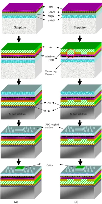
ODR Al mirror
Au
Si host substrate Si host substrate
Au Ti PEC roughed surface Conducting Channels Cr/Au Sapphire Sapphire n-GaN MQW p-GaN ITO (a) (b)
Figure 1. Fabrication flowchart of n-side surface roughness
vertical-injection LED structures (a) with the Al mirror, and (b) with the ODR composed of TiO2/SiO2.
1.5 × 1.5 cm2. These LED samples were separated into
two sets for different process procedures, with Al mirrors and ODRs.
As shown in figure1(a), the first set of samples was the InGaN/GaN vertical-injection LED with an Al mirror. A transparent conducting layer composed of indium-tin-oxide (ITO) with a thickness of 300 nm is first deposited onto the p-GaN surface by electron beam (E-beam) evaporation. The ITO layer had a high transparency (>95% at 460 nm) and high electrical conductivity for current spreading. For the vertical-injection LED structure with an Al mirror, the sample was prepared by depositing the Al layer with a thickness of 1 µm by E-beam evaporation on the ITO surface. Then an Au layer with a thickness of 1.4 µm was deposited onto the surface of the forming Al layer for the purpose of bonding with the silicon 832
Figure 2. Photonic band diagram of a 1D PC composed of TiO2and
SiO2multi-layers. Refractive indices and layer thickness are
assumed to be 2.52, 56 nm for TiO2and 1.48, 77 nm for SiO2,
respectively. The red and white regions represent the allowed and forbidden photon states. The lines in the diagonal directions identify the edges of the light cone. The region with red area of the CPBG represents an omnidirectional reflection region.
wafer. As shown in figure1(b), the second set of samples was the vertical-injection LED structure with an ODR. Conducting channels were integrated inside the ODR to contact with ITO for vertical current spreading. An array of lift-off resist (LOR) posts with diameter 50 µm and height 7 µm was first defined by a standard photolithographic process on the ITO surface. Second, the designed ODR of the TiO2/SiO2multilayer stake
was directly deposited onto the defined post array by E-beam evaporation. Third, those posts were moved away by a lift-off procedure. Finally, a thick layer of Cr/Pt/Au of 1.4 µm was deposited by E-beam evaporation and the formed holes inside the ODR were filled with Cr/Pt/Au to serve as conducing channels or p-GaN metal contacts. We also deposited a layer of Au with a thickness of 1.4 µm on the ODR surface for proceeding the wafer bonding process.
LED samples with Al mirrors and ODRs were then bonded onto a p-type conducting Si substrate (with the bonding metal of 0.7 µm Ti and 1.4 µm Au) by a commercial SUSS SB6e wafer bonder with a bonding temperature of 340 ◦C and a bonding pressure of 17 kg cm−2for 140 min. After that, the wafer-bonded samples underwent the LLO process. A KrF excimer laser with a beam size of 1.2 mm× 1.2 mm at a wavelength of 248 nm with a pulse width of 25 ns and the incident laser fluence of 300 mJ cm−2 was used to remove the sapphire substrate [15]. In order to thin out the revealed n-GaN, the whole sapphire-removed samples were etched by inductively coupled the plasma reactive ion etching (ICP-RIE) system (SAMCO ICP-RIE 101iPH) and the associated mesas were etched further down to the ODR interface for isolating the individual chip. To further increase the light extraction efficiency, the n-GaN surfaces of the samples were roughened through PEC etching by using an UV lamp and the dilute aqueous solution of KOH [16]. Finally, a patterned Cr/Au electrode was deposited onto the n-GaN surface as an n-type contact layer.
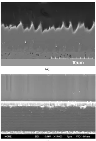
10 um 10 um
(a)
(b)
Figure 3. (a) SEM images of the roughened surface by PEC
process. (b) Cross-sectional SEM images of the vertical-injection LED with TiO2/SiO2multi-layers.
Result and discussion
Figure2shows the band structure of the ODR composed of TiO2and SiO2with different dielectric layer thicknesses using
the transmission-line method [17]. The reflective indices of TiO2and SiO2are 2.52 and 1.48, respectively. We found that
the optimal CPBG is at frequencies between 0.282 c/a and 0.304 c/a (the red region shown in figure3), and at thicknesses of 0.421a and 0.579a, respectively for the TiO2and SiO2layers
where c and a are the speed of light and the lattice constant. In this paper, we chose the lattice constant a= 133 nm to give a CPBG centred at 455 nm. Thus the TiO2and SiO2layers have
a thickness of 56 nm and 77 nm respectively and the ODR has a CPBG between 437 nm and 472 nm. When the desired ODR composed of TiO2and SiO2is fabricated on the GaN
LED with a peak emitting wavelength of 455 nm, it will show very a high reflectance for the wavelength falling within the emitting spectrum of the LED.
Figure 3(a) shows the SEM images of the roughened surface after the PEC roughening process on the n-GaN material. The roughened surface can enhance the external quantum efficiency since the total internal reflection was destroyed by the roughened surface. Figure3(b) shows the cross-sectional SEM image of the ODR incorporated in our thin-film InGaN/GaN LED. The designed ODR composes of 14 pairs of TiO2/SiO2layers evaporated onto the ITO layer by
an E-beam evaporator.
Figure 4(a) shows the forward I–V curves of the thin-film vertical-injection LED with the TiO2/SiO2 ODR and
C H Chiu et al 0 200 400 600 800 1000 1200 1400 0 200 400 600 800 1000 1200 External Quantum Effici ency (% )
Vertical LED with Al reflector Vertical LED with 1D PC
Output Power ( m W) Current (mA) 0 10 20 30 40 50 60 400 450 500 550 0 2 4 6 8 10 12 14 In ten s ity (a.u .) Wavelength (nm) 0 200 400 600 800 1000 1200 1400 0 1 2 3 4 5 V o ltag e (V ) Current (mA) VLED with 1D PC VLED with Al reflector
(a)
(b)
Figure 4. (a) Current–voltage (I–V) and (b) intensity–current (L–I)
and external quantum efficiency versus forward dc current of the LEDs with a TiO2/SiO2ODR and with an Al reflector. The inset
shows the room temperature EL spectra at a driving current of 350 mA.
with an Al mirror. The forward voltage of LED with a TiO2/SiO2 ODR is slightly higher than that of LED with
an Al mirror. The measured forward voltages under an injection current of 350 mA at room temperature for the LEDs with a TiO2/SiO2 ODR and with an Al mirror are
approximately 3.52 V and 3.46 V, respectively. The slightly higher forward voltage of the LED with a TiO2/SiO2ODR
than that with an Al mirror can be attributed to additional thermal processes during the ODR deposition. We believe that the ITO/SPS layer’s interfacial mixing can result in a higher specific contact resistance and hence can raise the LED operation voltage. In addition, the current spreading via the conducting channels inside the ODR can cause the forward voltage slightly higher. Figure 4(b) shows light output power and external quantum efficiency versus applying forward dc current for the LEDs with a TiO2/SiO2 ODR
and with an Al mirror. At an injection current of 350 mA, the light output power of the LED with a TiO2/SiO2ODR
and the LED with an Al mirror are approximately 330 mW and 279 mW, respectively. The LED with a TiO2/SiO2ODR
increased the output power by a factor of 1.18, indicating that LED with a TiO2/SiO2ODR has higher reflectance and better
light extraction efficiency than that with an Al mirror. The current-dependent external quantum efficiency is similar to the case of the output power versus the forward dc current. The external quantum efficiency of the LED with a TiO2/SiO2
0 15 30 45 60 75 90 105 120 135 150 165 180
Vertical LED with Al + roughness Vertical LED with TiO
2/SiO2 ODR + roughness
Figure 5. Comparison of the radiation patterns in air between LEDs
with a TiO2/SiO2ODR and with an Al mirror, respectively.
0 100 200 300 400 500 600 700 800 900 1000 0 50 100 150 200 250 300 350 400 450 500 Output Power (mW) Lifetime (hours)
Figure 6. The life test results of the LEDs with TiO2/SiO2ODRs
under the condition of a 350 mA driving current and 55◦C ambient temperature.
ODR is 1.16 times higher than the LED with an Al mirror under all our measurement conditions. According to figure 4(b), at a driving current of 350 mA, the external quantum efficiencies for the LED with a TiO2/SiO2 ODR and with
an Al mirror are 26.7% and 23.0%, respectively. The inset of figure4(b) shows the typical room temperature EL spectra of InGaN-based LEDs with a TiO2/SiO2ODR and an Al mirror
at a driving current of 350 mA. We can see that the InGaN-based MQW emission peaks of those two devices are both located at 455 nm. However, the EL intensity of the LED with a TiO2/SiO2ODR is larger than that of the LED with an
Al mirror since the LED with an ODR has a higher external quantum efficiency.
We also measured the light output radiation patterns of the thin-film InGaN/GaN LED with an ODR and the LED with an Al mirror at a driving current of 350 mA (figure5). It can be seen that the LED with the TiO2/SiO2ODR shows
a higher optical power within 120 deg cone than that of the LED with an Al mirror. This enhancement is attributed to the higher reflectance of our ODR within the blue regime when compared with that of an Al mirror.
During life test, nine thin-film InGaN/GaN LEDs with ODRs and PEC roughness were encapsulated and mount on a 834
heat sink. All LEDs were driven by 350 mA current injection at a 55◦C ambient temperature. As shown in figure6, after 1000 h, good ageing behaviour was observed except for a small decrease of the output power in the initial few hours. It also shows that the output power of the thin-film InGaN/GaN LED with ODR and PEC roughness only decreased by 7–11% and indicates that the structure is a reliable and promising method for device production.
Conclusion
In summary, the thin-film InGaN/GaN vertical-injection LED with a TiO2/SiO2ODR and n-GaN PEC roughness process is
designed and fabricated. At a driving current of 350 mA and with a chip size of 1 mm× 1 mm, the light output power and the external quantum efficiency of the LED with a TiO2/SiO2
ODR reache 330 mW and 26.7%, increased by 18% and 16%, respectively, compared with the results from the LED with an Al mirror. The radiation pattern of the LED with a TiO2/SiO2
ODR shows a higher optical power within 120 deg cone due to the higher reflectance of the designed ODR within the blue regime than those LEDs of Al mirrors. The life time test indicates that the structure is reliable and promising for device production.
Acknowledgments
This work is supported by the National Science Council of Republic of China (ROC) in Taiwan under contract NSC 95-2221-E-009-282 and NSC 95-2752-E-229-007-PAE.
References
[1] Nakamura S, Mukai T and Senoh M 1994 Appl. Phys. Lett. 64 1687–9
[2] Stringfellow G B and Craford George M 1997 (Boston, MA: Academic)
[3] Wierer J J et al 2001 Appl. Phys. Lett.78 3379–81
[4] Gao Y, Fujii T, Sharma R, Fujito K, Denbaars S P,
Nakamura S and Hu E L 2004 Japan. J. Appl. Phys.43 637
[5] Song J, Lee D S, Kwak J S, Nam O H, Park Y and Seong T Y 2004 IEEE Photon. Technol. Lett. 16 1450–2
[6] Chang S J, Chang C S, Su Y K, Lee C T, Chen W S, Shen C F, Hsu Y P, Shei S C and Lo H M 2005 IEEE Trans. Adv. Packag. 28 273–7
[7] Kim J K, Gessmann Th, Luo H and Schubert E F 2004 Appl. Phys. Lett. 84 4508–10
[8] Fink Y, Winn J N, Fan S, Chen C, Michel J, Joannopoulos J D and Thomas E L 1998 Science282 1679–82
[9] David A, Fujii T, Moran B, Nakamura S, DenBaars S P, Weisbush C and Benisty H 2006 Appl. Phys. Lett.
88 133514
[10] Zhao Y S, Hibbard D L, Lee H P, Ma K, So W and Liu H 2003 J. Electron. Mater.32 1523
[11] Xi J Q, Ojha M, Plawsky J L, Gill W N, Kim J K and Schubert E F 2005 Appl. Phys. Lett.87 031111
[12] Joannopoulos J D, Meade R and Winn J N 1995 (Princeton, NJ: Princeton University Press)
[13] Lin C H, Tsai J Y, Kao C C, Kuo H C, Yu C C, Lo J R and Leung K M 2006 Japan J. Appl. Phys.45 1591
[14] Lin C H, Lai C F, Ko T S, Huang H W, Kuo H C, Hung Y Y, Leung K M, Yu C C, Tsai R J, Lee C K, Lu T C and Wang S C 2006 IEEE Photon. Technol. Lett. 18 2050–2 [15] Chu C F, Yu C C, Cheng H C, Lin C F and Wang S C 2003
Japan J. Appl. Phys.42 L147
[16] Lin C F, Zheng J H, Yang Z J, Dai J J, Lin D Y, Chang C Y, Lai Z X and Hong C S 2006 Appl. Phys. Lett.88 083121
[17] Lin C H, Leung K M and Tamir T 2002 J. Opt. Soc. Am. A