Growth of single-crystalline Ru O 2 nanowires with one- and two-nanocontact electrical
characterizations
Yee-Lang Liu, Zong-Yi Wu, Kuei-Jiun Lin, Jr-Jeng Huang, Fu-Rong Chen, Ji-Jung Kai, Yong-Han Lin, Wen-Bin Jian, and Juhn-Jong Lin
Citation: Applied Physics Letters 90, 013105 (2007); doi: 10.1063/1.2428669 View online: http://dx.doi.org/10.1063/1.2428669
View Table of Contents: http://scitation.aip.org/content/aip/journal/apl/90/1?ver=pdfcov Published by the AIP Publishing
Articles you may be interested in
Adaptive wiring for 20 nm scale epitaxial silicon Ohmic contacts to silicon nanowires J. Vac. Sci. Technol. B 25, 2572 (2007); 10.1116/1.2798738
Effects of channel-length scaling on In 2 O 3 nanowire field effect transistors studied by conducting atomic force microscopy
Appl. Phys. Lett. 90, 173106 (2007); 10.1063/1.2728754
One-dimensional Schottky contact between Er Si 2 nanowire and Si(001) Appl. Phys. Lett. 88, 233117 (2006); 10.1063/1.2207492
Electronic transport characteristics through individual Zn Sn O 3 nanowires Appl. Phys. Lett. 88, 182102 (2006); 10.1063/1.2199612
Electrical properties of ZnO nanowire field effect transistors characterized with scanning probes Appl. Phys. Lett. 86, 032111 (2005); 10.1063/1.1851621
This article is copyrighted as indicated in the article. Reuse of AIP content is subject to the terms at: http://scitation.aip.org/termsconditions. Downloaded to IP: 140.113.38.11 On: Thu, 01 May 2014 01:16:50
Growth of single-crystalline RuO
2nanowires with one- and
two-nanocontact electrical characterizations
Yee-Lang Liu, Zong-Yi Wu, Kuei-Jiun Lin, Jr-Jeng Huang, Fu-Rong Chen, and Ji-Jung Kaia兲,b兲
Center of Electron Microscopy, Department of Engineering and System Science, National Tsing Hua University, Hsinchu 30013, Taiwan
Yong-Han Lin
Institute of Physics, National Chiao Tung University, Hsinchu 30010, Taiwan
Wen-Bin Jiana兲,c兲
Department of Electrophysics, National Chiao Tung University, Hsinchu 30010, Taiwan
Juhn-Jong Lin
Institute of Physics, National Chiao Tung University, Hsinchu 30010, Taiwan and Department of Electrophysics, National Chiao Tung University, Hsinchu 30010, Taiwan
共Received 8 September 2006; accepted 2 December 2006; published online 3 January 2007兲 Single-crystalline RuO2nanowires were grown by using a thermal evaporation method. A control of the sizes共width and length兲 and the length-to-width ratio of the nanowires were achieved by tuning the growth time. A transmission electron microscope–scanning tunneling microscope technique invoking one-nanocontact electrical characterization was adopted to determine the room-temperature resistivity 共⬃100⍀ cm兲 of the nanowires. An e-beam lithography technique facilitating two-nanocontact measurements was performed to establish the metallic characteristic of individual nanowires. The authors found that a nanocontact may introduce high contact resistance, nonlinear current-voltage characteristics, and even semiconducting behavior in the temperature dependent resistance. © 2007 American Institute of Physics.关DOI:10.1063/1.2428669兴
The step-edge1 and e-beam lithography2,3 techniques, combined with thermal-evaporation deposition, were devel-oped to make one-dimensional metal wires with high length-to-width ratios. Resistances of those top-down fabricated metal wires were measured as functions of temperature and magnetic field, and topics, including weak-localization and electron-electron interaction effects, superconducting-to-normal metal transition, etc., had been investigated.1,3–6The crystalline structures of such top-down fabricated metal wires, however, could not be readily determined experimen-tally. The lately synthesized nanomaterials such as carbon nanotubes,7 ZnO nanowires 共NWs兲,8 and other metallic9,10 and semiconducting11 NWs were mostly single crystalline according to electron microscopy analysis. Nanoscale elec-tronic devices made of those bottom-up generated, single-crystalline NWs have recently been realized and demonstrated.12–15
RuO2 is an inviting electrical contact material16 with a room-temperature resistivity of ⬃35⍀ cm,17 which is about twice that of the Ru metal. It crystallizes in the rutile structure18 and displays good thermal stability up to 600 ° C.19RuO2had been produced into one-dimensional na-norods and NWs by using templates,10 chemical vapor deposition,20reactive sputtering,21 and other methods.22 The growth and structural characterization of RuO2nanorods had been discussed in the literature10,20–22 but a control of the length-to-width ratio and of the length and width of the NWs have not been attempted.
Electrical characterizations for the metallic NWs are cru-cial for their possible applications as interconnects in bottom-up fabricated nanoscale electronic devices, while un-derstanding of the electrical properties of those single-crystalline NWs is mostly lacking. In this letter, we employ a thermal evaporation method to synthesize RuO2 NWs with controlled sizes. The characterizations of the electrical-transport property of RuO2 NWs are performed on a two-nanocontact configuration made with the e-beam lithography technique. Alternatively, a transmission electron microscope holder attaching a scanning tunneling microscope probe23 共TEM-STM兲 providing a convenient way to obtain the resis-tance at a specific nanosclae position is adopted for one-nanocontact characterization at room temperature.
RuO2 NWs were grown in a quartz tube inserted in a furnace. The quartz tube was sealed and evacuated to a base pressure of 10−3 torr. A source material of stoichiometric RuO2 powder 共Aldrich, 99.9%兲 was placed in the center of the quartz tube and heated to 920– 960 ° C. Oxygen gas 共99.9%兲 was introduced into the quartz tube and the chamber was maintained at a constant pressure of 2 torr. Silicon wafer substrates with gold nanoparticles 共Ted-pella, 5–40 nm in diameter兲 as catalyst predeposited on them were loaded at the downstream end of the quartz tube, where the tempera-ture was kept at 450– 670 ° C. Several hours later, single-crystalline RuO2 NWs were grown on the substrates. One-nanocontact electrical characterization was performed on a TEM-STM system with a STM gold tip sharpened by em-ploying focused ion beam. After the formation of a one nano-contact between the gold tip and the single RuO2 NW, the current-voltage共I-V兲 behavior and the resistance of the NW could be studied. Two nanocontacts on a single NW were
a兲Authors to whom correspondence should be addressed. b兲Electronic mail: [email protected]
c兲Electronic mail: [email protected]
APPLIED PHYSICS LETTERS 90, 013105共2007兲
0003-6951/2007/90共1兲/013105/3/$23.00 90, 013105-1 © 2007 American Institute of Physics
This article is copyrighted as indicated in the article. Reuse of AIP content is subject to the terms at: http://scitation.aip.org/termsconditions. Downloaded to IP: 140.113.38.11 On: Thu, 01 May 2014 01:16:50
fabricated by the standard e-beam lithography technique with contact electrodes of Cr/ Au 共⬃10/90 nm兲 films. Measure-ments of temperature dependent resistance were carried out in a 4He dipper, using a Linear Research LR700 resistance bridge operating at an ac current of 30 nA. The linearity of the I-V curves was checked before recording the resistance at various temperatures.
A top-view SEM image in Fig. 1共a兲 shows our RuO2 NWs. A rectangular cross section, with average length of several micrometer and average width of⬃90 nm, was de-termined. A broad distribution in the width is shown in the inset of Fig.1共a兲. The crystalline structure was determined to be the rutile structure with lattice constants a = b
= 4.500± 0.005 Å and c = 3.101± 0.006 Å by using x-ray dif-fraction. Figure1共b兲displays high-resolution TEM image of a single RuO2 NW. As indicated, the growth direction is along the 关001兴 direction, being consistent with previous results.20 The 关110兴 growth direction as reported in Ref. 22
was not found in our samples. The corresponding electron diffraction pattern is shown in the inset of Fig. 1共b兲. The lattice constant c was estimated in the TEM image to be 3.1 Å.
Gold nanoparticles were used as catalyst in our growth of the NWs. However, we found that a change in the gold nanoparticle diameter from 5 to 40 nm did not lead to appre-ciable variation in the width of our NWs. The control of the
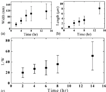
sizes共width and length兲 of the RuO2NWs was achieved by adjusting the growth time. The width, length, and the length-to-width ratio of the NWs as a function of the growth time are displayed in Figs.2共a兲–2共c兲, respectively. The width of the NWs varies linearly with the growth time initially and saturates after 8 h. The length, length-to-width ratio, and their corresponding standard deviations increase monotoni-cally with the growth time.
A schematic drawing in Fig. 3共a兲, together with a high resolution TEM image, illustrates the TEM-STM technique for our measurements of the NW resistivity at room tempera-ture. Though the nanocontact resistance is very sensitive to the interfacial structures and the NWs could be differently doped, we assume average contact resistance and NW resis-tivity in our measurements. Typical I-V curves are shown in FIG. 1.共a兲 SEM image of RuO2NWs. The inset shows a distribution of the
widths of the NWs.共b兲 High-resolution TEM image of a single-crystalline RuO2NW with its corresponding selected-area electron diffraction pattern 共inset兲.
FIG. 2.共a兲 Average width, 共b兲 average length, and 共c兲 length-to-width ratio of RuO2NWs as a function of growth time.
FIG. 3. 共a兲 Schematic illustration of the TEM-STM technique. The TEM image共right兲 displays a one nanocontact for electrical characterization. 共b兲 TEM-STM measured resistance as a function of l / A of the NWs. The inset displays the I-V curves for untreated 共nonlinear兲 and treated 共linear兲 nanocontacts.
013105-2 Liu et al. Appl. Phys. Lett. 90, 013105共2007兲
This article is copyrighted as indicated in the article. Reuse of AIP content is subject to the terms at: http://scitation.aip.org/termsconditions. Downloaded to IP: 140.113.38.11 On: Thu, 01 May 2014 01:16:50
the inset of Fig.3共b兲. Notice that the TEM-STM measure-ment produced nonlinear I-V curves for our untreated nano-contacts. We used the techniques of mechanical indentation, polishing, and focus e-beam annealing to improve the quality of the nanocontact between the NW and the electrode of a STM tip. After these treatments, we obtained linear I-V curves obeying the Ohmic law. The resistance R as a func-tion of the ratio of length共l兲 to cross-sectional area 共A兲 of the NWs was obtained and fitted with the relation R = RC+l / A,
where RCandare the nanocontact resistance and the
resis-tivity of the NW, respectively. A linear least-squares fit indi-cates Rc⬃5 k⍀ and ⬃100⍀ cm. The value is about
three times of the bulk value.
Temperature dependent resistances measured using a two-nanocontact configuration 共the inset兲 are displayed in Fig. 4. Even though the contact resistance is only on the order of 2 – 3 k⍀ 共top curve兲, the measured resistance al-ready exhibit nonmetallic behavior共at low temperatures兲 im-plying bad nanocontacts in this case. In the other case where the resistance is one order smaller共bottom curve兲, implying good nanocontacts between the NW and the electrodes, the measured resistance demonstrates metallic feature all the way down to liquid-helium temperatures. The resistivity of our NWs was determined to be 100– 300⍀ cm, which is in line with that obtained from our four-point measurements 共not shown兲 and of the same order of magnitude of that ob-tained from the STM technique. Based on the TEM-STM and e-beam results, we attribute the bad nanocontact resistance of several kilohms to the conductive rough surface formed between the NW and the electrode.24 At low tem-peratures, the rising resistance of the bad nanocontact could be fitted well with the electron hopping theory in granular
metals25possibly generated in the nanocontact.
In summary, single-crystalline RuO2 NWs with 关001兴 growth direction have been synthesized by the thermal evaporation method. The sizes of the NWs were controlled by the growth time. The TEM-STM technique provided a handy one-nanocontact measurement of the NW resistance, accompanied with a contact resistance of several kilohms. The metallic feature of the NWs can be verified by the two-nanocontact electrical characterization only when the contact resistance is at least one order of magnitude smaller than that encountered in the one-nanocontact measurement. Metallic RuO2 NWs may serve as inviting interconnects in nanoelectronics.
This work was supported by the Taiwan National Sci-ence Council under Grant Nos. NSC 94-2112-M-009-020, NSC 93-2120-M-009-009, and NSC 94-2120-M-009-010 and by the MOE ATU Program.
1N. Giordano, W. Gilson, and D. E. Prober, Phys. Rev. Lett. 43, 725
共1979兲.
2T. A. Fulton and G. J. Dolan, Appl. Phys. Lett. 42, 752共1983兲. 3J. C. Licini, G. J. Dolan, and D. J. Bishop, Phys. Rev. Lett. 54, 1585
共1985兲.
4J. J. Lin and N. Giordano, Phys. Rev. B 33, 1519共1986兲. 5N. Giordano, Phys. Rev. Lett. 61, 2137共1988兲.
6J. F. Lin, J. P. Bird, L. Rotkina, and P. A. Bennett, Appl. Phys. Lett. 82,
802共2003兲.
7S. Iijima, Nature共London兲 354, 56 共1991兲.
8M. H. Huang, S. Mao, H. Feick, H. Yan, Y. Wu, H. Kind, E. Weber, R.
Russo, and P. Yang, Science 292, 1897共2001兲.
9Z. Zhang, J. Y. Ying, M. S. Dresselhaus, J. Mater. Res. 13, 1745共1998兲. 10B. C. Satishkumar, A. Govindaraj, M. Nath, and C. N. R. Rao, J. Mater.
Chem. 10, 2115共2000兲.
11A. M. Morales and Charles M. Lieber, Science 279, 209共1998兲. 12H. Dai, E. W. Wong, and Charles M. Lieber, Science 272, 523共1996兲. 13X. Duan, Y. Huang, Y. Cui, J. Wang and Charles M. Lieber, Nature
共London兲 409, 66 共2001兲.
14Y. Cui and Charles M. Lieber, Science 291, 851共2001兲.
15H. W. C. Postma, T. Teepen, Z. Yao, M. Grifoni, and C. Dekker, Science
293, 76共2001兲.
16R. G. Vadimsky, R. P. Frankenthal, and D. E. Thompson, J. Electrochem.
Soc. 126, 2017共1979兲.
17W. D. Ryden, A. W. Lawson, and C. C. Sartian, Phys. Rev. B 1, 1494
共1970兲.
18K. M. Glassford and J. R. Chelikowsky, Phys. Rev. B 47, 1732共1993兲. 19M. L. Green, M. E. Gross, L. E. Papa, K. J. Schnoes, and D. Brasen, J.
Electrochem. Soc. 132, 2677共1985兲.
20C. C. Chen, R. S. Chen, T. Y. Tsai, Y. S. Huang, D. S. Tsai, and K. K.
Tiong, J. Phys.: Condens. Matter 16, 8475共2004兲.
21K. W. Cheng, Y. T. Lin, C. Y. Chen, C. P. Hsiung, J. Y. Gan, J. W. Yeh, C.
H. Hsieh, and L. J. Chou, Appl. Phys. Lett. 88, 043115共2006兲.
22C. Ducati, D. H. Dawson, J. R. Saffell, and P. A. Midgley, Appl. Phys.
Lett. 85, 5385共2004兲.
23M. W. Larsson, L. R. Wallenberg, A. I. Persson, and L. Samuelson,
Microsc. Microanal. 10, 41共2004兲.
24L. Kogut and K. Komvopoulos, J. Appl. Phys. 94, 3153共2003兲. 25B. Abeles, Ping Sheng, M. D. Coutts, and Y. Arie, Adv. Phys. 24, 407
共1975兲. FIG. 4. Two typical temperature dependent resistance curves obtained from
two-nanocontact electrical characterizations on single RuO2 NWs having
bad共top兲 and good 共bottom兲 nanocontacts. The inset shows SEM image of a 70 nm RuO2NW with two electrodes.
013105-3 Liu et al. Appl. Phys. Lett. 90, 013105共2007兲
This article is copyrighted as indicated in the article. Reuse of AIP content is subject to the terms at: http://scitation.aip.org/termsconditions. Downloaded to IP: 140.113.38.11 On: Thu, 01 May 2014 01:16:50