using plasma treatment
Keng-Liang Ou, Wen-Fa Wu, Chang-Pin Chou, Shi-Yung Chiou, and Chi-Chang Wu
Citation: Journal of Vacuum Science & Technology B 20, 2154 (2002); doi: 10.1116/1.1511214 View online: http://dx.doi.org/10.1116/1.1511214
View Table of Contents: http://scitation.aip.org/content/avs/journal/jvstb/20/5?ver=pdfcov Published by the AVS: Science & Technology of Materials, Interfaces, and Processing
Articles you may be interested in
Influence of N 2 O plasma treatment on microstructure and thermal stability of WN x barriers for Cu interconnection
J. Vac. Sci. Technol. B 22, 993 (2004); 10.1116/1.1715087
Ta metallization of Si–O–C substrate and Cu metallization of Ta/Si–O–C multilayer J. Vac. Sci. Technol. B 21, 293 (2003); 10.1116/1.1541606
TaC as a diffusion barrier between Si and Cu J. Appl. Phys. 91, 5391 (2002); 10.1063/1.1464652
Diffusion barrier and electrical characteristics of a self-aligned MgO layer obtained from a Cu(Mg) alloy film Appl. Phys. Lett. 77, 2192 (2000); 10.1063/1.1314879
Nanostructured Ta-Si-N diffusion barriers for Cu metallization J. Appl. Phys. 82, 4847 (1997); 10.1063/1.366346
of an amorphous layer using plasma treatment
Keng-Liang OuInstitute and Department of Mechanical Engineering, National Chiao-Tung University, Hsinchu 300, Taiwan, Republic of China
Wen-Fa Wua)
National Nano Device Laboratories, Hsinchu 300, Taiwan, Republic of China Chang-Pin Chou
Institute and Department of Mechanical Engineering, National Chiao-Tung University, Hsinchu 300, Taiwan, Republic of China
Shi-Yung Chiou
Department of Mold and Die Engineering, National Kaohsiung University of Applied Science, Kaohsiung 807, Taiwan, Republic of China
Chi-Chang Wu
National Nano Device Laboratories, Hsinchu 300, Taiwan, Republic of China 共Received 18 April 2002; accepted 12 August 2002兲
The thermal stability and electrical properties of plasma-treated TaN films have been investigated by Cu/TaN/Si systems. The properties of diffusion barrier were evaluated by sheet resistance, x-ray diffraction 共XRD兲, transmission electron microscopy 共TEM兲, x-ray photoelectron spectroscopy 共XPS兲, energy-dispersive spectroscopy 共EDS兲, Auger electron microscopy 共AES兲, and reverse-biased junction leakage current. A new amorphous layer is found to form on the surface of TaN film after the plasma treatment. Plasma-treated TaN films show better barrier performance than untreated TaN films. The sheet resistance of Cu/TaN共10 nm兲/Si increases apparently after annealing at 625 °C for 1 h, while the Cu/plasma-treated TaN共10 nm兲/Si is fairly stable up to annealing at 750 °C. The resistance to copper diffusion in plasma-treated TaN film is more effective. This is attributed that an amorphous layer that forms on the surface of TaN film after the plasma treatment. The thermal stabilities of Cu/TaN/n⫹- p junction diodes are enhanced by plasma treatment. The Cu/TaN共10 nm兲/n⫹- p and Cu/TaN共50 nm兲/n⫹- p junction diodes result in large reverse-biased junction leakage currents after annealing at 525 and 575 °C, respectively. On the other hand, plasma-treated TaN diffusion barriers improve the integrity of junction diodes up to 650 °C. Nano crystallization and stuffing effects of plasma treatments are believed to impede Cu diffusion into the Si substrate and hence improve the barrier performance. © 2002 American Vacuum Society. 关DOI: 10.1116/1.1511214兴
I. INTRODUCTION
As device dimensions become small towards 180 nm and below, interconnects will continue to be critical limitations for improving the performance and reducing costs of inte-grated circuits. Fundamental changes in existing interconnec-tion materials can increase the maximum circuit speed. Cu whose resistance is 40% lower than Al is now being intro-duced into manufacturing. However, Cu atoms can diffuse into Si devices, and degrade the device performance by in-troducing a deep level acceptor.1Typical dielectric materials used in interconnects are not effective barriers to Cu diffu-sion. In addition, Cu has poor adhesion to them. Hence, Cu interconnects are required to have both an adhesion promoter and a diffusion barrier. The microstructure of the thin-film barrier can strongly affect the texture and grain size of de-posited Cu. The preferred orientation and grain size of
cop-per are critical factors in determining electromigration reliability.2Thus, the thin barrier film is necessary to possess superior properties as mentioned above. Several diffusion barriers for Cu metallization have been investigated such as TiN,3 WN,4 Ta,5,6 and TaN.5,6 Unfortunately, most of these barriers are polycrystalline and provide inadequate protec-tion because grain boundaries may presumably serve as fast diffusion paths for copper. Among these materials, Ta–N al-loys are considered to be the most promising diffusion bar-riers for preventing Cu diffusion. Alloying Ta with N and /or O not only restricts the copper diffusion because of decora-tion of the extended defects, but also results in films with smaller grains and amorphous-like nanostructure.7
The purpose of the present investigation is twofold. The first is to prepare a thermally stable, ultrathin barrier layer between Cu and Si. TaN is selected as the barrier material in the present study because Ta has a low formation enthalpy 共⌬H兲 with nitrogen and TaN has a high melting point of 3087 °C as well as a dense structure.8Second, a method of forming nitrogen and oxygen incorporated TaN films is in-a兲Author to whom correspondence should be addressed; electronic mail:
vestigated. N2 and O2 plasmas are used to posttreat the
tan-talum nitride diffusion barriers. Properties of barrier layers are evaluated by electrical measurements and material analy-ses.
II. EXPERIMENTAL DETAILS
The substrates used in the present work were p-type共100兲 oriented silicon wafers with resistivity of 5–10⍀ cm. The Si wafers were cleaned in a dilute HF solution 共HF: H2O ⫽ 1: 20兲 for 2 min, and rinsed in de-ionized water prior to loading into the sputtering system. The 10 nm TaN films were deposited at a power of 500 W and a sputtering pres-sure of 6.4 mTorr 共0.85 Pa兲 after the base pressure was evacuated to below 5⫻10⫺7 Torr (6.67⫻10⫺5 Pa兲. The films were prepared using optimum conditions as in our pre-vious investigations, and thus provided a more effective bar-rier capability against Cu diffusion.5 Some wafers further received ex situ nitrogen or oxygen plasma treatments in a plasma enhanced chemical vapor deposition system after tan-talum nitride films were deposited. For easy identification, the untreated tantalum nitride, and nitrogen and oxygen plasma treated tantalum nitride films were denoted as TaN, TaN共N兲/TaN, and TaN共O兲/TaN, respectively. Copper films 300 nm thick were then deposited on top of the barrier layers by sputtering. Cu/TaN/Si, Cu/TaN共N兲/TaN/Si, and Cu/ TaN共O兲/TaN/Si were annealed in N2 ambient from 500 to
800 °C for 1 h to evaluate the thermal stability.
In order to analyze the properties of TaN-based barrier layers, x-ray photoelectron spectroscopy共XPS兲 using mono-chromatized Mg K␣radiation was performed to identify the chemical states of TaN films with plasma treatments. The microstructure and film thickness were examined using transmission electron microscopy 共TEM兲. Sheet resistance was measured by a four-point probe system. Film resistivity was derived from the sheet resistance and film thickness. Surface morphology of annealed Cu/barrier/Si was observed by scanning electron microscopy 共SEM兲. Compositions of failure sites were analyzed by energy dispersive spectrom-etry共EDS兲 after removing both copper and barrier layers by wet-chemical solution. Grazing incidence x-ray diffractom-etry was carried out for phase identification. The incident angle of x ray was fixed at 3°. Auger electron microscopy 共AES兲 was used to analyze the compositional depth profile after annealing. Cu/barrier/n⫹- p junction diodes with con-ventional localized oxidation of silicon isolation were fabri-cated for electrical analyses. The diode leakage current was measured by a HP4145B semiconductor parameter analyzer at a reverse bias of⫺5 V after annealing at various tempera-tures for 1 h.
III. RESULTS AND DISCUSSION
A. Properties of plasma-treated TaN films
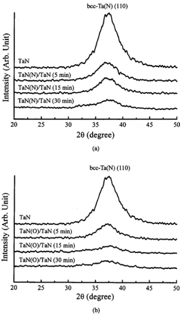
Figure 1 shows the glancing incidence x-ray diffraction spectra of 10 nm TaN films with N2or O2plasma treatments.
The time shown in the parenthesis is the time of the plasma treatment. The intensity and shape of reflections indicate
changes in the phase of the TaN film. As-deposited TaN films grow predominantly in bcc-Ta共N兲 phase and are apparently polycrystalline as determined by XRD analyses. With 5 min N2 plasma treatment, the XRD peak is considerably broad-ened, as shown in Fig. 1共a兲. It implies that the plasma treat-ment leads to a microstructural modification of the TaN bar-rier layer. With increasing N2 plasma treatment, the
enhanced broadening of the peak is observed. Similar broad-ening results are found on TaN films with O2 plasma
treat-ments, as shown in Fig. 1共b兲. Figure 2 displays cross-sectional TEM micrograph and selected area diffraction pattern of 30 min O2 plasma-treated TaN/Si 共TaN共O兲/TaN/
Si兲. Multilayered structure is observed for the TaN film with O2 plasma treatment as indicated in Fig. 2共a兲. Figure 2共b兲
demonstrates the selected area diffraction pattern taken from the region A. The electron diffraction pattern shows that the region A has a diffused ring pattern instead of diffraction spots. This indicates that the layer denoted as region A is an amorphous layer. Based on the above investigations, the de-velopment of an amorphous layer on the film surface is FIG. 1. XRD spectra of untreated and plasma-treated TaN共10 nm兲 films. 共a兲 N2plasma.共b兲 O2plasma.
clearly observed after properly inducing plasma treatment. Figure 3 shows the selected area diffraction pattern of sput-tered TaN film. Several sharp rings are observed for un-treated TaN film. It indicates that as-deposited TaN film is a
polycrystalline structure. Figure 4 shows the grain size of TaN共N兲/TaN and TaN共O兲/TaN layers as a function of plasma treatment time. The grain size is calculated from plane-view TEM. The as-deposited TaN film is a polycrystalline struc-ture with a grain size of⬃20 nm. The grain size decreases with increasing plasma treatment time. It indicates that nano-crystallization effect would occur due to the reactions and bombardments of energetic radicals and ions during plasma treatment. Moreover, it is found that grain size of the TaN共O兲/TaN film decreases more than that of the TaN共N兲/ TaN film after same plasma treatment time. That is, enhanced nano-crystallization effect on TaN共O兲/TaN barrier is found compared to TaN共N兲/TaN barrier. The grain size of the TaN film with 30 min O2 plasma treatment is only ⬃2 nm, as
shown in Fig. 4. It is reported that the nanostructured amor-phous diffusion barrier, defined as a very short range order single crystal, is highly attractive due to its relatively higher thermal stability against Cu diffusion.9
Chemical bonding states of TaN films were analyzed by XPS. Figure 5 shows the N 1s spectra of TaN films with various N2 plasma treatments and can give information
con-cerning nitridation effects. The peaks at ⬃398 eV are
ob-FIG. 2. 共a兲 Cross-sectional TEM micrograph of 30 min O2plasma-treated TaN/Si.共b兲 Selected area diffraction pattern in region A.
FIG. 3. Selected area diffraction pattern of untreated TaN film.
FIG. 4. Grain size of TaN共N兲/TaN and TaN共O兲/TaN films as a function of plasma treatment time.
FIG. 5. N 1s XPS spectra obtained from the TaN films with various nitrogen
served in the N 1s spectra for TaN films. It is consistent with the N 1s binding energy of the nitride compound.10,11 The presence of the N 1s peak in curve共b兲 in Fig. 5 clearly shows that the surface is further nitrided by nitrogen plasma. There is another emission peak at⬃401 eV observed in N 1s spec-trum. This peak at⬃401 eV is ascribed to the nitrogen atoms or molecules present in interstitial sites. This kind of nitrogen is also detected in tungsten film prepared by the reduction of WF6 with N2 in nitrogen gas.10As the N2 plasma treatment time increases to 30 min, the emission peak at⬃401 eV is dominated in the N 1s spectrum. These results indicate that some N atoms do not form strong covalent or ionic bonds with Ta atoms during the plasma nitridation of Ta film. Some of the introduced N atoms segregate at the interstitial sites and grain boundaries in the tantalum film as impurities. Similar results were reported for plasma nitridation of chemical vapor deposited tungsten by Chang et al.11 Chemi-cal compositions of untreated and N2 plasma-treated TaN
films were analyzed by XPS and presented in Table I. It is obvious that nitrogen content increases with the increasing nitrogen plasma treatment time. Nitrogen content of un-treated TaN film is 40.3 at. %. With 30 min nitrogen plasma treatment, nitrogen content increases to 63.4 at. %. Figure 6 shows O 1s XPS spectra of TaN films after O2 plasma
treat-ments for various durations. Oxygen bonding states are in-creasingly observed with increasing O2 plasma treatment, as
shown in Fig. 6. The position of the O 1s level is not clearly observed for the 5 min O2plasma-treated TaN film. The peak
of binding energy corresponding to oxygen bonding can be
observed for the TaN films with 15 min O2 plasma treat-ments. Ta–N–O compound is believed to form after the O2
plasma treatment.
Normalized resistivity of TaN共N兲/TaN film as a function of plasma treatment time is plotted in Fig. 7. The resistivity of untreated TaN film is set to be one. The normalized resis-tivity initially increases with increasing N2plasma treatment
time and then becomes constant after 10 min plasma treat-ment as shown in Fig. 7. Nitridation and nano-crystallization effects are believed to result in increase in the resistivity. In our previous study, it was found that sputtered Ta films had a resistivity of 197 ⍀ cm and resistivity of the reactively sputtered TaN film would initially decrease to 159 ⍀ cm and then increase to higher than 3500 ⍀ cm as nitrogen flow ratio increased during reactive sputtering.5 As men-tioned in experimental details, TaN films with low resistivity of 159 ⍀ cm were prepared and used in this work. It is expected that resistivity of TaN共N兲/TaN film would increase because a high-resistance surface layer forms and thus the effective thickness of the TaN film with low resistivity re-duces. However, the increase of the resistivity is slight 共⬃6%兲 and the resistivity is about 170⍀ cm which is much lower than that of the reactively sputtered TaN film with high nitrogen concentration. Though the detailed mechanisms are needed to be further investigated, the resistivity becomes constant probably because the thickness of the surface layer saturates after 10 min N2 plasma treatment. Normalized re-sistivity of TaN共O兲/TaN film is higher than that of TaN共N兲/ TaN film. The increase of the resistivity may be due to the formation of high-resistance Ta–O compound. However, the resistivity of TaN共O兲/TaN film is still much lower than that of the reactively sputtered TaN film with high nitrogen con-centration.
B. Thermal stability of CuÕbarrierÕSi system
Cu/barrier/Si systems annealed at various temperatures were characterized by sheet resistance. Figure 8 shows varia-tion of sheet resistance of Cu/barrier/Si as a funcvaria-tion of an-nealing temperature. The variation of sheet resistance is de-signed as the ratio of (R-Ro) to Ro, where Ro and R denote
TABLEI. Compositions of N2plasma-treated TaN共TaN共N兲/TaN兲 films. Plasma treatment time
共min兲 Ta共at. %兲 N共at. %兲
0 59.7 40.3
5 52.1 47.9
15 48.2 52.8
30 34.6 63.4
FIG. 6. O 1s XPS spectra obtained from the TaN films with various oxygen
plasma treatments.
FIG. 7. Normalized resistivity of TaN共N兲/TaN film as a function of plasma treatment time.
the sheet resistance of as-deposited and annealed sample, respectively. The results reflect interactions between Cu and Si indirectly. The data mainly indicate changes in the thick-ness or resistivity of the unreacted copper layer, since the resistance of the barrier layer and reaction products are ex-pected to be much larger than that of Cu. An abrupt increase of sheet resistance occurs and the surfaces become gray for the samples with sputtered TaN共10 nm兲 and TaN共50 nm兲 bar-riers after annealing at 625 and 650 °C, respectively. This implies that Cu has diffused into silicon substrate. Tsai et al. reported similar results. An obvious increase was found for the sheet resistance of the Cu/physical vapor deposition TaN共60 nm兲/Si system after annealing at 650 °C for 30 min.12 Sheet resistance of the samples with 30 min plasma-treated TaN barrier layers only increases a little after anneal-ing at 750 °C for 1 h, as shown in Fig. 8. It is obvious that thermal stability of TaN barrier can be increased by plasma treatment.
Figure 9 shows the XRD spectra for Cu/TaN/Si samples after annealing at various temperatures for 1 h. Figure 9共a兲 clearly shows the formation of copper silicide (Cu3Si兲 for the Cu/TaN共10 nm兲/Si sample after annealing at 625 °C. The results are consistent with the abrupt increase in the sheet resistance as shown in Fig. 8. Strong Ta2N and TaN peaks
are found for the samples with 50 nm TaN barrier layers after annealing at higher than 600 °C. The peaks of Cu3Si are
observed after annealing at 650 °C, as shown in Fig. 9共b兲. Failure of barrier layer is attributed to enhanced crystalliza-tion of the TaN film after high-temperature annealing. On the other hand, the peak of copper silicide is not observed for the sample with 10 nm TaN共N兲/TaN or TaN共O兲/TaN barrier layer annealed at 700 °C, as shown in Fig. 10. It is obvious that plasma treated TaN barrier possesses higher thermal stability and can impede Cu diffusion into the Si substrate. Additional results have been obtained in AES depth profiles. Figure 11 shows the AES depth profiles of Cu/TaN共O兲/TaN/Si after an-nealing at 700 °C for 1 h. As is expected from results of XRD and sheet resistance, no significant interdiffusion is observed between Cu and Si. It reveals that plasma-treated TaN barrier possesses excellent barrier performance.
SEM was used to examine the surface morphologies after thermal annealing for further analyzing thermal stability. Protrusions or precipitates are observed on the surface after annealing at the temperature that an abrupt increase of sheet resistance occurs. Figure 12 shows the SEM micrograph and chemical composition analyses of the sample with TaN共O兲/ TaN barrier film after annealing at 750 °C for 1 h. Figure 12共a兲 shows surface morphology of silicon substrate after copper and tantalum nitride are stripped. It reveals local de-fect sites, as denoted as region B in Fig. 12共a兲. EDS is further employed to analyze the chemical compositions in region B. The concentrations of copper and silicon are 74.23 and 25.77 at. %, respectively. It is evident that the ratio of Cu to Si approximates 3 in region B. Distributions of Cu and Si in region B are further analyzed by mapping. Copper is uni-formly distributed as shown in Fig. 12共c兲. Figure 12共d兲 shows the mapping of silicon. Less silicon is observed in region B. It reveals that copper has already penetrated the barrier film into silicon substrate after annealing at 750 °C FIG. 8. Variation of sheet resistance of Cu/barrier/Si system as a function of
annealing temperature.
FIG. 9. XRD spectra of Cu/TaN/Si systems after annealing at various tem-peratures for 1 h.共a兲 10 nm. 共b兲 50 nm.
and copper silicide forms as Cu3Si. From the results of sheet
resistance and SEM, the abrupt increase of resistance is as-cribed to the formation of Cu3Si compound in Si substrate. The results of SEM and EDS are in good agreement with the sheet resistance.
C. Electrical properties of CuÕbarrierÕn¿-p diodes
Barrier capabilities of TaN共10 nm兲, TaN共50 nm兲, TaN共N兲/ TaN共10 nm兲, and TaN共O兲/TaN共10 nm兲 films are further in-vestigated by evaluating the integrity of Cu/barrier/n⫹- p junction diodes after stressing by thermal annealing. Figure 13 illustrates the statistical distributions of reverse biased leakage current densities measured at ⫺5 V for Cu/barrier/
n⫹- p junction diodes annealed at various temperatures. With a failure criterion of 10⫺6A/cm2, the Cu/TaN共10 nm兲/n⫹- p diodes remain stable after annealing at temperatures up to 500 °C but suffer degradation at 525 °C as shown in Fig. 13共a兲. Figure 13共b兲 shows the statistical distributions of re-verse biased leakage current densities for the Cu/TaN共50 nm兲/n⫹- p junction diodes annealed at various temperatures. The diodes remain stable after annealing at temperature up to
550 °C for the diodes with 50 nm TaN barriers. Failure of the diode is observed after annealing at 575 °C. Thermal stability of the Cu/TaN/n⫹- p junction diode is found to be dependent on the thickness of the barrier layer. As thickness of the TaN barrier layer increases from 10 to 50 nm, the failure tempera-ture is increased ⬃50 °C. However, as the devices become smaller and dimensions decline below 180 nm, it becomes inappropriate to use a barrier layer thicker than 30 nm. The barrier thickness should be reduced to lower the resistance of the total line interconnect and/or via. As mentioned previ-ously, N2 and O2 plasma treatments are used to improve barrier capabilities of ultrathin TaN layers 共10 nm兲. The Cu/ TaN共N兲/TaN/n⫹- p diodes remain stable after annealing at 550 °C, as shown in Fig. 13共c兲. Moreover, most Cu/TaN共N兲/ TaN/n⫹- p diodes have low junction leakage currents even after thermal stressing at 650 °C. The TaN共N兲/TaN films pos-sess much better barrier performance than untreated TaN films. Figure 13共d兲 shows the statistical distributions of re-verse biased leakage current densities for Cu/TaN共O兲/TaN共10 nm兲/n⫹- p junction diodes annealed at various temperatures. Highly improved barrier capability against Cu diffusion is observed since low leakage currents are obtained for Cu/ TaN共O兲/TaN 共10 nm兲/n⫹- p junction diodes even after an-nealing at 650 °C for 1 h. Improved barrier performance is attributed to nano-crystallization and stuffing effects due to the reactions and bombardments of energetic radicals and ions during plasma treatment. It is reported that the micro-structure within the barrier layer strongly affects the barrier performance because Cu diffuses through fast diffusion paths such as grain boundaries within the barrier layer.5,6,13 The thin amorphous TaNxand TaNxOylayers form on the surface
of the TaN films after nitrogen and oxygen plasma treat-FIG. 10. XRD spectra of Cu/TaN共N兲/TaN共10 nm兲/Si and Cu/TaN共O兲/TaN共10
nm兲/Si systems after annealing at 700 °C for 1 h.
FIG. 11. AES compositional depth profiles of Cu/TaN共O兲/TaN/Si after
an-nealing at 700 °C.
FIG. 12. 共a兲 SEM micrograph of Cu/TaN共O兲/TaN/Si sample annealed at 750 °C for 1 h.共b兲 EDS spectrum obtained from region B in Fig. 12共a兲. Mapping analyses for共c兲 Cu and 共d兲 Si in region B.
ments. Amorphous diffusion barrier is more effective for pre-venting Cu diffusion than the polycrystalline barrier since the amorphous film does not have large-angle grain boundaries where most of the atomic diffusion typically occurs.9 More improved barrier performance is found for TaN共O兲/TaN bar-rier due to enhanced nano-crystallization effect compared to TaN共N兲/TaN barriers.
IV. CONCLUSION
The effectiveness of tantalum nitride with N2 or O2
plasma treatment as a diffusion barrier between copper and silicon has been investigated. An amorphous layer is found to form on the surface of the TaN film after the plasma treat-ment. The oxygen and nitrogen bonding states are observed for O2 and N2 plasma-treated TaN films. Thermal stabilities
of plasma-treated barriers TaN共N兲/TaN and TaN共O兲/TaN are better than those of untreated barriers TaN共10 nm兲 and TaN共50 nm兲. Nano-crystallization and stuffing effects as well as nitridation and oxidation are observed. A new amorphous layer can be induced on the surface of the TaN barrier with
the reactions and bombardments of nitrogen or oxygen radi-cals and ions. The barrier performance of the TaN film is improved apparently after plasma treatment. The Cu/TaN共N兲/ TaN共10 nm兲/Si and Cu/TaN共O兲/TaN共10 nm兲/Si contact sys-tems remain stable after annealing at 700 °C for 1 h. Thermal stability and electrical integrity of Cu/TaN/n⫹- p junction di-odes are enhanced by plasma treatment. The failure tempera-ture of the sample with plasma-treated TaN barrier is about 150 °C higher than that of the sample with untreated TaN barrier. Nano-crystallization and stuffing effects of plasma treatments are believed to impede Cu diffusion into the Si substrate and hence improve the barrier performance. More improved barrier performance is found for TaN共O兲/TaN bar-rier due to enhanced nano-crystallization effect compared to TaN共N兲/TaN barrier.
ACKNOWLEDGMENT
The authors would like to thank the National Science Council of the Republic of China for financially supporting FIG. 13. Statistical distributions of reverse-biased leakage current densities for共a兲 Cu/TaN共10 nm兲/n⫹- p,共b兲 Cu/TaN共50 nm兲/n⫹- p,共c兲 Cu/TaN共N兲/TaN共10 nm兲/n⫹- p, and共d兲 Cu/TaN共O兲/TaN共10 nm兲/n⫹- p junction diodes annealed at various temperatures for 1 h.
this research under Contract Nos. NSC 90-2215-E-317-005 and NSC 91-2722-2317-200.
1Y. J. Lee, B. S. Suh, M. S. Kwon, and C. O. Park, J. Appl. Phys. 85, 1927 共1999兲.
2
Y. L. Chin, B. S. Chiou, and W. F. Wu, Jpn. J. Appl. Phys., Part 1 39, 6708共2000兲.
3T. Kouno, H. Niwa, and M. Yamada, J. Electrochem. Soc. 145, 2164 共1998兲.
4
M. Uekubo, T. Oku, K. Nii, M. Murakami, K. Takahiro, S. Yamaguchi, T. Nakano, and T. Ohta, Thin Solid Films 286, 170共1996兲.
5W. L. Yang, W. F. Wu, D. G. Liu, C. C. Wu, and K. L. Ou, Solid-State Electron. 45, 149共2001兲.
6K. H. Min, K. C. Chun, and K. B. Kim, J. Vac. Sci. Technol. B 14, 3263 共1996兲.
7M. Stavrev, D. Fischer, C. Wenzel, K. Drescher, and N. Mattern, Thin Solid Films 307, 79共1997兲.
8T. Oku, E. Kawakami, M. Uekubo, K. Takahiro, S. Yamaguchi, M. Mu-rakami, S. Yamaguchi, and M. MuMu-rakami, Appl. Surf. Sci. 99, 265共1996兲. 9
D. J. Kim, Y. T. Kim, and J. W. Park, J. Appl. Phys. 82, 4847共1997兲. 10T. Nakajima, K. Watanable, and N. Watanabe, J. Electrochem. Soc. 134,
3175共1987兲.
11K. M. Chang, T. H. Yeh, I. C. Deng, and C. W. Shih, J. Appl. Phys. 82, 1469共1997兲.
12M. H. Tsai, S. C. Sun, C. E. Tsai, S. H. Chuang, and H. T. Chiu, J. Appl. Phys. 79, 6932共1996兲.
13G. S. Chen and S. T. Chen, J. Appl. Phys. 87, 8473共2000兲.