cDepartment of Physics, Clarendon Laboratory, University of Oxford, Parks Road, Oxford OX1 3PU, UK
Received 3 November 1999; received in revised form 30 November 2000; accepted 15 December 2000 by P. Sheng
Abstract
We report a magneto optical characterization of InGaAs/GaAs quantum well (QW) and quantum dot (QD) structures grown on (111)B GaAs substrates. The photoluminescence (PL) peak shift under high excitation intensity is used to distinguish QW from QD structures together with atomic force microscopy (AFM) imaging. The binding energy in (111)InGaAs/GaAs QW is about 5 meV. The extent of the wave function obtained from the diamagnetic shift of the PL peak energy is consistent with the result calculated by the k.p method. The InGaAs/GaAs QD lateral con®nement energy and the dot size are also estimated from the diamagnetic shift of the PL lines. The lateral con®nement energy is estimated as 7 meV. The mean radius of the InGaAs QD is about 14 nm and the dot height is about 6 nm, which is in good agreement with the results as revealed in AFM imaging. q 2001 Published by Elsevier Science Ltd.
Keywords: A. Quantum wells; A. Nanostructures; D. Optical properties; E. Luminescence PACS: 78.20.Ls
1. Introduction
Low-dimensional semiconductor microstructure such as quantum well (QW) has attracted much interest during the past decades, due both to the potential applications and to the interesting basic physics for opto-electronic devices. As a material for microelectronics and opto-electronics, InGaAs/GaAs QW structures have received attention due to the low effective mass of the carrier [1,2] and to the high optical gain [3]. Since semiconductor quantum dots (QDs) were suggested to improve the performance of opto-electronic device [4,5], there has been a variety of researches on fabrication techniques. The most popular method in QD fabrication is the Stranski±Krastanov (S±K) growth mode, utilizing strain relaxation between two materials with large lattice mismatch to facilitate the island growth. The fabrication of QDs using the S±K growth mode on (100) and (111)BGaAs substrates have been
reported [6±8]. However, the control of growth conditions is critical for good uniformity of QDs. In our previous work [9], we had reported a simple method to fabricate high qual-ity InGaAs/GaAs QDs on (111)BGaAs substrates by lower-ing the substrate temperature. The QW structure was grown at higher substrate temperature, while the QD structure fabricate, as the substrate temperature was lowered down. The formation of the QDs was identi®ed by the atomic force microscopy (AFM) image.
Magneto-optics in high magnetic ®elds is a powerful tool to investigate the electronic states in low-dimen-sional systems. In this article, we report magneto-photo-luminescence (PL) measurement on InGaAs/GaAs QW and QD structures on (111)B substrate. From the high excitation-intensity PL spectra, the structure of the sample could be categorized as QW or QD and is consistent with the results found in AFM images. The exciton binding energy deduced from the diamagnetic shift of the PL peak energy is about 5 meV. The k.p theory was employed in calculating the QW transition energy. The wave function calculated is consistent with that obtained from the diamagnetic shift of PL line. In
0038-1098/01/$ - see front matter q 2001 Published by Elsevier Science Ltd. PII: S0038-1098(01)00018-7
* Corresponding author. Tel.: 2088952; fax: 1886-6-2747995.
addition, the in-plane dot con®nement energy and dot size are also estimated from the diamagnetic shift of the PL energy.
2. Experiment
A schematic cross-section of the sample is shown in
Fig. 1. GaAs(111)B substrates with 28 off toward (211) were used. A GaAs buffer layer of 300 nm was ®rst grown at a substrate temperature of 5908C. Next, a In0.25Ga0.75As layer with a nominal thickness of 1.5 nm
was grown. Before the growth of this layer, the substrate temperature was lowered during a growth interruption. Three different growth temperatures of 525, 515, 4508C were used for growing this layer. Samples A, B, and C correspond to these three growth conditions, respectively. Finally, a cap layer of 50 nm GaAs was grown. All layers were undoped. Samples A, B are QW structures, sample C can be identi®ed as QD structure for small islands, revealed in the AFM image [9]. Another set of reference samples with the same structures but different substrate, GaAs(100), were grown simultaneously at each growth temperature.
Magneto-PL spectra were measured using an Oxford Instruments superconducting solenoid magnet system in ®eld up to 15 T at 4.2 K in both Faraday (B k z) and the
Fig. 1. A schematic cross-section of the sample. All layers are undoped.
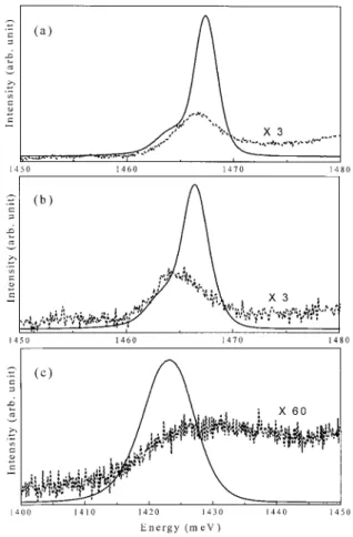
Fig. 2. PL spectra for samples A, B and C under low (solid lines) and high (dash lines) excitation intensity.
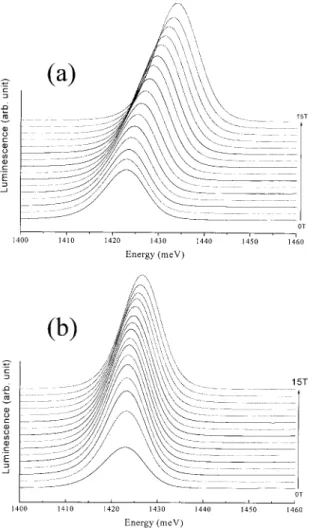
Fig. 3. The magneto-PL spectra in 1 T separation for sample A in (a) Faraday and (b) Voigt con®gurations.
Voigt con®gurations (B ' z), where z denotes the growth direction. The PL spectra were obtained by a quarter meter spectrometer. The 690 nm line of a 10 mW solid laser is used for the illumination giving a maximum intensity of ,1022W cm22. For the high
intensity PL measurement, a 4 ns pulse laser emitting at l 266 nm at 10 Hz and with a maximum energy per pulse of 0.4 mJ was used, giving illumination inten-sities of 105cm22.
3. Results and discussions
Fig. 2 shows the PL spectra for all samples measured under low CW (solid lines) and high (dash lines) pulsed excitation intensities at 4.2 K. The high power spectra were considerably noisier due to the low repetition rate (10 Hz) of the pulsed laser excitation. The transition energy, EP, for low intensity pumping in the vicinity of 1467 meV in
Fig. 2(a) results from exciton emission, the shoulder in the
as sample A. The PL spectrum measured from sample C is shown in Fig. 2(c). The transition energy is about 1423 meV and the HWHM is 4.5 meV indicating excellent quality. On the contrary, the peak energy shifts to higher energy when the excitation intensity increased. The blue shift of the emis-sion line is a clear indication of size quantization effect, which is caused by the inhomogeneous distribution of the dot sizes [14]. These spectra were another evidences in distinguishing the QW and QD structures and consistent with the results shown in the AFM image [9].
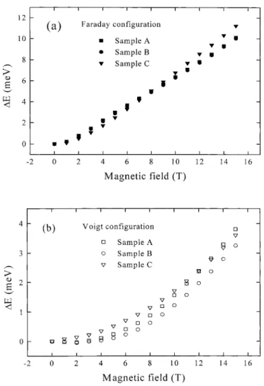
Fig. 3 shows the magneto-PL spectra in 1 T separa-tion from QW sample A in both Faraday and Voigt con®gurations, respectively. Fig. 4 shows the magneto-PL spectra from QD sample C in both con®gurations. Both QW and QD peaks shift diamagnetically to the higher energy side, as the intensity of magnetic ®eld increases. The shoulder of the peak in QW spectra disappears as the strength of magnetic ®eld increases. Fig. 5 shows the diamagnetic shifts, DE, of the of the PL lines for all samples in both con®gurations. The peak positions were obtained from Gaussian lineshape ®tting. The diamagnetic shifts in the Voigt con®guration are smaller than that in the Faraday con®guration because of the stronger con®nement in the growth direc-tion. In the low-®eld region of Faraday con®guration, the ®eld dependence of the PL shift is quadratic for the diamagnetic shift of the exciton. With increasing magnetic ®eld, the peak energy shifts linearly, because the cyclotron energy associated with the magnetic ®eld overcomes the Coulomb energy.
In order to obtain the exciton binding energy, Eb, in QW
structure, the exciton reduced mass should be obtained at ®rst. The heavy-hole effective mass for In0.25Ga0.75As/GaAs
QW in the (100) direction was determined as 0.23m0(m0is
the free electron mass) by extrapolation from values reported in previous articles [15±17]. Because the spin-splitting energy is much smaller than the fundamental tran-sition energy and assumed that, the Kane matrix elements of InAs and GaAs are the same. The electron effective mass for In0.25Ga0.75As/GaAs QW in the (100) direction can be
esti-mated as 0.064m0by Kane's theory [18] after the measured
transition energy of the InGaAs QW is taken into account. In QW structures, the wave functions of the electron and hole leak out far beyond the well because of the thin well width; therefore, a three-dimensional exciton model can be used to evaluate exciton binding energy. Fitting the low ®eld
Fig. 4. The magneto-PL spectra in 1 T separation for sample C in (a) Faraday and (b) Voigt con®gurations.
diamagnetic shift of the reference QW samples grown in (100) direction (not shown), to the numerical calculations of Makado [19] and using the exciton reduced mass m100 0:050m0obtained above, the binding energy can be
deduced as ,7 meV. This value is in good agreement with the result of Moore et al. [16].
The exciton reduced mass,m111, for InGaAs/GaAs QW in
the (111) direction, was obtained by the relation [20]
b100=b1111=3m111=m100; 1
whereb100andb111denote the diamagnetic shift coef®cient
in the (100) direction and the (111) direction, respectively. The value ofm111was evaluated as 0.042m0from Eq. (1).
For the samples grown in the (111) direction and using the same method with m111 0:042m0, the exciton binding
energy for sample C is found to be smaller with a value of ,5 meV. The binding energy for the (111) direction growth is smaller than that for the (100) direction due to the internal electric ®elds, which tilt the con®nement potentials and
displace the con®ned wave functions, with the electron and hole states spatially localized at opposite sides of the well layers.
The transition energy at B 0 can be calculated by
EP Eg1 11H 2 Eb; 2
where Eg and 11H are the band-gap, and the transition
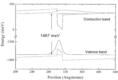
energy from the ®rst conduction to the ®rst valence subband of heavy hole character, respectively. We have used a 4-band k.p perturbation method to calculate the transition energy. There are two factors which should be considered: the strain effect produced by the high indium concentration and the internal piezoelectric ®eld induced by non-zero diagonal components of the strain in the (111) orientation. The parameters are obtained by interpolation of InAs and GaAs [21] and the band-offset Qvis 0.15 [22]. The transition
energy calculated for a 15 AÊ well width is 1457 meV. This value is smaller than the observed value of 1467 meV. If the well width is reduced to 12 AÊ, agreement is found with the
observed transition energy, as shown in Fig. 6. To a good approximation, it is reasonable to assign a well width of ,12 AÊ for QW samples.
The diamagnetic shift of the exciton peak at low ®eld can be represented by [23,24]
DE e2kr2l=8mB2; 3
where kr2l1=2 represents the extent of the con®ned wave function (ECWF) and the exciton reduced mass is assumed to be similar to that of previously used for (111) oriented structures. The diamagnetic coef®cients for sample A are ,136 meV T22, ,17 meV T22for B
kand B', respectively.
Using these values and Eq. (3), the in-plane ECWFs, krxryl1=2; then the ECWFs in z direction, krzl; can be obtained as 16.2 and 2.1 nm, respectively, which is consis-tent with the results as shown in Fig. 6.
The diamagnetic coef®cients for sample C are ,109 meV T22 and ,15 meV T22 for B
kand B',
respec-tively. As mentioned above, we can use Eq. (3) to evaluate ECWFs. Using the values above gives krxryl , 208 nm2for the area of the in-plane ECWF and krxrzl , 31 nm2for a cross-section through the dot. This suggests a mean dot radii of ,14 nm and an aspect ratio of ,0.15. This corresponds to a dot height of ,6 nm. The value is in good agreement with the result, 5 nm, obtained by AFM technique [9]. There will be considerable wave function penetration into the barrier for such a relatively weakly con®ned dot as studied here, and as a result the value is an overestimate relative to direct physical measurements such as AFM.
Assuming the in-plane con®ning potential of the dot is a parabolic potential
V 1
2mv2rr2: 4
In the Faraday con®guration, the ground state energy shift of
the dot can be expressed as [25,26] DE 1 2" v2 c1 4v2r q ; 5
where vc eB=m is the electron cyclotron frequency and 2"vrgives the in-plane dot con®nement energy. By ®tting the Eq. (5) to the experiment data, the lateral con®nement energy can be estimated as 2"vr 7 meV. The con®ne-ment in the in-plane direction deduced is substantial but much less than that in the growth direction. The lateral size of the dot con®ned wave function is also consistent with the magnetic ®eld at which the energy shift changes over to a linear increase in energy with ®eld in the Faraday case. The con®nement effects are negligible at this point and the cyclotron radius is approximately equal to the dot radius. Taking this ®eld to be 4 T, the radius can be estimated as ,13 nm.
4. Conclusions
In conclusion, we have used high intensity PL measure-ments to con®rm the structures of InGaAs layer grown in (111) direction at different temperatures. A red shift of the peak indicates a QW structure grown at high temperatures while a blue shift is found for QD structure grown at low temperature in agreement with the conclusions reached using AFM. The ECWF of the QW estimated from the excitonic diamagnetic shift is consistent with the results calculated by k.p theory. The exciton binding energy for InGaAs/GaAs QW in the (111) direction is about 5 meV. The InGaAs/GaAs QD lateral con®nement energy and the dot size are estimated from the diamagnetic shift. The size of the dots deduced from magneto-PL is in agreement with the results of AFM.
Acknowledgements
This work was supported by the National Science Council of the Republic of China under Contract No. NSC89-2112-M006-038.
References
[1] D.C. Reynolds, K.R. Evans, K.K. Bajaj, B. Jogai, C.E. Stutz, P.W. Yu, Phys. Rev., B 43 (1991) 1871.
[2] J. Sanchez-Dehesa, J.L. Sanchez-Rojas, C. Lopez, R.J. Nicho-las, Appl. Phys. Lett. 61 (1992) 1072.
[3] E. Fortin, B.Y. Hua, A.P. Roth, A. Charlebois, S. Fafard, C. Lacelle, J. Appl. Phys. 66 (1989) 4854.
[4] Y. Arakawa, H. Sakaki, Appl. Phys. Lett. 40 (1982) 939. [5] H. Sakaki, Jpn. J. Appl. Phys. 49 (1986) 1043.
[6] D.I. Lubyshev, P.P. Gonzalez-Borrero, E. Marega Jr, E. Petit-prez, N. La Scala Jr, P. Basmaji, Appl. Phys. Lett. 68 (1996) 205.
[7] D. Leonard, M. Krishnamurthy, C.M. Reaves, S.P. Denbaars, P.M. Petroff, Appl. Phys. Lett. 63 (1993) 3203.
[8] D.I. Lubyshev, P.P. Gonzalez-Borrero, E. Marega Jr, E. Petit-prez, P. Basmaji, J. Vac. Sci. Technol., B 14 (1996) 2212. [9] F.Y. Tsai, C.P. Lee, J. Appl. Phys. 84 (1998) 2624. [10] A. Patane, A. Polimeni, M. Capizzi, F. Martelli, Phy. Rev., B
52 (1995) 2784.
[11] P.B. Kirby, J.A. Constable, R.S. Smith, Phys. Rev., B 40 (1989) 3013.
[12] S. Tarucha, H. Kobayashi, Y. Horikoshi, H. Okamoto, Jpn. J. Appl. Phys. 23 (1984) 874.
[13] D.S. Chemla, D.A.B. Miller, P.W. Smith, A.C. Gossard, W. Wieqmann, IEEE J. Quantum Electron. QE-20 (1984) 265.
[14] F. Daiminger, A. Schmidt, K. Pieger, F. Faller, A. Forchel, Semicond. Sci. Technol. 9 (1994) 896.
[15] N.J. Pulsford, R.J. Nicholas, R.J. Warburton, G. Duggan, K.J. Moore, K. Woodbridge, C. Roberts, Phys. Rev. B 43 (1991) 2246.
[16] K.J. Moore, G.D. Duggan, K. Woodbridge, C. Boberts, Phys. Rev. B 41 (1990) 1090.
[17] H.Q. Hou, Y. Segawa, Y. Aoyagi, S. Namba, J.M. Zhou, Phys. Rev. B 42 (1990) 1284.
[18] G. Bastard, J.A. Brum, R. Ferreira, in: H. Ehrenreich, D. Turn-bull (Eds.), Solid State Physics, Vol. 44, Academic Press, New York, 1991, p. 234.
[19] P.C. Makado, Physica 132 B (1985) 7.
[20] S.H. Pan, H. Shen, Z. Hang, F.H. Pollak, W. Zhuang, Q. Xu, A.P. Roth, R.A. Masut, C. Lacelle, D. Morris, Phys. Rev. B 38 (1988) 3375.
[21] Landolt-BoÈrnstein, in: O. Madelung (Ed.), Numerical Data and Functional Relationships in Science and Technology, New series group III, Vol. 22a, Springer, Berlin, 1987, p. 63 (see also p. 117).
[22] D.J. Arent, Phys. Rev. B 41 (1990) 9843.
[23] R.K. Hayden, K. Uchida, N. Miura, A. Polimeni, S.T. Stod-dart, M. Henini, L. Eaves, P.C. Main, Phys. B 249 (1998) 262. [24] R. Rinaldi, R. Mangino, R. Cingolani, H. Lipsanen, M. Sopa-nen, J. Tulkki, M. Brasken, J. Ahopelto, Phys. Rev. B 57 (1998) 9763.
[25] P.D. Wang, J.L. Mertz, S. Farad, R. Leon, D. Leonard, G. Medeiros-Ribeiro, M. Oestreich, P.M. Petroff, K. Uchida, N. Miura, H. Akiyama, H. Sakaki, Phys. Rev. B 53 (1996) 16458. [26] G. Bastard, Wave Mechanics Applied to Semiconductor Heterostructures, les editions de physique, Les Ulis, 1996, pp. 317±325.