IMPROVED HOT CARRIER
RELIABILITY
IN
STRAINED-CHANNEL
NMOSFETS WITH TEOS BUFFER
LAYER
Ching-SenLu',Homg-Chih Lin'2 Yao-JenLee2, andTiao-YuanHuang'
'Departmentof Electronics Engineering and Institute of Electronics,National ChiaoTungUniversity,
1001 TaHsueh Road, Hsinchu, Taiwan300,R.O.C
2National
NanoDeviceLaboratories, 26 ProsperityRoadI, Science-based IndustrialPark, Hsinchu,Taiwan30078, R.O.C.Phone:886-3-571-2121 ext:54193, Fax: 886-3-572-4361,e-mail:
hclingfaculty.nctu.edu.tw
INTRODUCTION
Since local tensile strain technology with SiN CESL has emergedas oneof themosteffective methodstoboost the drive
current inscaled NMOS devices [1,2], attention shouldnowbe focused on the device reliability associated with the strained devices, as the increased substrate current due tothe strain and
excess hydrogen incorporation from the deposited SiN layer couldpotentially aggravate the hot-electron effects. Although the physical mechanisms and characteristics of hot electron degradation have beenextensively studied [3,4], thereseems tobe veryfew worksinvestigating the impact of SiN capping layer and the associated deposition processonthe hot carrierreliability of the strained devices. Inthis work, we investigate this issue and proposetheincorporation ofathin TEOSbufferlayertoimprove thereliability performance.
DEVICE FABRICATION
NMOSFETs characterized in this study have agateoxide thickness of 3 nmand a 150nm-thick n+poly-Si gate electrode. After the gate formation, most wafers were capped with a
300nm-thick LPCVD-SiN layer (denoted as SiN-capped split), while some wafers were deliberately skipped of the SiN deposition stepto serve as the controls (denoted as the control split). For someSiN-cappedwafers,athin LPCVD-TEOSbuffer layer (10 nmor20nm) was capped priorto the SiN deposition (denoted as BL-1OnmTEOS split and BL-20nmTEOS split, respectively). Yetinsome SiN-capped wafers, the SiN layerwas
deliberately stripped after SiNdepositioninorderto evaluate the impact of SiN deposition process itselfonthe deviceperformance (denotedasSiN-removalsplit).
RESULTS AND DISCUSSION
1-1010-2Vi/L 10[tmO.4[tm Vds-1.5V
10-3 s= 5
:S10-4
-10-5 [ Controlr_
a) 10o-6; - - - SiNCapping
~~~ 106~ ~ ~ ...BL TEOS 1Onm 10-7 BL TEOS20nm O 10-0 SiN Removal 10-1 co1010 1 0-1.0 0 1o->O-J e .... ... -0.5 0.0 0.5 1.0 1.5 VGVth(V) 600 500 400 300 200 100 0 i6 'E. (1) O c 2O 3 70 c 0 O U) c p
F--Fig. 1Subthreshold characteristics and transconductance of NMOSFETs for allsplits.
Fig. 1 shows the subthreshold characteristics and transconductance(Gm) of NMOSFETs for allsplits, with channel length of 0.4 pm. It can be seenthat all splits exhibit similar subthreshold slope. Significant increase in Gmover the control device is observed for all SiN-capped splitswithorwithout the TEOSbufferlayer, although similar enhancement isnotobserved inthe SiN-removalsplit. These resultsclearly indicate that (a) the performance enhancement arises mainly from the tensile strain inducedby the SiN layer, and(b)the insertion of 10nmor20nm thick TEOS buffer layer does not compromise the device
1 42440919
5107/$25
0002007IEEEperformance. Toconfirm these findings, output characteristics of NMOSFETs are shown and compared in Fig. 2. Drive current
enhancement over the controlsample is indeed clearly observed for the SiN-capped and BL-TEOS splits, while SiN-removal samples show negligibleimprovement.
7-6 E5 a)4 3 ,5 2 1 0-0.i Control WL OpmO4pm SiN Capping BLTEOS 1Onm g 2 BLTEOS 20nm SiN Removal g-Vt-12V Vg Vt=04V />:=..-5 = 0.5 1.0 1.5 2.0 DrainVoltage(V)
Fig. 2 Output characteristics of NMOSFETs for allsplits.
Fig. 3 shows the percentage increase of Gm for the SiN-capped, BL-TEOS, and SiN-removalsamples with respectto
the control, as a function of channellength.We can seethat the Gmenhancement reaches about33% at achannel length of 0.4 pm in the SiN-capped and BL-TEOS samples. When the SiN capping layer is removed, such enhancement diminishes. These observations demonstrate that the Gm enhancement istruly dueto
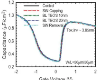
the uniaxial tensile strain induced by the SiN capping which increases withdecreasing channellength and the induced tensile strain is notjeopardizedby the TEOS buffer layer used in this study. The capacitance-voltage (C- V characteristics of the samples are shown in Fig. 4. Basically all splits show almost identical curves, indicating that the above observations are not
causedby the thickness difference among gate oxides.
40 35 30 S 25 E 20 E 15 (D 10 * SiNCapping A BLTEOS1Onm
4
* BLTEOS20nm 0 I* SiNRemoval 5 a0i00
0 Um U a 5 1 10 ChannelLength(pm)Fig. 3 Percentage increase of transconductance with respecttothe control versus channel length. Each datum point represents the mean measurementvalue from six devices.
1.2 E 1.0 LLI 0.8 a) a0.6 X0.4 C.) 0.2 Control SiNCapping BLTEOSlOnm BLTEOS2Onm SiNRemoval XTox,inv 3.85nm W/L=50pm/50lm -2 -1 0 1 2 GateVoltage(V)
Fig.4Capacitance-Voltage (C- )characteristics for allsplits.
IEEE07CH37867 45thAnnualInternational
Reliability
670 Physics Symposium, Phoenix, 2007
Next we focus our attention on the hot-carrier
characterization withanaimtoclarify whethertheuseofTEOS
buffer layer is beneficial inimproving thehot-carrier resistance. Fig. 5 shows substrate current (ISUb) versus gate voltage for all
splits. Itcanbeseenthat the substratecurrentofthe SiN-capped
split and the BL-TEOS splits show similar trends, andare larger
than that of the controlcounterpart.This result indicatesthat the
channel strain playsanimportant roleinaffecting the generation
of channel hot electrons.Inaddition, athin10nmor20nm TEOS
buffer layer does not seem to release the stress by the SiN capping because of the similar maximum substrate current
(Isub,max).
This could be relatedto thebandgap
narrowing
effect induced by the channel strain aswell asthe increased mobility,both tend to enhance the impact ionization rate [5,6], and may
potentially worsen the hot-electron degradation in the strained
devices [7]. InFig. 5, it is alsointerestingto notethatIsubinthe
SiN-removalsampleis alsolargerthan that in thecontrol device. This could be explained by the additional hydrogen species by the
SiN depositionprocess that tends toreduce theimplant damage locatednearthe drain region.
0.7 < 06 0.5 0.4 0 0.3 0.2 I 0.1 0.0
eliminated by the SiN removal. This phenomenon clearly indicates that the SiN depositionprocessitselfmayresult in the
enhanced damage effect in the short-channel devices. However, theuseofTEOSbuffer layercaneffectively block the diffusion
ofhydrogen speciesinto thechannel region during SiNdeposition. Although this results in increasedNitin the fresh devices (Fig. 6), significantreduction in broken Si-Hbonds and thus less interface
statesaregenerated during subsequent stressingascompared with
the SiN-capped samples. Consequently, both BL-TEOS splits
show much improved resistance to the hot-carrier degradation than the SiN-capped split. The BL-20nmTEOS sample exhibits the best results due to effective suppression of hydrogen
diffusion. 3( 2, > 2( E
,
1.0 1.5 2.0 2.5 3.0 GateVoltage(V)Fig.5Substratecurrentversusgatevoltage withchannel length of 0.5 pm.
The charge pumping currents of fresh devices with SiN cappingareshown inFig. 6. Thesamplewithoutthe bufferlayer
shows the smallest charge pumping current (Icp), while the
BL-20nmTEOS sample exhibits the largestIcp amongthe three
splits. These results indicate that the TEOS buffer layer can
effectively block hydrogen diffusion into the channel region during the SiN deposition process. As a result, the hydrogen
incorporation in the gate oxide and at the interface can be
suppressed remarkablywith theincorporationofTEOS buffer.
: 0.4 -) 0.3 C) *: 0.2 .Q E n 0.1 01 C-) 0.01 -2.0 -1.8 -1.6 -1.4 -1.2 -1.0 -0.8 -0.6 -0.4 -0.2 BaseVoltage (V)
Fig. 6Charge pumping currentfor the three SiNcapping splits with channelwidth/length= Opm 0.5pm.
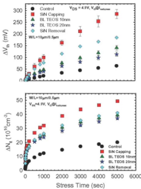
Fig. 7 shows thresholdvoltage shift (AVth) and increased interface statedensity(ANit) as afunction of thestresstime. The
SiN-capped sample depictstheworstdegradationinterms of the
largest shifts in these parameters, and the use ofTEOS buffer
layer apparently improves hot carrier degradation and the
BL-20nmTEOS sample shows the smallest degradations. We suspect that the bandgap narrowing effect, the increased carrier
mobility,andhydrogen speciesfrom the SiNcappingprocess [8] are the primary culprits for the aggravated hot carrier
degradations.Itis noted that the device withSiN-removaldepicts
much severe degradation over the control devices and devices
with TEOS bufferlayers,eventhoughthe channelstrain has been
....|.... |... |... |... |...
0 * ControlSiNCapping VDS=4.9V,VG@Isub. -A BLTEOS10nm 50 BLTEOS 20nm 00 * SiN Removal W/L=10pm/0.5trn 50 * 00 @@ * '. 50 t4 * * 0 n lit$ .... -... W/L=10m/0.5grn 50 VDS;=4.9V,VG@lsub,mav E 40* 30 j 20 *# * Control -j SiNCapping 10 N A BL TEOS1On * BL TEOS2On n- ...enya.. 0 1000 2000 3000 4000 5000 6000
Stress Time(sec)
Fig. 7 Results of hot-electron stressing at VDS=4.9V and maximum substrate current performed on all splits with channel width/length
lOlimA0.5pm. (a) Threshold voltage shift; (b) Interfacestategeneration.
CONCLUSION
Both the presence of the SiN capping layer and the
deposition process itselfexertsignificant impacts onthe device
operation and the associated reliability characteristics. The
accompanying bandgap narrowing, increased carriermobilityand
hydrogendiffusion from the SiNcappingprocesstendtoworsen
the hot-electron reliability. This work shows that, owing to the
use of hydrogen-containing precursors, abundant hydrogen
species is presumably incorporated in the oxide and may
contributetothe hot-electrondegradation,evenifthe SiNlayeris
removed later and the channelstrain is relieved.Furthermore, by blocking the diffusion of hydrogen species, the devices with
20nm-thick TEOS buffer layer can effectively improve the
hot-electron reliability without compromising the performance
enhancement by the strain induced by the SiN capping. Optimization of both the thickness of buffer layer and SiN
depositionprocessarethusessentialtotheimplementationof the
uniaxial straininNMOS devices.
ACKNOWLEDGMENTS
This workwas supported inpart bythe National Science Council of the Republic of China under contract No. NSC 95-2221 -E-009-297.
REFERENCES
[1]X. Chenetal., VLSI, 2006,pp.74-75.[2]M. Horstmannetal., IEDM, 2005,pp.233-236
[3]H. S. Momoseetal., IEDM, 1997,pp.452-456.
[4]A. Schwerinetal., ED-34, 1987,pp.2493-2500.
[5]M. V. Fischettietal., JAP-80, 1996,pp.2234-2252.
[6]N. Sanoetal., ED-42, 1995,pp.2211-2216.
[7] S. Deyetal., IRPS, 2006,pp.461-464.
[8]C. Y.Lu, SSDM, 2006,pp.528-529. 671 W/L=10[tm/0.5[tm VDS 4.9V Control SiNCapping N BLTEOS10nm BLTEOS 20nm SiN Removal