Fabrication of High Electrical Performance NILC-TFTs Using FSG Buffer Layer
C. C. Chena, Y.C. Wua, T. F. Tunga and H. Y. Wua, b
a Department of Materials Science and Engineering, National Chiao Tung University,
Hsinchu 30010, Taiwan, R.O.C
b National Nano Device Laboratory, Hsinchu 30010, Taiwan, R.O.C
Fluorinated-silicate-glass (FSG) was combined with Ni-metal-induced lateral crystallization (NILC) polycrystalline silicon thin-film transistors (poly-Si TFTs). It was found that the electrical performances were improved because the trap-state density was decreased by fluorine-ion passivation. Moreover, FSG-NILC-TFTs possess high immunity against the hot-carrier stress and, thereby, exhibit better reliability.
Introduction
Polycrystalline silicon thin-film transistors (poly-Si TFTs) have been widely used in active matrix organic liquid crystal displays (AMOLCDs) because their higher carrier mobility and lower threshold voltage than conventional amorphous thin-film transistors (a-Si TFTs) (1). Ni-metal-induced lateral crystallization (NILC) is one of these effective methods that can reduce the crystallization temperature to fabricate poly-Si TFTs on inexpensive glass substrates (2-3). However, in NILC, the poly-Si grain boundaries would trap Ni and NiSi2 precipitates which induce trap-state density increased, resulting
in threshold voltage shifting and lower field-effect mobility (4-5). In this letter, fluorine-ion was introduced to buffer oxide layer, subsequently deposited a-Si film and transformed the buffer layer to fluorinated-silicate-glass (FSG) layer at 550oC. Then the fluorine-ion would diffuse to the active layer and passivate the trap-state defect when NILC was carried out. The above phenomenon cause electrical characteristic enhancement (6-7). Moreover, the presence of Si-F bonds strengthens electrical endurance against hot-carrier impact.
Experiment
First, a 500-nm-thick SiO2 buffer layer was fabricated by thermal furnace. Then, the
fluorine-ion was implanted into the buffer oxide layer to form FSG layer. The projection
range of fluorine-ion was set at the middle of the FSG layerand the accelerating energy
was 30 keV. The dosage of fluorine ions was 2×1014 cm-2. Next, a 100-nm-thick undoped amorphous silicon layer was deposited by low pressure chemical vapor deposition (LPCVD) system on the FSG layers. The photoresist was patterned to form desired Ni lines, and a 5-nm-thick Ni film was deposited on the a-Si, subsequently annealed at 530oC for 48 h to form the NILC poly-Si film. To reduce Ni contamination, the unreacted Ni metal was removed by chemical etching. After the crystallization of the a-Si, the active regions were defined by RIE. The 100-nm-thcik TEOS oxide was deposited by plasma-enhanced CVD (PECVD) for gate oxide and 100-nm-thick poly-Si film was deposited by LPCVD for gate electrodes. P+-ion was implanted at a dose of 5×1015 cm−2 to form the source/drain and gate after defining the gate pattern by RIE etching. The
activation of the source/drain regions was realized by the thermal furnace under N2
ECS Transactions, 28 (1) 401-404 (2010) 10.1149/1.3375627 © The Electrochemical Society
401 ecsdl.org/site/terms_use) unless CC License in place (see abstract). address. Redistribution subject to ECS terms of use (see
140.113.38.11
ambient at 600oC for 24 h. For comparing the effect of fluorine-ion passivation, a typical NILC-TFT with SiO2 buffer layer was also fabricated.
Results and Discussions
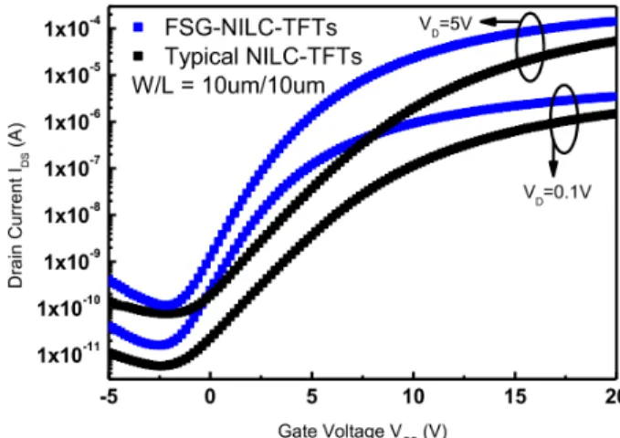
Fig. 1 show the ID–VG transfer characteristics of FSG-TFTs and typical
NILC-TFTs. The measured and extracted key device parameters are summarized in Table I. The performance of FSG-NILC-TFTs was far superior to that of typical NILC-TFTs. This implied when NILC was carried out; the fluorine-ion would diffuse to the active layer from FSG buffer layer, terminate dangling bonds, and replace the weak Si-H bonds in the grain boundaries and SiO2/poly-Si interface by forming stronger Si-F bonds (8-9). Fig. 2
show the secondary-ion mass spectroscopy (SIMS) analysis of FSG-NILC-TFTs of the fluorine, silicon, and oxygen atoms. It was found that the F-ion was piled up at the interface of FSG layer/poly-Si channel and poly-Si channel/gate oxide. The phenomenon indicated fluorine-ion effectively passivated the dangling bonds in the channel of FSG-NILC-TFTs, resulting in the trap-state density (NT) was reduced and improved electrical
properties (10). The trap state density, which could be extracted using Levinson and Proano’s method (11-12), was reduced from 4.6×1012 cm-2 to 3.1×1012 cm-2, as show in
Table I, leading to high field-effect mobility (μFE), low threshold voltage (VTH), low
subthreshold slope (S.S.) and high ON/OFF-current ratio (ION/IOFF) in FSG-NILC-TFTs.
Conclusions
An investigation of the effects of fluorine-ion passivation using the FSG buffer layer on the improvement of the electrical characteristics and reliability of NILC poly-Si TFTs has led to the development of a simple, effective process for improving the TFT electrical properties. The FSG-NILC-TFTs can be improved not only the transfer characteristics but also the electrical reliabilities. This result can be attributed to the fluorine-ion passivation effects and the weaker Si-H bonds and Si-Si bonds were replaced by stronger Si-F bonds.
Fig. 1 Transfer characteristics of FSG-NILC-TFTs and typical NILC-TFTs ECS Transactions, 28 (1) 401-404 (2010)
402 ecsdl.org/site/terms_use) unless CC License in place (see abstract). address. Redistribution subject to ECS terms of use (see
140.113.38.11
Fig. 2 The SIMS depth profile of FSG-NILC-TFTs of the fluorine, silicon, and oxygen atoms
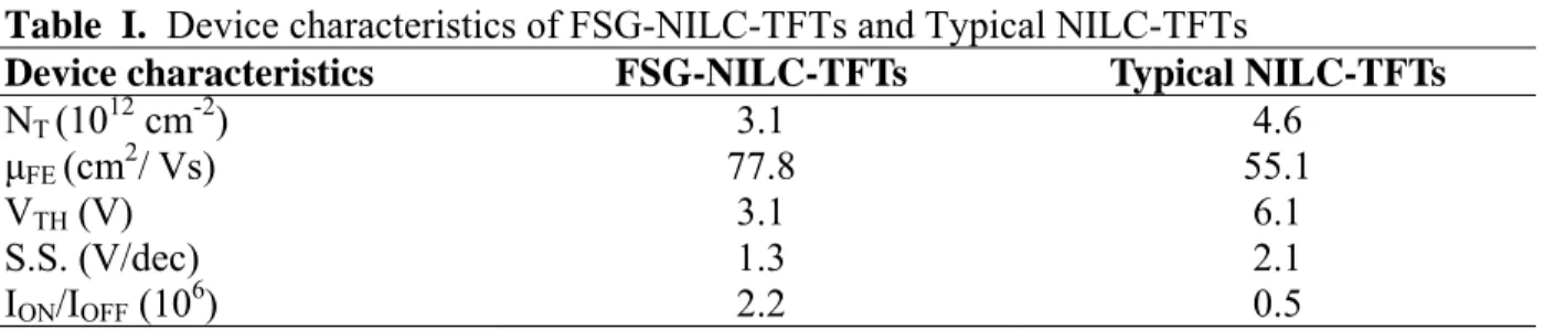
Table I. Device characteristics of FSG-NILC-TFTs and Typical NILC-TFTs
Device characteristics FSG-NILC-TFTs Typical NILC-TFTs
NT (1012 cm-2) 3.1 4.6 μFE (cm2/ Vs) 77.8 55.1 VTH (V) 3.1 6.1 S.S. (V/dec) 1.3 2.1 ION/IOFF (106) 2.2 0.5 Acknowledgments
This project was funded by Sino American Silicon Products Incorporation and the National Science Council of the Republic of China under Grant No. 95-2221-E009-087-MY3. Technical supports from the National Nano Device Laboratory, Center for Nano Science and Technology and the Nano Facility Center of the National Chiao Tung University are also acknowledged.
References
1. M. Stewart, R. S. Howell, L. Pires, and M. K. Hatalis, IEEE Trans. Electron
Devices, 48, 845 (2001)
2. S. W. Lee and S. K. Joo, IEEE Electron Device Lett., 17, 160 (1996).
3. Z. Meng, M. Wang, and M. Wong, IEEE Trans. Electron Devices, 47, 404 (2000) 4. P. J. van der Zaag, M. A. Verheijen, S. Y. Yoon, and N. D. Young, Appl. Phys.
Lett., 81, 3404 (2002).
5. G. A. Bhat, Z. Jin, H. S. Kwok, and M. Wong, IEEE Electron Device Lett., 20, 97 (1999)
6. C. H. Tu, T. C. Chang, P. T. Liu, C. Y. Yang, H. C. Liu, W. R. Chen, Y. C. Wu, and C. Y. Chang, IEEE Electron Devices Lett., 27, 262 (2006).
7. C. H. Tu, T. C. Chang, P. T. Liu, H. W. Zan, Y. H. Tai, C. Y. Yang, Y. C. Wu, H. C. Liu, W. R. Chen, and C. Y. Chang, Electrochem. Solid-State Lett., 8, G246 (2005).
ECS Transactions, 28 (1) 401-404 (2010)
403 ecsdl.org/site/terms_use) unless CC License in place (see abstract). address. Redistribution subject to ECS terms of use (see
140.113.38.11
8. C. H. Tu, T. C. Chang, P. T. Liu, C. Y. Yang, L. W. Feng, C. C. Tsai, L. T. Chang, Y. C. Wu, S. M. Sze, and C. Y. Chang, IEEE/OSA Journal of Display Technology,
3, 45 (2007).
9. S. D. Wang, T. Y. Chang, C. H. Chien, W. H. Lo, J. Y. Sang, J. W. Lee, and T. F. Lei, IEEE Electron Device Lett., 26, 467 (2005).
10. S. D. Wang, W. H. Lo, and T. F. Lei, J. Electrochem. Soc., 152, G703 (2005). 11. J. Levinson, G. Este, M. Rider, P. J. Scanlon, F. R. Shepherd, and W. D.
Westwood, J. Appl. Phys., 53, 1193 (1982).
12. R. E. Proano, R. S. Misage, and D. G. Ast, IEEE Tarns. Electron Devices, 36, 1915 (1989).
ECS Transactions, 28 (1) 401-404 (2010)
404 ecsdl.org/site/terms_use) unless CC License in place (see abstract). address. Redistribution subject to ECS terms of use (see
140.113.38.11