國 立 交 通 大 學
電子工程學系 電子研究所碩士班
碩
士
論
文
IEEE802.16e OFDMA 通道編
碼技術與數位訊號處理器實現之研究
Research in and DSP Implementation of Channel Coding
Techniques for IEEE 802.16e OFDMA
研 究 生:吳柏昇
指導教授:林大衛 博士
IEEE 802.16e OFDMA 通道編
碼技術與數位訊號處理器實現之研究
Research in and DSP Implementation of Channel Coding
Techniques for IEEE 802.16e OFDMA
研究生:吳柏昇
Student:
Po-Sheng
Wu
指導教授: 林大衛 博士 Advisor: Dr. David W. Lin
國 立 交 通 大 學
電子工程學系 電子研究所碩士班
碩士論文
A Thesis
Submitted to Department of Electronics Engineering & Institute of Electronics College of Electrical and Computer Engineering
National Chiao Tung University in Partial Fulfillment of the Requirements
for the Degree of Master of Science
in
Electronics Engineering June 2007
Hsinchu, Taiwan, Republic of China
IEEE 802.16e OFDMA 通道編
碼技術與數位訊號處理器實現之研究
研究生:吳柏昇 指導教授:林大衛 博士
國立交通大學
電子工程學系 電子研究所碩士班
摘要
IEEE 802.16e 無線通訊標準中,於系統的傳送端訂定了前向誤差改正編碼的機 制,藉此減低通訊頻道中雜訊失真的影響。通道編碼是本論文的重點。本篇論文前半部份重點在於,研究 IEEE 802.16e OFDMA 所訂定的迴旋編碼系統 並且實現在數位訊號處理器(DSP)上,針對 DSP 平台的特性以及迴旋編碼編碼的演算 法進行程式的改進。在論文中,我們將標準中制訂的四個必備的前向誤差改正編碼系 統,利用 C 語言驗證我們整個系統演算法上的正確性,在加成性白色高斯通道下模擬 了各種調變,模擬的結果增益比理論值大約有 1dB 的誤差,接著進一步以德州儀器公 司所發展的 TMS320C6416 DSP 為核心的平台上實現。經過在 DSP 平台上最佳化我們 的程式後,迴旋編碼的編碼器部份,於 DSP 模擬器上,可以到每秒 13793K 位元的處 理速度,而解碼器的部份可以達到每秒 805K 位元的處理速度。
本論文後半部份重點,研究 IEEE 802.16e OFDMA 所訂定的低密度奇偶校驗碼系 統並且實現在數位訊號處理器。研究低密度奇偶校驗碼傳統的編碼與解碼演算法,並 且介紹一些降低解碼複雜度的演算法。用 C 語言驗證系統演算法上的正確性,在加成 性白色高斯通道下模擬了各種調變與各種解碼演算法,並把模擬之結果與一些數學分 析的結果做比較。模擬的結果顯示降低複雜度的演算法和傳統的解碼表現相當接近。 接著從這些演算法中,根據運算複雜度,延遲時間,找出合適的演算法,實現在德州 儀器公司所發展的 DSP 平台上。經過在 DSP 平台上最佳化我們的程式後,編碼器部 份經過改進,可以到每秒 835K 位元的處理速度,而解碼器的部份僅可以達到每秒 4.7K 位元的處理速度。
Research in and DSP Implementation of Channel Coding
Techniques for IEEE 802.16e OFDMA
Student: Po-Sheng Wu Advisor: Dr. David W. Lin
Department of Electronics Engineering
& Institute of Electronics
National Chiao Tung University
Abstract
In the IEEE 802.16e wireless communication standard, a Forward Error Correction (FEC) mechanism is presented at the transmitter side to reduce the noisy channel effect. The focus is on the channel coding.
The focus of the fist part of this thesis is the research of the convolutional code defined in IEEE 802.16e OFDMA standard and modifying FEC algorithms to match the architecture of DSP platform. We have implemented four required FEC schemes defined in the standard on the C program to insure the correctness of our algorithm. We simulate the different modulation in AWGN channel and the coding gain is almost achieve theoretic values. Then we implement the project on the Texas Instruments digital signal processor (DSP). After optimizing the programs on the DSP platform, the improved FEC encoder can achieve a data processing rate of 13793 kbps and the improved FEC decoder can achieve a processing rate of 805 kbps on the TI TMS320C6416 DSP simulator.
The focus of second part is the low-density parity-check (LDPC) code defined in IEEE 802.16e OFDMA. We explain the conventional encoding and decoding algorithm, and some reduced-complexity decoding algorithms. We simulate the LDPC code for different modulation and decoding algorithms in AWGN and compare the simulation results with analytical results. Simulation results show that these reduced-complexity decoding algorithms for LDPC codes achieve a performance very close to that of conventional algorithm. According to computational complexity and latency, we choose the adaptable algorithm and implement on DSP. After optimizing the programs on the DSP platform, the improved encoder can achieve a data processing rate of 835 kbps and the improved decoder can achieve a processing rate of 4.7 kbps on the TI C6416 DSP simulator.
誌謝
本篇論文的完成,誠摯地感謝我的指導老師 林大衛 博士,從踏入交通大學 電子所開始,多虧老師的循循善誘,不但給予我在課業、研究上的幫助,使我學 到了分析問題及解決問題的能力。同時老師樂觀的生活態度也影響了我,讓我更 有勇氣面對各種困難。在此,僅向老師及老師的家人致上最高的感謝之意。 另外要感謝的,是實驗室的洪崑健學長和吳俊榮學長。謝謝你們熱心地幫我 解決了許多通訊方面相關的疑問。 感謝通訊電子與訊號處理實驗室(commlab),提供了充足的軟硬體資源,讓 我在研究中不虞匱乏。感謝 93 級國偉、治傑、勇竹三位學長的指導,以及 94 級介遠、志岡、政達、耀鈞、順成、凱庭、錫祺、浩廷、育成、耀仚等實驗室成 員,平日和我一起唸書,一起討論,也一起打混,讓我的研究生涯充滿歡樂又有 所成長。期待大家畢業之後都能有不錯的發展。 最後,要感謝的是我的家人,他們的支持讓我能夠心無旁騖的從事研究工作。 謝謝所有幫助過我、陪我走過這一段歲月的師長、同儕與家人。謝謝! 誌於 2007.6 風城交大 柏昇Contents
1 Introduction 1
1.1 Scope of the Work . . . 1
1.2 Organization of This Thesis . . . 2
2 FEC in IEEE 802.16e OFDMA and Associated Decoding methods 3 2.1 Convolutional Code Specifications [1] . . . 3
2.1.1 Randomizer [1] . . . 5
2.1.2 Convolutional Encoder [1] . . . 6
2.1.3 Interleaver [1] . . . 8
2.1.4 Modulation [1] . . . 10
2.2 Decoding Under Convolutional Encoding . . . 10
2.2.1 Demodulation Under Bit-Interleaved Coded Modulation . . . 11
2.2.2 De-Interleaver . . . 14
2.2.3 Tail-Biting Convolutional Decoding . . . 15
2.3 LDPC Code Specifications . . . 16
2.3.2 LDPC Code in IEEE 802.16e OFDMA [1] . . . 20
2.4 Decoding of LDPC code . . . 21
2.4.1 The Belief Propagation Decoding Algorithm [17] . . . 21
2.4.2 Some Reduced-Complexity LDPC Decoding Algorithms . . . 24
3 DSP Implementation Environment 28 3.1 The DSP Baseboard (SMT395) . . . 28
3.2 The DSP Chip . . . 29
3.2.1 Central Processing Unit [23] . . . 32
3.2.2 Memory [24] . . . 37
3.3 TI’s Code Development Environment [25], [26] . . . 39
3.4 Code Development Flow [27] . . . 41
3.5 Acceleration Rules . . . 43
3.5.1 Compiler Optimization Options [27] . . . 43
3.5.2 Fixed–Point Coding . . . 45
3.5.3 Loop Unrolling . . . 45
3.5.4 Packet Data Processing . . . 46
3.5.5 Register and Memory Arrangement . . . 47
3.5.6 Software Pipelining . . . 47
3.5.7 Macros and Intrinsic Functions . . . 48
4 Simulation and DSP Implementation of Convolutional Encoder and
De-coder 49
4.1 Coding Gain Analysis . . . 49
4.2 Performance in AWGN with Floating-Point Processing . . . 52
4.3 Performance in AWGN with Fixed-Point Processing . . . 55
4.4 Implementation on DSP . . . 61
4.4.1 Profile of the DSP code . . . 62
5 Simulation and DSP Implementation of LDPC Encoder and Decoder 71 5.1 Performance in AWGN Channel with Floating-Point Processing . . . 71
5.1.1 Number of Iterations . . . 71
5.1.2 Performance at Different Codeword Lengths . . . 72
5.1.3 Performance with Different Modulations . . . 72
5.1.4 Performance at Different Coding Rates . . . 74
5.1.5 Performance of Reduced-Complexity Algorithm . . . 76
5.2 Performance in AWGN Channel with Fixed-Point Processing . . . 77
5.2.1 Profile of the DSP code . . . 81
6 Conclusion and Future Work 92
List of Figures
2.1 Convolutional coding structure in transmitter (top path) and decoding in
receiver (bottom path). . . 4
2.2 PRBS for data randomization (from [1]). . . 5
2.3 Convolutional encoder of rate 1/2 (from [1]). . . . 6
2.4 The second permutation of interleaver. . . 9
2.5 QPSK, 16-QAM, and 64-QAM constellations (from [1]). . . 10
2.6 Metric partitions of the 16-QAM constellation (from [9]). . . 14
2.7 Trellis for tail-biting convolutional decoding (from [2]). . . 16
2.8 LDPC coding structure in transmitter (top path) and decoding in receiver (bottom path). . . 17
2.9 Tanner graph of a parity check matrix . . . 19
2.10 Base model of the rate-1/2 code (from [1]). . . . 21
2.11 Base model of the rate-2/3, type A code (from [1]). . . . 21
2.12 Base model of the rate-2/3, type B code (from [1]). . . . 22
2.13 Base model of the rate-3/4, type A code (from [1]). . . . 22
2.15 Base model of the rate-5/6 code (from [1]). . . . 22
2.16 Fast decaying function f (x) = logex+1 ex−1. . . 25
3.1 SMT395 Module. . . 29
3.2 Block diagram of TMS320C6416 DSP (from [23]). . . 31
3.3 The TMS320C64x DSP chip architecture and comparison with earlier TMS320C62x/C67x chip (from [23]). . . 33
3.4 Pipeline phases of TMS320C6416 DSP (from [23]). . . 34
3.5 Execution stage length description for each instruction type (from [23]). . . . 35
3.6 TMS320C64x CPU data paths (from [23]). . . 38
3.7 C64x cache memory architecture (from [24]). . . 39
3.8 Code development flow for TI C6000 DSP (from [27]). . . 42
3.9 Loop unrolling. . . 46
3.10 The block diagram of SIMD. . . 47
3.11 Software-pipelined loop. . . 48
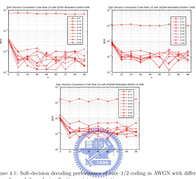
4.1 Soft-decision decoding performance of rate–1/2 coding in AWGN with differ-ent value of α and β employing floating-point computation. . . . 53
4.2 oft-decision decoding performance of rate–2/3 and rate–3/4 coding in AWGN with different value of α and β employing floating-point computation. . . . . 54
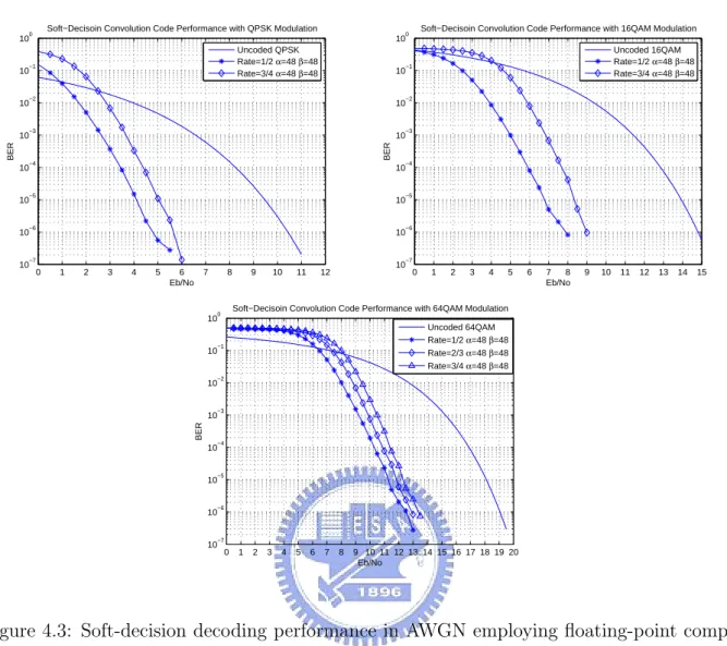
4.3 Soft-decision decoding performance in AWGN employing floating-point com-putation with α = β = 48. . . . 55 4.4 Soft-decision decoding performance in AWGN with different input precisions. 57
4.5 Soft-decision decoding performance employing fixed-point computation in AWGN
with different value α and β. . . . 58
4.6 Soft-decision decoding performance in AWGN with α = 48 and β = 48 em-ploying fixed-point computation. . . 59
4.7 Comparison between soft-decision decoding performance in AWGN using floating-point computation and that using fixed-floating-point computation. . . 60
4.8 The C code of Viterbi decoder. . . 63
4.9 The assembly code of Viterbi decoder (1/5). . . 64
4.10 The assembly code of Viterbi decoder (2/5). . . 65
4.11 The assembly code of Viterbi decoder (3/5). . . 66
4.12 The assembly code of Viterbi decoder (4/5). . . 67
4.13 The assembly code of Viterbi decoder (5/5). . . 68
4.14 Software pipeline information for Viterbi decoder. . . 69
5.1 LDPC decoding performance in different iteration numbers with floating-point computation. . . 72
5.2 LDPC decoding performance in different codeword length with floating-point computation. . . 73
5.3 LDPC decoding performance with different modulation employing floating-point computation. . . 73
5.4 LDPC Decoding Performance in Different Coding Rate (floating-point). . . . 75
5.5 LDPC decoding performance using different decoding algorithm employing floating-point computation. . . 76
5.6 LDPC decoding performance at different bit numbers with different
modula-tions employing fixed-point computation. . . 78
5.7 LDPC decoding performance at different bit numbers at two different coding rate employing fixed-point computation. . . 79
5.8 LDPC decoding performance at different bit numbers at two different code-word lengths employing fixed-point computation. . . 80
5.9 The C codes of circular shift. . . 83
5.10 The assembly codes of circular shift (1/2). . . 84
5.11 The assembly codes of circular shift (2/2). . . 85
5.12 The C code of computing form check nodes to bit nodes. . . 86
5.13 The assembly code of computing form check nodes to bit nodes (1/3). . . 88
5.14 The assembly code of computing form check nodes to bit nodes (2/3). . . 89
5.15 The assembly code of computing form check nodes to bit nodes (3/3). . . 90
List of Tables
2.1 Mandatory Channel Coding Schemes for Each Modulation Method . . . 4
2.2 The Convolutional Code with Puncturing Configuration . . . 7
2.3 Bit Interleaved Block Sizes and Modulos . . . 9
2.4 Bit Metric for Method-ML and Method-LLR . . . 13
2.5 Comparison of Main Operations of Different Decoding Algorithms . . . 27
3.1 Functional Units and Operations Performed (from [23]) . . . 36
3.2 Sizes of Different Data Types . . . 45
3.3 Comparison Between Unrolled and not Unrolled . . . 46
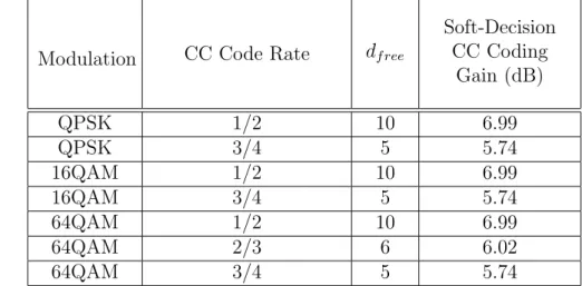
4.1 Coding Gain Upper-Bound in AWGN at BER = 10−6 . . . . 51
4.2 Approximate Coding Gain Based on Analysis of Minimum Codeword Distance 52 4.3 Comparison of Convolutional Coding Gain froms in AWGN at BER = 10−6 56 4.4 Soft-Decision Decoding Performance with α = 48 and β = 48, in AWGN at BER = 10−6 Employing Fixed-Point Computation . . . . 61
4.5 Final Profile of Convolution Code (Cycles) . . . 69
4.7 Final Profile of Convolution Code (Code Size) . . . 70
5.1 Comparison of Coding Gain Between LDPC Codes and Convolutional Codes at Code Rate 1/2 in AWGN at BER = 10−6 . . . . 74
5.2 Threshold for Each Code Rate under BPSK Modulation in AWGN Channel [20]. . . 75
5.3 LDPC Coding Gain between Floating-point and Fixed-point in AWGN at BER = 10−5. . . . 77
5.4 Original Profile of LDPC Encoder (Cycles) . . . 82
5.5 Profile of LDPC Encoder with Matrix Table (Cycles) . . . 82
5.6 Profile of LDPC Encoder with Different Coding Rates . . . 82
5.7 Profile of LDPC Decoder with different Coding Rate . . . 83
Chapter 1
Introduction
1.1
Scope of the Work
Digital wireless transmission is a trend in the next generation of consumer electronics. Due to this demand high data transmission rate and mobility are needed. The OFDM modulation technique for wireless communication has been a main stream in recent years. IEEE has completed several standards, including the IEEE 802.11 series for LANs (local area networks) and IEEE 802.16 series for MANs (metropolitan area networks), based on OFDM technique. Our study is based on the IEEE 802.16e standard, which specifies the air interface of mobile broadband wireless multiple access systems providing multiple access.
In wireless communication, the transmitted signals are easily interfered and distorted by variance things sources such as the crowd traffic, bad weather, the obstacle of buildings, etc. Digital wireless transmission with multimedia contents such as audio and video is a trend. These services often exhibit high data rates and require high quality reproduction. To improve the robustness of the wireless communication against the noisy channel condition, the FEC (forward-error-correcting coding) mechanism is a must in almost every commercial communication standard, including the IEEE 802.16e.
convolutional coding. In addition, bit interleaver and M-ary QAM modulation are used after coding. We also discuss the LDPC code in IEEE 802.16e for OFDMA.
In this thesis, we focus on the study of the simulation and the DSP implementation of the FEC schemes of the IEEE 802.16e standard. We first review the FEC methods used in IEEE 802.16e and study the encoding and decoding techniques. Then we perform computer simulation to investigate the coding performance. Finally, we implement the FEC algorithms on DSP with fixed-point computation. We also seek to optimize the DSP program for efficient execution.
1.2
Organization of This Thesis
This thesis is organized as follows.
• Chapter 2 introduces the convolutional code and the LDPC code of IEEE 802.16e. • Chapter 3 describes the DSP implementation environment.
• Chapter 4 discusses simulation and the DSP implementation of the convolution code. • Chapter 5 discusses simulation and the DSP implementation of the LDPC code. • Chapter 6 contains the conclusion and points out some future work.
Chapter 2
FEC in IEEE 802.16e OFDMA and
Associated Decoding methods
The channel coding schemes usually used in IEEE 802.16e is tail-biting convolutional code. Block turbo code, convolutional turbo code, zero tailed convolutional code and LDPC code are the options.
2.1
Convolutional Code Specifications [1]
The contents of this section have been taken a large extent from [2].
The mandatory channel coding scheme used in IEEE 802.16e OFDMA is as shown in Fig. 2.1. Input data streams are divided by the randomizer to clean up the bit correlation, and then each data block is encoded by the convolutional encoder. The block-by-block coding makes the convolutional code effectively a block code.
Between the convolutional coder and the modulator is a bit interleaver, which protects the convolutional code from severe impact of burst errors and increases overall coding per-formance. This approach has been termed “bit-interleaved coded modulation (BICM)” in the literature [3].
Figure 2.1: Convolutional coding structure in transmitter (top path) and decoding in receiver (bottom path).
Table 2.1: Mandatory Channel Coding Schemes for Each Modulation Method Modulation Uncoded Block Size (bytes) Overall Code Rate Coded Block Size (bytes) Number of Used Sub-channels QPSK 6 1/2 12 1 QPSK 12 1/2 24 2 QPSK 18 1/2 36 3 QPSK 24 1/2 48 4 QPSK 30 1/2 60 5 QPSK 36 1/2 72 6 QPSK 9 3/4 12 1 QPSK 18 3/4 24 2 QPSK 27 3/4 36 3 QPSK 36 3/4 48 4 16QAM 12 1/2 24 1 16QAM 24 1/2 48 2 16QAM 36 1/2 72 3 16QAM 18 3/4 24 1 16QAM 36 3/4 48 2 64QAM 18 1/2 36 1 64QAM 36 1/2 72 2 64QAM 24 2/3 36 1 64QAM 27 3/4 36 1
Figure 2.2: PRBS for data randomization (from [1]).
To make the system more flexibly adaptable to the channel condition, nineteen coding-modulation schemes are defined in IEEE 802.16e, as shown in Table 2.1. The different coding rates are made by puncturing of the native convolutional code. The puncturing mechanism in convolutional coding can provide variable code rates through one convolutional encoder.
2.1.1
Randomizer [1]
The randomizer is a pseudo random binary sequence (PRBS) generator, as depicted in Fig. 2.2. If the amount of data to transmit does not fit exactly the amount of data allocated, padding of 0xFF (“1” only) shall be added to the end of the transmission block, up to the amount of data allocated. The shift-register of the randomizer shall be initialized for every 1250 bytes passed through (if the allocation is larger then 1250 bytes).
The randomizer sequence is applied only to information bits. Preambles are not random-ized.
Both in the uplink and downlink, the randomizer shall be re-initialized at the start of each frame with the sequence
Figure 2.3: Convolutional encoder of rate 1/2 (from [1]).
2.1.2
Convolutional Encoder [1]
Each block is encoded by a binary convolutional encoder, which has native rate 1/2 and constraint length 7. The generator polynomials for the two output bits are 171OCT and
133OCT, respectively. The generator is depicted in Fig. 2.3.
The coded bits may be punctured to allow different rates, which is known as rate-compatible punctured convolutional coding (RCPC). Furthermore, tail-biting is performed, by initializing the encoder’s memory with the last data bits of the block. The encoding algo-rithm and the decoding algoalgo-rithm (based on Viterbi decoder) for the RCPC with tail-biting convolutional are discussed late.
Punctured Convolutional Code
Puncturing patterns and serialization order of the convolutional code in IEEE 802.16e are as defined in Table 2.2. In this table, “1” means a transmitted bit and “0” a removed bit, whereas X and Y are in reference to Fig. 2.3. Note that the Dfree after puncturing is lower than that of the native convolutional code at rate 1/2, which is equal to 10 [7, Chapter 8].
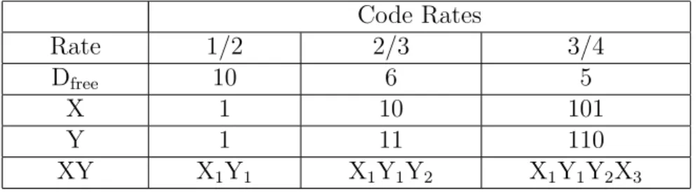
Table 2.2: The Convolutional Code with Puncturing Configuration Code Rates Rate 1/2 2/3 3/4 Dfree 10 6 5 X 1 10 101 Y 1 11 110 XY X1Y1 X1Y1Y2 X1Y1Y2X3 Tail-Biting
The convolutional code in IEEE 802.16e is terminated in a block, and thus becomes a block code. In general, there are three methods to achieve code termination[4]. For ease of understanding, we describe these methods in terms of a binary (n, k, m) convolutional code (of rate k/n and register length m) for an information sequence length of L bits.
• Direct truncation. The codeword is produced by inputting into the encoder (initialized
with all zeros) L information bits, so the codeword length is nL/k. However, this code has the disadvantage that there is little error protection ability afforded to the last information bits.
• Zero tail. The codeword is produced by inputting into the encoder (initialized with
all zeros) L information bits followed by m zeros (tail bits), so the codeword length is
n(L + m)/k. However, this code has the disadvantage of rate loss of m/(L + m) since
the effective rate is (k/n)(L/(L + m)) = (k/n)(1 − m/(L + m)).
• Tail biting. We first initialize the encoder with the last m information bits, and then
inputting into the encoder L information bits to produce codeword whose length is
nL/k. This code has the disadvantage of complex Viterbi decoder since the starting
IEEE 802.16e uses the tail-biting approach, which has better performance compared with direct-truncation convolutional code and does not lose rate compared with zero-tail convolutional code. However, we pay the price of a complex decoder. The optimal decoder of tail-biting convolutional code, as suggested in [4], is to run M parallel Viterbi decoders, where
M = 2m is the number of states in the trellis. Each Viterbi decoder postulates a different
starting and ending state. The Viterbi decoder that produces the globally best metric gives the maximum likelihood estimate of the transmitted bits. The obvious disadvantage of this method is the M times complexity compared to decoding for the code with zero tail bits. Therefore, we consider a suboptimal decoder which can reduce the complexity to less than 2 times the normal Viterbi algorithm. This decoder combines the algorithms proposed in [5] and [6]. We introduce it later.
Another interesting property is the error rates at different positions in the codeword, which are analyzed in [5] and [6]. In zero-tail convolutional code, there is lower error rate in the first and the last information bits because the decoder knows the starting and ending states in the trellis. In tail-biting convolutional code, if the suboptimal decoder is adopted, there is almost equal error rate through the codeword when the parameters used in the decoder are proper.
2.1.3
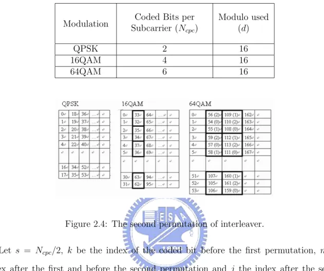
Interleaver [1]
The encoded data bits are interleaved by a block interleaver with a block size corresponding to the number of coded bits per the specified allocation, Ncbps (see Table 2.3). The
inter-leaver is defined by a two-step permutation. The first ensures that adjacent coded bits are mapped onto non-adjacent carriers. The second insures that adjacent coded bits are mapped alternately onto less or more significant bits of the constellation, thus avoiding long runs of lowly reliable bits.
Table 2.3: Bit Interleaved Block Sizes and Modulos
Modulation Subcarrier (NCoded Bits per
cpc) Modulo used (d) QPSK 2 16 16QAM 4 16 64QAM 6 16
Figure 2.4: The second permutation of interleaver.
Let s = Ncpc/2, k be the index of the coded bit before the first permutation, m the
index after the first and before the second permutation and j the index after the second permutation, just prior to modulation mapping. The first permutation is defined by
m = (Ncbps
d ) · kmod(d)+ f loor( k
d), k = 0, 1, · · · , Ncbps− 1, (2.1)
and the second permutation is defined by
j = s · f loor(m
s ) + (m + Ncbps− f loor( d · m Ncbps
))mod(s), m = 0, 1, · · · , Ncbps− 1. (2.2)
The first permutation is a block interleaving. And in Fig. 2.4, we show the second permutation after the block interleaving.
Figure 2.5: QPSK, 16-QAM, and 64-QAM constellations (from [1]).
2.1.4
Modulation [1]
After bit interleaving, the data bits are entered serially to the constellation mapper. Gray-mapped QPSK and 16-QAM are supported, whereas the support of 64-QAM is optional. The constellations as shown in Fig. 2.5 shall be normalized by multiplying the constellation points with the indicated factor c to achieve equal average power. The constellation-mapped data shall be subsequently modulated onto the allocated data carriers.
2.2
Decoding Under Convolutional Encoding
For Viterbi decoder, there are two decision types: decision and soft-decision. If hard-decision is adopted, the metric used in Viterbi decoding is the Hamming distance, which counts the bit errors, between each trellis path and the hard-limited output of the demodu-lator to find the path with least errors. However, the coding gain will lose 2 to 3 dB compared to soft-decision decoding [7, Chapter 8]. Hence soft-decision is adopted in our study.
For optimal soft-decision Viterbi decoding in AWGN channel, the metric should be the Euclidean distance between each trellis path and the soft-output of the demodulator. The problem now is that there is a bit interleaver between the convolutional encoder and the modulator in the transmitter. Therefore, the optimal decoder should be based on the super-trellis combining the convolutional code, the interleaver, and the QAM modulator, but this is too complex to be practical. Indeed, the puncturing mechanism adds further complexity to the super-trellis structure. Thus, we consider a suboptimal decoder based on bit-by-bit metric computation, which is proposed in [3], [8], and [9].
2.2.1
Demodulation Under Bit-Interleaved Coded Modulation
Let a[i] = aI[i] + jaQ[i] denote the QAM symbol transmitted in the ith sub-carrier of
OFDMA symbol and {bI,1, · · · , bI,k, · · · , bI,t, bQ,1, · · · , bQ,k, · · · , bQ,t} be the corresponding
bit sequence. Assuming that the ISI (inter–OFDMA symbol interference) and ICI (inter– channel interference) are completely eliminated, then the received signal of the sub-carrier can be written as
r[i] = Gch[i] · a[i] + w[i], (2.3)
where Gch[i] is the channel frequency response complex coefficient for the ith sub-carrier and w[i] is the complex additive white Gaussian noise (AWGN) with variance σ2 = N
0. If the channel estimate is error free, the output of the one-tap equalizer is given by
y[i] = a[i] + w[i]/Gch[i] = a[i] + w0[i], (2.4)
where w0[i] is still complex AWGN noise with variance σ02(i) = σ2/|G
ch[i]|2.
According to the MAPSE (maximum a posterior sequence estimation) criterion, the following maximization should be performed to estimate the encoded bit sequence b:
ˆ
b = arg max
where r is the received sequence of QAM signals. Assume that the transmitted symbols are equally distributed. Then the MAPSE criterion can be replaced by the ML (maximum likelihood) criterion as:
ˆ
b = arg max
b P [r|b]. (2.6) We further assume that Gch[i] is known to the receiver and that the transmitted bits are
i.i.d.
For each in-phase or quadrature bit (i.e., bI,k or bQ,k), two metrics can be derived
corre-sponding to the two possible values 0 and 1,respectively. For bit bI,k, first the QAM
constel-lation is split into two partitions of complex symbols, namely SI,k(0) comprising the symbols with a “0” in position (I, k) and SI,k(1), which is complementary. Then the two metrics are obtained by
m0c(bI,k) =
X
α∈SI,k(c)
log p(r[i]|a[i] = α) ≈ max
α∈S(c)I,k
log p(r[i]|a[i] = α), c = 0, 1. (2.7) Since the conditional pdf of r[i] is complex Gaussian as
p(r[i]|a[i] = α) = √1 2πσ exp{− 1 2 |r[i] − Gch[i]α|2 σ2 } (2.8)
and r[i] = Gch[i] · y[i], the metrics defined in (2.7) are equivalent to mc(bI,k) = |Gch[i]|2· min
α∈SI,k(c)
|y[i] − α|2. (2.9) Finally, these metrics are de-interleaved, i.e., each couple (m0, m1) is assigned to the bit position in the decoded sequence according to the de-interleaver map, and fed to the Viterbi decoder which selects the binary sequence with the smallest cumulative sum of metrics. We name this method Method-ML in the following discussion.
Table 2.4: Bit Metric for Method-ML and Method-LLR
Method-ML Method-LLR
Bit metric (decided “0”) m0 [14(m0− m1) + 1)]2 Bit metric (decided “1”) m1 [14(m0− m1) − 1)]2
in [9] to reduce the complexity of Method-ML. It defines LLR(bI,k) as LLR(bI,k) , |Gch[i]|2 4 { minα∈S(0) I,k |y[i] − α|2− min α∈SI,k(1) |y[i] − α|2} , (m0(bI,k) − m1(bI,k))/4 , |Gch[i]|2· DI,k. (2.10)
The quadrature part is similarly defined. The metrics sent to the Viterbi decoder of the two methods are defined in Table 2.4. Note that the difference between the bit metrics for the decided “0” and “1” is the same for the two methods, namely ±(m0− m1). Thus the decoded bit sequence will be the same for the two methods.
In Method-LLR, only (m0− m1)/4 is sent to the de-interleaver while in Method-ML, both
m0 and m1 are sent. Besides, we can reduce (m0− m1)/4 = |Gch[i]|2· DI,k to a simple form
constituting of yI[i] itself because Gray-coding is used in the constellation map of M-ary
QAM modulation in IEEE 802.16e.
Figure. 2.6 shows the partitions (SI,k(0), SI,k(1)) for the generic bit bI,k in the case of the
16-QAM constellation. As a consequence,
DI,k = 1 4{ minα∈S(0) I,k |y[i] − α|2− min α∈SI,k(1) |y[i] − α|2} can be simplified as follows.
DI,1 =
−yI[i], |yI(i)| ≤ 2 −2(yI[i] − 1), yI(i) > 2 −2(yI[i] + 1), yI(i) < 2
∼= −yI[i], (2.11)
SI,10 SI,11 S1 S1 I,2 S0 I,2 I,2 x x −1 1 3 −3 (10) (00) (01) I −1 1 3 −3(11) (10) (00) (01) (11) BI,1 BI,2 Q Q I
Figure 2.6: Metric partitions of the 16-QAM constellation (from [9]). The same observation holds for QPSK and 64-QAM constellations.
For QPSK, DI = −yI[i]. For 64-QAM,
DI,1 =
−yI[i], |yI[i]| ≤ 2 −2(yI[i] − 1), 2 < yI[i] ≤ 4 −3(yI[i] − 2), 4 < yI[i] ≤ 6 −4(yI[i] − 3), yI[i] > 6
−2(yI[i] + 1), −4 ≤ yI[i] < −2 −3(yI[i] + 2), −6 ≤ yI[i] < −4 −4(yI[i] + 3), yI[i] < −6
∼ = −yI[i], (2.13) DI,2 =
2(|yI[i]| − 3), |yI[i]| ≤ 2 −4 + |yI[i]|, 2 < |yI[i]| ≤ 6
2(|yI[i]| − 5), |yI[i]| > 6
∼= −4 + |yI[i]|, (2.14)
DI,3 =
½
−|yI[i]| + 2, |yI[i]| ≤ 4 |yI[i]| − 6, |yI[i]| > 4
¾
= ||yI[i]| − 4| − 2. (2.15)
2.2.2
De-Interleaver
The de-interleaver, as the interleaver, is also defined by two permutations. Let j be the index of the received bit before the first permutation, m be the index after the first and before the second permutation, and k be the index after the second permutation, just prior to delivering the coded bits to the convolutional decoder. The first permutation is defined
by the rule m = s · f loor(j s) + (j + f loor( d · j Ncbps ))mod(s), j = 0, 1, · · · , Ncbps− 1, (2.16)
and the second permutation is defined by the rule
k = d · m − (Ncbps− 1) · f loor( d · m Ncbps
), m = 0, 1, · · · , Ncbps− 1. (2.17)
Note that the quantity sent to the decoder are the bit metrics from the demodulator.
2.2.3
Tail-Biting Convolutional Decoding
We first extend the received sequence by repeating the first (α +β)(n/k) received bits, where
α and β are two important parameters that we have to set. In the Viterbi decoder, the trellis
is initialized by making all states equally likely, and the Viterbi algorithm is executed for the extended received sequence. A traceback is performed from the best state at the end of the extended received sequence, and a portion of the data in the decoded block, from position
α on for the length of information bits, is chosen as the estimate of the data block.
This scheme relies on the fact that if the received sequence is circularly repeated, the trellis of the extended received sequence can be considered circular since tail-biting code starts and ends in the same state. The trellis of the tail-biting convolutional decoder is depicted in Fig. 2.7. Because the starting state is unknown, the first α surviving paths of the decoder may not be the correct paths. Only after enough depth can the surviving paths approach the correct ones. Thus the later part of the decoded block will be more likely to be the correct information data.
Another issue that should be considered is the traceback mechanism. The surviving path will be almost unique after some depth into the trellis. Therefore, the trellis can be truncated and the traceback mechanism performed after some delay, say τ . A smaller τ entails shorter
circularly repeat Length α Lengthβ S0 S1 SP SM SM−1 S0 S1 SP SM SM−1 S0 S1 SP SM SM−1 correct path
incorrect path surviving paths non−unique Repeat Length Information Length (L)
Length L (the valid decoded bits)
(α+β)
Figure 2.7: Trellis for tail-biting convolutional decoding (from [2]).
decoding delay and smaller amount of memory requirement. To avoid multiple tracebacks our Viterbi decoder does traceback only at the end of the extended received sequence, and the performance will be a little better than the one with truncation since the decision depth is much longer than τ for the earlier bit. For the value of τ , a conventional value is 5 times the register length [10].
Since the ending state of the trellis for the extended received data is unknown and the decision depths for the latest decoded data are not long enough to make the surviving paths unique, the latest decoded data will not be reliable and can not be as used the decoded data. The unreliable data length is set to β, which should be related (actually equal) to τ . We have used simulation results to decide the values of α and β.
2.3
LDPC Code Specifications
The low–density parity check (LDPC) coding scheme used in IEEE 802.16e OFDMA is shown in Fig. 2.8. The randomized input data are first encoded by the LDPC encoder.
Figure 2.8: LDPC coding structure in transmitter (top path) and decoding in receiver (bot-tom path).
The encoder and then interleaved by the bit interleaver. Likewise, there are three different modulation types.
LDPC codes are a special case of error correcting codes that have recently been receiving received much attention because of their very high throughput and very good decoding performance. Inherent parallelism in the message passing decoding algorithm for LDPC codes makes them very suitable for hardware implementation. The LDPC codes can be used in any digital environment that high data rate and strong error correction ability are important.
Gallager [11] proposed LDPC codes in the early 1960s, but his work received little atten-tion until after the invenatten-tion of turbo codes in 1993, which used the same concept of iterative decoding. In 1996, MacKay and Neal [12], [13] re-discovered LDPC codes. Chung et al. [14] showed that a rate-1/2 LDPC code with block length of 107 in binary input AWGN can achieve a threshold of just 0.0045 dB away from the Shannon limit.
LDPC codes have several advantages over turbo codes. First, the sum-product decoding algorithm for these codes has inherent parallelism that can be exploited to achieve a greater speed of decoding. Second, unlike turbo codes, decoding error is a detectable event which results in a more reliable system. Third, very low complexity decoders, such as the modified minimum-sum algorithm that closely approximate the sum-product in performance, can be designed for these codes.
Our interest is in both low algorithm complexity and high decoding speed, as these are both desirable under the IEEE 802.16e applications.
Complexity in iterative decoding can be divided into two types: first, complexity of the computations in each iteration and second, the number iterations. Naturally, there is a trade-off between the decoding performance and the complexity and decoding speed.
In this section, we will only discuss the LDPC encoder and decoder block. Other blocks in Fig. 2.8 are the same as in previous section.
2.3.1
Overview of LDPC Code
LDPC codes are a class of linear block codes corresponding to a sparse parity check matrix
H. The term “low-density” means that the number of 1s in each row or column of H is
small compared to the block length n. In other words, the density of 1s in the parity check matrix which consists of only 0s and 1s is very low and sparse. Given k information bits, the set of LDPC codewords c in the code space C of length n spans the null space of the parity check matrix H, i.e., cHT = 0.
For a (Wc, Wr) LDPC code, each column of the parity check matrix H has Wc ones and
each row has Wr ones; this is called a regular code and Wc and Wr are tenoned the column
degree and the row degree, respectively. The degrees per row or column are not constant, then the code is irregular. Some of the irregular codes have shown better performance than regular ones. But irregularity results in more complex hardware and inefficiency in terms of re-usability of functional units. The IEEE 802.16e standard uses irregular codes. Moreover, the codes in 802.16e are systematic, which means that n − k redundant bits are added to k bits of message to form an n bits codeword.
LDPC codes can be represented effectively by a bipartite graph called a Tanner graph [15], [16]. A bi-partite graph is a graph (nodes or vertices are connected by undirected edges)
Figure 2.9: Tanner graph of a parity check matrix
whose nodes may be separated into two classes and where edges may only be connecting two nodes not residing in the same class. The two classes of nodes in a Tanner graph are bit nodes (or variable nodes) and check nodes. The Tanner graph of a code is drawn according to the following rule: Check node fj , j = 1, · · · , n − k, is connected to bit node xi, i = 1, · · · , n,
whenever element hji in H (parity check matrix) is a one. Figure 2.9 shows a Tanner graph
for a simple parity check matrix H. In this graph each bit node is connected to two check nodes (bit degree = 2) and each check node has a degree of four. Degree of a node is the number of branches that is connected to that node.
Let dvmax and dcmax denote the maximum variable node degree and maximum check node
degree, respectively, and let λi and ρirepresent the fraction of edges emanating from variable
and check nodes of degrees d(v) = i and d(c) = i, respectively. Define
λ(x) = dXvmax
i=2
λixi−1 (2.18)
as the variable node degree distribution, and
ρ(x) = dXcmax
i=2
ρixi−1 (2.19)
A cycle of length l in a Tanner graph is a path comprised of l edges which closes back on itself. The Tanner graph in Fig. 2.9 has a cycle of length four which has been shown in dashed lines. The girth of a Tanner graph is the minimum cycle length of the graph. The shortest possible cycle in a bi-partite graph is clearly a length-4 cycle. Short cycles have negative impact on the decoding performance of LDPC codes. Hence we would like to have large girths.
2.3.2
LDPC Code in IEEE 802.16e OFDMA [1]
The LDPC codes in IEEE 802.16e are systematic linear block codes. They are defined based on a parity check matrix H of size m×n that is expanded from a binary base matrix Hb of
size mb×nb, where m = z·mb and n = z·nb. In this standard there are six different base
matrices, one for the rate 1/2 code as depicted in Fig. 2.10, two different ones for two rate 2/3 codes, type A in Fig. 2.11 and type B in Fig. 2.12, two different ones for two rate 3/4 codes, type A in Fig. 2.13 and type B in Fig. 2.14, and one for the rate 5/6 code as depicted in Fig. 2.15. In these base matrices, size nb is an integer equal to 24 and the expansion factor z is an integer between 24 and 96 . Therefore, we can compute the minimal code length is nmin = 24×24 = 576 bits and the maximum is nmax = 24×96 = 2304 bits.
For codes 1
2, 23B, 34A, 34B, and 56, the shift sizes p(f, i, j) for a code size corresponding to expansion factor zf are derived from p(i, j), which is the element at the ith row, jth column
in the base matrices, by scaling p(i, j) proportionally as
p(f, i, j) = ( p(i, j), p(i, j) ≤ 0, bp(i,j)zf zo c, p(i, j) > 0. (2.20) For code 2
3A, the shift sizes p(f, i, j) are derived by using a modulo function as
p(f, i, j) =
(
p(i, j), p(i, j) ≤ 0, mod(p(i, j), zf), p(i, j) > 0.
Figure 2.10: Base model of the rate-1/2 code (from [1]).
Figure 2.11: Base model of the rate-2/3, type A code (from [1]).
A base matrix entry p(f, i, j) = −1 indicates a replacement with a z × z all-zero matrix and an entry p(f, i, j) ≥ 0 indicates a replacement with a z×z permutation matrix. The permutation matrix represents a circular right shift of p(f, i, j) positions. This entry p(f, i, j) = 0 indicates a z×z identity matrix.
2.4
Decoding of LDPC code
2.4.1
The Belief Propagation Decoding Algorithm [17]
Using Tanner graph representation of LDPC codes is attractive, because it not only helps understand their parity-check structure, but, more importantly, also facilitates a powerful decoding approach. The key decoding steps are the local application of Bayes rule at each
Figure 2.12: Base model of the rate-2/3, type B code (from [1]).
Figure 2.13: Base model of the rate-3/4, type A code (from [1]).
Figure 2.14: Base model of the rate-3/4, type B code (from [1]).
node and the exchange of the results (messages) with neighboring nodes. At each iteration, two types of messages are passed: probabilities (or beliefs) from bit nodes to check nodes and probabilities (or beliefs) from check nodes to bit nodes.
Let M(n) denote the set of check nodes connected to bit node n, i.e., the positions of ones in the nth column of H, and let N(m) denote the set of bit nodes that participate in the mth parity-check equation, i.e., the positions of ones in the mth row of H. Let N(m)\n represent the exclusion of n from the set N(m), and M(n)\m represent the exclusion of m from the set
M(n). In addition, let qn→m(0) and qn→m(1) denote the message from bit node n to check
node m indicating the probability of bit n being zero or one, respectively, based on all the checks involving n except m. Similarly, let rm→n(0) and rm→n(1) denote the message from
check node m to bit node n indicating the probability of bit n being zero or one, respectively, based on all the bits checked by m except n. Let x = [x1, x2,· · · , xN] and y = [y1, y2,· · · , yN]
denote the transmitted codeword and the received codeword, respectively. Finally, let L(0)n
denote log(P (xn = 0|yn)/P (xn = 1|yn)) at iteration 0, L(i)mn denote log (rm→n(0)/rm→n(1))
at iteration i and Zmn(i) denotes log (qn→m(0)/qn→m(1)) at iteration i.
The belief propagation (BP) algorithm is summarized below. This algorithm is also known as the sum-product (SP) algorithm.
Step 1 (check-node update): For each m and for each n ∈ N(m), compute
L(i)mn = 2 tanh−1 Y n0∈N (m)\n tanhZ (i−1) mn0 2 . (2.22)
Step 2 (bit-node update): For each n, and for each m ∈ M(n) compute
Z(i) mn = L(0)n + X m0∈M (n)\m L(i)m0n. (2.23) Step 3 (decision): Z(i) n = L(0)n + X m∈M (n) L(i) mn. (2.24)
The decoder output vector follows the rule: ˆxn = 0 if Zn(i) ≥ 0, and ˆxn= 1 if Zn(i) < 0.
The decoded bit vector is checked with the parity check matrix H. The iterative decoding decoding procedure stops when either H ·X=0 or as the maximum decoding iteration number has been reached, where X = [X1, X2,· · · , XN] is the decoded codeword.
2.4.2
Some Reduced-Complexity LDPC Decoding Algorithms
We focus on methods that simplify the check node updates to obtain reduced-complexity BP algorithms but also achieve good enough performance.
Min-Sum or BP-Based Algorithm [17]
Implementing the calculation in (2.22) in a hardware circuit is difficult and complex. It is also relatively complicated to implement in DSP software. But we can simplify it only approximating it as L(i)mn = 2 tanh−1 Y n0∈N (m)\n tanhZ (i−1) mn0 2 = Y n0∈N (m)\n sgn(Zmn(i−1)0 )f X n0∈N (m)\n f ³ |Zmn(i−1)0 | ´ ≈ Y n0∈N (m)\n sgn(Zmn(i−1)0 )f µ f µ min n0∈N (m)\n|Z (i−1) mn0 | ¶¶ = Y n0∈N (m)\n sgn(Zmn(i−1)0 ) min n0∈N (m)\n|Z (i−1) mn0 |, (2.25) where f (x) = logex+1
ex−1 = −log(tanhx2) is a fast decaying function as shown in Fig. 2.16.
Therefore the second row in (2.25) can be approximated by the third row. Because the f function is it own inverse, we can simplify the third row to the fourth row.
This is a famous approximation called the min-sum or BP-based algorithm which only uses the signum and the minimum functions for check nodes processing. The processing at
Figure 2.16: Fast decaying function f (x) = logex+1
ex−1.
the bit nodes is identical to that of BP decoding. But coming with the approximation at the check nodes is some performance degradation. We will see the effect later in the simulation results.
Balanced Belief Propagation Algorithm [18]
Observe that the conventional BP algorithm has unbalanced computation complexity be-tween the check nodes operation (2.22) and the bit nodes operation (2.23). A modified version based on algorithmic transformation has been proposed in order to balance the com-putational load between the two decoding phases. The modified algorithm can be expressed as L(i) mn = Y n0∈N (m)\n sgn(Zmn(i−1)0 ) X n0∈N (m)\n f³|Zmn(i−1)0 | ´ , (2.26) Z(i) mn = L(0)n + X m0∈M (n)\m sgn(L(i)m0n)f ³ L(i)m0n ´ . (2.27)
Note that L(i)mncomputed here is different from that obtained with the BP algorithm. The
two decoding phases.
Normalized BP-Based Algorithm
Let L1 and L2 represent the values of L(i)mn computed by the BP algorithm and the BP-based
algorithm with (2.22) and (2.25), respectively. It can be shown that L1 and L2 have the same sign, i.e., sgn(L1) = sgn(L2) and L2 has larger magnitude than L1, i.e., |L2| > |L1| [19]. According to [19], we can further modify (2.25) to let the BP-based algorithm obtain a BER vs. Eb
N o performance curve closer to the conventional BP algorithm.
Because sgn(L1) = sgn(L2), the BP-based decoding can be improved by employing a check-node update L(i)mn that uses a normalization constant α greater than one, that is,
d
L(i)mn ←− L
(i)
mn
α , (2.28)
where Ld(i)mn is the output of the check node operation for normalized BP-based algorithm.
The bit node operation stays unchanged. Ideally, α should vary with the signal-to-noise ratio (SNR) and with iterations to achieve the optimum performance. But it is kept constant for the sake of simplicity.
Offset BP-Based Algorithm
For offset BP-based decoding, we modify L(i)mn in BP-based decoding by subtracting from it
a positive constant β as
d
L(i)mn←− sgn(L(i)mn) max(|L(i)mn| − β, 0) (2.29)
where Ld(i)mn is the output from the check node operation for the offset BP-based algorithm.
Again, the bit node operation stays the same. Also, β should vary with the signal-to-noise ratio (SNR) and with iterations to achieve the optimum performance. But it is kept constant for the sake of simplicity.
Table 2.5: Comparison of Main Operations of Different Decoding Algorithms
Decoding Algorithm Main
Operation
BP Decoding tanh and tanh−1
Min-Sum Decoding Minimum
Normalized BP-Based Decoding Minimum and Division (or Multiplication)
Offset BP-Based Decoding Minimum, Maximum and Substraction
In summary, the BP decoding needs tanh−1 and tanh operations, the min-sum
algo-rithm needs the minimum operation, the normalized BP-based algoalgo-rithm needs minimum and division operations, and the offset BP-based algorithm needs minimum, maximum and substraction operations. A comparison of the different algorithms is given in Table 2.5.
Obviously, BP decoding is the most complex operation, and min-sum is the least. The two improved decoding methods are in between.
Chapter 3
DSP Implementation Environment
The DSP baseboard (SMT395) we used is Texas Instruments’ TMS3200C6416T DSP chip and Xilinx Virtex-II Pro FPGA. In this chapter, our discussion will concentrate on the DSP system development environment, DSP chip and its features because our implementation is software-based on the DSP. The software development tool, Code Composer Studio (CCS), is also introduced.
3.1
The DSP Baseboard (SMT395)
The DSP card used in our implementation is Sundance’s SMT395 shown in Fig. 3.1. It houses a 1 GHz 64-bit TMS320C6416T DSP of TI. The SMT395 is supported by the TI’s Code Composer Studio and the 3L Diamond to enable multi-DSP systems with minimum efforts by the programmers.
Features of SMT395 board include:
• 1GHz TMS320C6416T fixed-point DSP processor with L1, L2 cache and SDRAM. • 8000MIPS peak DSP performance.
Figure 3.1: SMT395 Module.
• 256 Mbytes of SDRAM at 133MHz
• Eight 2Gbit/sec Rocket Serial Links (RSL) for inter module.
• Two Sundance High-speed Bus (50MHz, 100Mhz or 200MHz) ports at 32 bits width. • 8 Mbytes flash ROM for configuration and booting.
3.2
The DSP Chip
The following text is mainly taken from references [21] and [22].
The TMS320C64x DSP is a fixed-point DSP in the TMS320C64x series of the TMS320C6000 DSP platform family. The TMS320C64x device is very-long-instruction-word (VLIW) archi-tecture developed by TI. The C6416 device has two high-performance embedded coproces-sors, Viterbi Decoder Coprocessor (VCP) and Turbo Decoder Coprocessor (TCP) that can significantly speed up channel-decoding operations on-chip, but we do not make use of these coprocessors in the present work.
The C64x core CPU consists of 64 general-purpose 32-bits registers and 8 function units. Features of C6000 devices include:
• The eight functional units include two multipliers and six arithmetic units:
– Execute up to eight instructions per cycle.
– Allow designers to develop highly effective RISC-like code for fast development time.
• Instruction packing:
– Gives code size equivalence for eight instructions executed serially or in parallel. – Reduces code size, program fetches, and power consumption.
• Conditional execution of all instructions:
– Reduces costly branching.
– Increases parallelism for higher sustained performance.
• Efficient code execution on independent functional units:
– Efficient C compiler on DSP benchmark suite.
– Assembly optimizer for fast development and improved parallelization.
• 8/16/32/64-bit data support, providing efficient memory support for a variety of
ap-plications.
• 40-bit arithmetic options add extra precision for applications requiring it. • Saturation and normalization provide support for key arithmetic operations.
Figure 3.2: Block diagram of TMS320C6416 DSP (from [23]).
• Field manipulation and instruction extract, set, clear, and bit counting support
com-mon operation found in control and data manipulation applications.
• 32x32-bit integer multiply with 32- or 64-bit result.
The C64x additional features include:
• Each multiplier can perform two 16×16 bits or four 8×8 bits multiplies every clock
cycle.
• Quad 8-bit and dual 16-bit instruction set extensions with data flow support. • Support for non-aligned 32-bit (word) and 64-bit (double word) memory accesses. • Special communication-specific instructions have been added to address common
op-erations in error-correcting codes.
The block diagram of the C6000 family is show in Fig. 3.2. The C6000 devices come with program memory, which, on some devices, can be used as a program cashe. The devices also have varying sizes of data memory. Peripherals such as a direct memory access (DMA) controller, power-down logic, and external memory interface (EMIF) usually come with the CPU, while peripherals such as serial ports and host ports are available only for certain model.
In the following subsections, the TMS320C64x DSP Chip is introduced in the two part: Central processing unit (CPU), Memory.
3.2.1
Central Processing Unit [23]
Besides the eight independent functional units and sixty-four general purpose 32-bit registers that has been mentioned before, the C64x CPU also consists of the program fetch unit, instruction dispatch unit (attached with advanced instruction packing), instruction decode unit, two data path (A and B, each with four functional units), test unit, emulation unit, interrupt logic, several control registers and two register files (A and B with respect to the two data paths).
The architecture is illustrated in more detail in Fig. 3.3. Compared with the other C6000 family DSP chip, the C64X DSP chip provides more available hardware resources.
The block diagram of C6416 DSP is shown in Fig. 3.2. The DSP contains: program fetch unit, instruction dispatch unit, instruction decode unit, two data paths which each has four functional units, 64 32-bit registers, control registers, control logic, and logic for test, emulation, and interrupt logic.
The TMS320C64x DSP pipeline provides flexibility to simplify programming and improve performance. The pipeline can dispatch eight parallel instructions every cycle. The follow-ing two factors provide this flexibility: Control of the pipeline is simplified by eliminatfollow-ing
Figure 3.3: The TMS320C64x DSP chip architecture and comparison with earlier TMS320C62x/C67x chip (from [23]).
pipeline interlocks, and the other is increasing pipelining to eliminate traditional architec-tural bottlenecks in program fetch, data access, and multiply operations. This provides single cycle throughput.
The pipeline phases are divided into three stages: fetch, decode, and execute. All in-structions in the C62x/C64x instruction set flow through the fetch, decode, and execute stages of the pipeline. The fetch stage of the pipeline has four phases for all instructions, and the decode stage has two phases for all instructions. The execute stage of the pipeline requires a varying number of phases, depending on the type of instruction. The stages of the C62x/C64x pipeline are shown in Fig. 3.4.
Reference [23] contains detailed information regarding the fetch and decode phases. The pipeline operation of the C62x/C64x instructions can be categorized into seven instruction types. Six of these are shown in Fig. 3.5, which gives a mapping of operations occurring in each execution phase for the different instruction types. The delay slots associated with
Figure 3.4: Pipeline phases of TMS320C6416 DSP (from [23]).
each instruction type are listed in the bottom row.
The execution of instructions can be defined in terms of delay slots. A delay slot is a CPU cycle that occurs after the first execution phase (E1) of an instruction. Results from instructions with delay slots are not available until the end of the last delay slot. For example, a multiply instruction has one delay slot, which means that one CPU cycle elapses before the results of the multiply are available for use by a subsequent instruction. However, results are available from other instructions finishing execution during the same CPU cycle in which the multiply is in a delay slot.
The program fetch unit shown in the Fig. 3.3 could fetch eight 32-bit instructions (which implies 256-bit wide program data bus) every single cycle, and the instruction dispatch and decode units could also decode and arrange the eight instructions to eight functional units. The eight functional units in the C64x architecture could be further divided into two data paths A and B as shown in Fig. 3.3. Each path has one unit for multiplication operations (.M), one for logical and arithmetic operations (.L), one for branch, bit manipulation, and arithmetic operations (.S), and one for loading/storing, address calculation and arithmetic operations (.D). The .S and .L units are for arithmetic, logical, and branch instructions. All data transfers make use of the .D units. Two cross-paths (1x and 2x) allow functional units from one data path to access a 32-bit operand from the register file on the opposite side. There can be a maximum of two cross-path source reads per cycle. There are 32
Figure 3.5: Execution stage length description for each instruction type (from [23]). general purpose registers, but some of them are reserved for specific addressing or are used for conditional instructions.
The eight functional units in the C6000 data paths can be divided into two groups of four; each functional unit in one data path is almost identical to the corresponding unit in the other data path. The functional units are described in Table 3.1.
Besides being able to perform 32-bit operations, the C64x also contains many 8-bit and 16-bit extensions to the instruction set. For example, the MPYU4 instruction performs four 8×8 unsigned multiplies with a single instruction on a .M unit. The ADD4 instruction performs four 8-bit additions with a single instruction on a .L unit.
The data line in the CPU supports 32-bit operands, long (40-bit) and double word (64-bit) operands. Each functional unit has its own 32-bit write port into a general-purpose register file (see Fig. 3.6). All units ending in 1 (for example, .L1) write to register file A, and all units ending in 2 write to register file B. Each functional unit has two 32-bit read
Table 3.1: Functional Units and Operations Performed (from [23])
Function Unit Operations
.L unit (.L1, .L2) 32/40-bit arithmetic and compare operations 32-bit logical operations
Leftmost 1 or 0 counting for 32 bits Normalization count for 32 and 40 bits Byte shifts
Data packing/unpacking 5-bit constant generation
Dual 16-bit arithmetic operations Quad 8-bit arithmetic operations Dual 16-bit min/max operations Quad 8-bit min/max operations .S unit (.S1, .S2) 32-bit arithmetic operations
32/40-bit shifts and 32-bit bit-field operations 32-bit logical operations
Branches
Constant generation
Register transfers to/from control register file (.S2 only) Byte shifts
Data packing/unpacking
Dual 16-bit compare operations Quad 8-bit compare operations Dual 16-bit shift operations
Dual 16-bit saturated arithmetic operations Quad 8-bit saturated arithmetic operations .M unit (.M1, .M2) 16 x 16 multiply operations
16 x 32 multiply operations Quad 8 x 8 multiply operations Dual 16 x 16 multiply operations
Dual 16 x 16 multiply with add/subtract operations Quad 8 x 8 multiply with add operation
Bit expansion
Bit interleaving/de-interleaving Variable shift operations and rotation Galois Field Multiply
.D unit (.D1, .D2) 32-bit add, subtract, linear and circular address calculation Loads and stores with 5-bit constant offset
Loads and stores with 15-bit constant offset (.D2 only) Load and store double words with 5-bit constant Load and store non-aligned words and double words 5-bit constant generation
ports for source operands src1 and src2. Four units (.L1, .L2, .S1, and .S2) have an extra 8-bit-wide port for 40-bit long writes, as well as an 8-bit input for 40-bit long reads. Because each unit has its own 32-bit write port, when performing 32-bit operations all eight units can be used in parallel every cycle.
3.2.2
Memory [24]
Internal Memory
The C64x DSP chip has a 32-bit, byte-addressable address space. Internal (on-chip) memory is organized in separate data and program spaces. When off-chip memory is used, these spaces are unified on most devices to a single memory space via the external memory interface (EMIF). The C64x has two 64-bit internal ports to access internal data memory and a single internal port to access internal program memory, with an instruction-fetch width of 256 bits Memory Options
the C64x DSP Chip also provides a variety of memory options:
• Large on-chip RAM, up to 7M bits. • Program cache.
• 2-level caches.
• 32-bit external memory interface supports SDRAM, SBSRAM, SRAM.
And other asynchronous memories for a broad range of external memory requirements and maximum system performance.
Figure 3.7: C64x cache memory architecture (from [24]). Cache Memory
The C64x memory architecture consists of a two-level internal cache-based memory archi-tecture plus external memory. Level 1 cache is split into program (L1P) and data (L1D) caches. The C64x memory architecture is shown in Fig. 3.7. On C64x devices, each L1 cache is 16 kB. All caches and data paths are automatically managed by cache controller. Level 1 cache is accessed by the CPU without stalls. Level 2 cache is configurable and can be split into L2 SRAM (addressable on-chip memory) and L2 cache for caching external memory locations. On a C6416 DSP, the size of L2 cache is 1 MB, and the external memory on Quixote baseboard is 32 MB. More detailed introduction to the cache system can be found in [24].
3.3
TI’s Code Development Environment [25], [26]
TI provides a useful GUI development interface to DSP users for developing and debug-ging their projects: Code Composer Studio (CCS). The CCS development tools are a key element of the DSP software and development tools from Texas Instruments. The fully integrated development environment includes real-time analysis capabilities, easy to use debugger, C/C++ compiler, assembler, linker, editor, visual project manager, simulators,
XDS560 and XDS510 emulation drivers and DSP/BIOS support. Some of CCS’s fully integrated host tools include:
• Simulators for full devices, CPU only and CPU plus memory for optimal performance. • Integrated visual project manager with source control interface, multi-project support
and the ability to handle thousands of project files.
• Source code debugger common interface for both simulator and emulator targets:
– C/C++/assembly language support. – Simple breakpoints.
– Advanced watch window. – Symbol browser.
• DSP/BIOS host tooling support (configure, real-time analysis and debug). • Data transfer for real time data exchange between host and target.
• Profiler to understand code performance.
CCS also delivers foundation software consisting of:
• DSP/BIOS kernel for the TMS320C6000 DSPs:
– Pre-emptive multi-threading. – Interthread communication. – Interupt Handling.
• Chip Support Libraries (CSL) to simplify device configuration. CSL provides
C-program functions to configure and control on-chip peripherals.
• DSP libraries for optimum DSP functionality. The libraries include many C-callable,
assembly-optimized, general-purpose signal-processing and image/video processing rou-tines. These routines are typically used in computationally intensive real-time appli-cations where optimal execution speed is critical.
3.4
Code Development Flow [27]
The recommended code development flow involves utilizing the C6000 code generation tools to aid in optimization rather than forcing the programmer to code by hand in assembly. These advantages allow the compiler to do all the laborious work of instruction selection, parallelizing, pipelining, and register allocation. These features simplify the maintenance of the code, as everything resides in a C framework that is simple to maintain, support, and upgrade.
The recommended code development flow for the C6000 involves the phases described in Fig. 3.8. The tutorial section of the Programmers Guide [27] focuses on phases 1–2 and the Guide also instructs the programmer when to go to the tuning stage of phase 3. What is learned is the importance of giving the compiler enough information to fully maximize its potential. An added advantage is that this compiler provides direct feedback on the entire program’s high MIPS areas (loops). Based on this feedback, there are some very simple steps the programmer can take to pass complete and better information to the compiler allowing the programmer a quicker start in maximizing compiler performance.
The following items list the goal for each phase in the 3-phase software development flow shown in Fig. 3.8.
![Figure 2.6: Metric partitions of the 16-QAM constellation (from [9]). The same observation holds for QPSK and 64-QAM constellations.](https://thumb-ap.123doks.com/thumbv2/9libinfo/7643143.138248/33.892.231.658.133.351/figure-metric-partitions-constellation-observation-holds-qpsk-constellations.webp)
![Figure 2.13: Base model of the rate-3/4, type A code (from [1]).](https://thumb-ap.123doks.com/thumbv2/9libinfo/7643143.138248/41.892.185.698.428.811/figure-base-model-rate-type-code.webp)
![Figure 3.2: Block diagram of TMS320C6416 DSP (from [23]).](https://thumb-ap.123doks.com/thumbv2/9libinfo/7643143.138248/50.892.272.614.131.416/figure-block-diagram-tms-c-dsp.webp)
![Figure 3.3: The TMS320C64x DSP chip architecture and comparison with earlier TMS320C62x/C67x chip (from [23]).](https://thumb-ap.123doks.com/thumbv2/9libinfo/7643143.138248/52.892.189.700.132.446/figure-tms-dsp-chip-architecture-comparison-earlier-tms.webp)