國
立
交
通
大
學
材料科學與工程學系
博 士
論
文
軟性電路板及電極之製備與特性研究
及其於有機太陽能電池之應用
Fabrication and Characterization of Flexible Printed Circuit Boards
and Electrodes, and those Applications in Organic Solar Cells
研 究 生: 蕭育生
指導教授: 黃華宗 博士
軟性電路板及電極之製備與特性研究及其於有機太陽能電池之應用
Fabrication and Characterization of Flexible Printed Circuit Boards
and Electrodes, and those Applications in Organic Solar Cells
研 究 生:蕭育生 Student:Yu-Sheng Hsiao
指導教授:黃華宗 Advisor:Wha-Tzong Whang
國 立 交 通 大 學
材 料 科 學 與 工 程 學 系
博 士 論 文
A ThesisSubmitted to Department of Materials Science and Engineering College of Engineer
National Chiao Tung University in Partial Fulfillment of the Requirements
for the Degree of Doctor of Philosophy
in
Materials Science and Engineering April 2009
軟性電路板及電極之製備與特性研究
及其於有機太陽能電池之應用
摘要
隨著能源危機的時代漸漸來臨,太陽能電池的發展也逐漸受重視。除了目前廣 泛被使用的矽晶圓太陽能電池及無機薄膜太陽能電池技術外,有機太陽能電池因為 具有低成本、耐衝擊、高產出及方便攜帶等優點,已成為新世代發展攜帶型電子產 品的重點發展技術。本論文主要探討由低成本的濕式製程製備軟性印刷電路板、陰 極及陽極,並且利用此兩種濕式製備電極的技術,去製備出全濕式製程的反式有機 太陽能電池元件於軟性聚亞醯胺基材上,並探討其中的物性及化性對於元件中光電 轉換效率的影響。另一部分,藉由探討不同電極的表面能對於有機小分子的自我組 裝型態的不同,去提高有機太陽能電池的光電轉換效率。 本論文研究第一部分主要探討一種全濕式製程的表面鎳金屬化聚亞醯胺基板的 製備及特性分析,而此表面的金屬與聚亞醯胺基板間有優異的接著性以期應用在軟 性電子的軟性印刷電路板方面。此表面金屬化聚亞醯胺的製作方法為首先利用強鹼 對亞醯胺環開環、再依序進行鎳金屬離子的離子交換、強還原劑還原出具有無電解 電鍍鎳活性的無鈀系鎳金屬奈米顆粒當作晶種、及最後利用鎳無電解電鍍增厚與平 坦化鎳層。由原子力顯微鏡及掃描式電子顯微鏡的觀察,可以了解無鈀系鎳金屬奈 米顆粒在鎳無電鍍液下的成長型態;搭配表面電阻的量測,可知鎳奈米顆粒經由無 電解電鍍後明顯的導電度提升。綜合穿透式顯微鏡及膠帶接著性測試法的分析,可 知此鎳薄膜可以控制在382 nm 並且對於聚亞醯胺具有良好的接著性。 本論文研究第二部分是利用一簡單的後續表面改質物的旋轉塗佈處理方法去提 升 poly(3,4-ethylenedioxythiophene)/poly(styrene-sulfonate) (PEDOT:PSS)薄膜的導電 度,並利用此技術應用在無銦錫氧化物(ITO-free)的高分子太陽能電池中。在此研究 中,搭配選擇不同改質物(包含一個或多個極性官能基的醇類或醚類),並利用不同的分析方式去了解此溶劑效應對於PEDOT:PSS 薄膜之導電度提升的真實原因。經由不
同分析方式的分析,可以推測此溶劑處理之PEDOT:PSS 薄膜的三維模型出來,而相
信此研究對未來製作ITO-free 的元件是有很大的幫助及潛能。
本論文研究第三部分是結合先前兩部分開發的部分技術,由鎳金屬化聚亞醯胺 當 作 陰 極 及 表 面 溶 劑 改 質 的 高 導 電 度 PEDOT:PSS 薄 膜 當 作 陽 極 , 並 且 搭 配 poly(3-hexylthiophene) (P3HT)及[6,6]-phenyl-C61-buytyric acid methyl ester (PCBM)的
混成材料當作光電作用層去製作出全溶劑製程的反式結構 ITO-free 的高分子太陽能 電池。而此顆粒狀導電鎳薄膜對於聚亞醯胺基材有良好的接著性且具有高的導電度 (ca. 2778 S cm–1),經由功函數的量測可知此方法製作出的電極為 3.9 eV,此結果有別 於一般鎳金屬的功函數(5.4 eV)。製作出此反式結構的高分子太陽能電池製程中,會 存在很多介面能不匹配的問題,例如在塗佈光電作用層之前,製程中會導入一層 titanium(diisopropoxide)bis(2,4-pentanedionate) (TIPD)當作電洞阻障層並且有利於得 到 良 好 成 膜 性 的 P3HT:PCBM 薄 膜 於 表 面 鎳 金 屬 聚 亞 醯 胺 上 。 另 外 , 在 塗 佈 PEDOT:PSS 薄膜之前,此研究會先使用五秒鐘溫和的氧電漿處理使主動層表面變成 較親水的介面,進而有利於後續較親水性的PEDOT:PSS 成膜,目前此系統的反式結 構高分子太陽能電池製作最好的光電轉換效率約為2.4% (AM 1.5 及 100 mW cm–2條
件下)。此技術的特點為完全濕式的製程。另外藉由 UV-vis、Haze effect、AFM 及 TEM 的分析,可以初步推斷此次微米級顆粒狀金屬電極具有幫助光在主動層內的吸收, 以期提升反式結構之有機太陽能電池的效率。
本論文研究最後一部分是利用基材效應,藉由不同基材的表面能控制,經由熱
蒸鍍方法去製備自我組裝之copper phthalocyanine (CuPc)的奈米柱狀結構當施體,與
覆蓋fullerene (C60)當受體,以期達到理想的異質接面型有機太陽能電池。我們可以
觀察到柱狀奈米結構的CuPc 於 indium–tin oxide (ITO)、PEDOT:PSS 及 Au 上的自組
裝型態的不同,CuPc 可以於 Au 表面進而形成理想的異質接面型主動層結構。藉由
不同分析方法及理論計算去分析表面能對於沉積CuPc 型態學的影響。於 OPV 的光
電轉換效率探討方面,可推知由PEDOT:PSS 表面造成的平躺及垂直站立混合型態之
Fabrication and Characterization of Flexible Printed Circuit
Boards and Electrodes, and those Applications in Organic Solar
Cells
Abstract
Over the past two decades, satisfying the world’s growing demand for energy is one of the most significant challenges facing society. Therefore, the development of solar energy is viewed as an ideal technology for power generation because it is clean and renewable. Although the photovoltaic (PV) technology platforms of silicon-based PV and thin-film PV are now undergoing a rapid expansion in production, the next generation PV—organic solar cells (OSCs)—could soon be playing a major role with the advantages
of ultralow production costs, rugged and lightweight. One part of this dissertation describes the fabrication of cathodes and anodes with low costs and high-throughput-solution processes in attempt to apply in all-solution-processed OSCs on flexible substrates. In another part of this dissertation, the variable self-assembly behavior of small molecular on a diverse range of substrates (surface energies) was used to control the morphology of the interface and the degree of carrier transportation within the active layer in OSCs, and furthermore enhance the power conversion efficiency. All of the phenomena occurring are investigated in this thesis, and those techniques are belived the important roles for developing high efficiency and low-cost OSCs in the future.
In the first part of the dissertation, I discussed the fabrication of surface-nickelized polyimide films using a fully solution-based process, and excellent adhesion between the nickel and polyimide phases was observed. Flexible polyimide substrates were modified by alkaline hydrolysis, ion exchange, reduction and nickel electroless deposition without palladium. Atomic force microscopy and field emission scanning electron microscopy were used to follow the growth of nickel nanoparticles (Ni-NPs) and nickel layers on the polyimide surface. The surface resistances of the Ni-NPs/PI films and Ni/PI films, measured using a four-point probe, were 1.6×10⁷ and 0.83 Ω/cm2, respectively. The thicknesses of Ni-NPs and the Ni layer on the polyimide surface were 82 nm and 382 nm,
respectively, as determined by transmission electron microscopy, and the Ni layer adhered well to PI, as determined by the adhesive tape testing method.
In the second part of this dissertation, I devised a simple method to enhance the conductivity of poly(3,4-ethylenedioxythiophene)-poly(styrene-sulfonate) (PEDOT:PSS) films through spin-coating with various surface-modified compounds, and then applied this technique to the preparation of ITO-free polymer solar cells (PSCs). The electrical conductivity of PEDOT:PSS films can be increased by more than two order of magnitudes merely by spin-coating a compound containing one or more polar groups—such as ethanol, methoxyethanol, 1,2-dimethoxyethane, and ethylene glycol—onto the films. The phenomena occurring are discussed through conductivities, morphologies, and chemical properties of the modified PEDOT-PSS films as determined using Raman spectroscopy, a four-point probe, scanning electron microscopy (SEM), atomic force microscopy (AFM), transmission electron microscopy (TEM), and X-ray photoelectron spectroscopy (XPS). The schematic 3D morphological model of directly solvent-modified PEDOT:PSS films is presumed for ITO-free devices. The desirable conductivity enhancements of these materials make them attractive candidates for use as anode materials in ITO-free PSCs.
In the third part of this dissertation, I prepared all-solution-processed inverted polymer solar cells (PSCs) incorporating two solution-processed electrodes—surface-nickelized polyimide films (NiPI films) as cathodes and high-conductivity poly(3,4-ethylenedioxythiophene)/poly(styrene-sulfonate) (PEDOT:PSS) films as anodes—and an active layer with a bulk heterojunction morphology of poly(3-hexylthiophene) (P3HT) and [6,6]-phenyl-C61-buytyric acid methyl ester (PCBM).
The granular Ni thin films, which exhibited good adhesion and high conductivity (ca. 2778 S cm–1) on the polyimide (PI) substrates and possessed a work function different from that of pure Ni metal (WF, 5.4 eV). Using ultraviolet photoelectron spectroscopy, we determined that the WF of the NiPI films was ca. 3.9 eV. Prior to the coating of the photoactive layer, the surface of the NiPI films were treated with titanium(diisopropoxide)bis(2,4-pentanedionate) (TIPD) solution to facilitate the deposition of high-quality active layer and further as a hole blocking layer. The solution processed anodes (solvent-modified PEDOT:PSS films) were further coated and subjected to mild oxygen plasma treatment on the active layer. Short exposure (5 s) to the plasma
improved the quality of the surface of the active layer for PEDOT:PSS deposition. These inverted PSCs on flexible granular NiPI films provided a power conversion efficiency of 2.4% when illuminated under AM 1.5 conditions (100 mW cm–2). The phenomenon of light absorption enhancement in those inverted PSCs was observed as indicated in reflective UV-vis, haze factor and external quantum efficiency (EQE) responses. The resulting fill factor (FF) of 0.43 is still significantly lower than the FF of 0.64 for standard devices. When compared to the planar structure, the improvement of absorbance of light and good haze factors was obtained for granular structure which suggests NiPI as a better back contact electrode through enhancing the light trapping and scattering in inverted PSCs.
In the last part of this dissertation, I have prepared organic photovoltaic (OPV) cells possessing an ideal bulk heterojunction (BHJ) structure using the self-assembly of copper phthalocyanine (CuPc) as the donor material and fullerene (C60) as the acceptor. The variable self-assembly behavior of CuPc on a diverse range of substrates (surface energies) allowed us to control the morphology of the interface and the degree of carrier transportation within the active layer. We observed rod-like CuPc structures on indium–tin oxide (ITO), poly(3,4-ethylenedioxythiophene)-poly(4-styrenesulfonate) (PEDOT:PSS) and Au substrates. Accordingly, the interfaces and continuing transport path between CuPc and fullerene domains could be greatly improved due to the ideal BHJ structure. In this paper, we discuss the mechanisms of producing CuPc rod-like films on ITO, PEDOT:PSS and Au. The OPV cell performance was greatly enhanced when a mixture of horizontal and vertical CuPc rods was present on the PEDOT:PSS surfaces, i.e. the power conversion efficiency was 50 times greater than that of the corresponding device featuring a planar CuPc structure.
致謝
首先非常感謝黃華宗教授對我研究上的指導,特別要感謝的是黃老師對於我在 交大的碩博研究生涯共六年的寬容與鼓勵。而黃老師在解惑、授業之餘,對於教化 人心及傳揚救恩的熱忱,也讓我深受激勵。 感謝台灣大學材料系林金福教授、交通大學材料系韋光華教授、成功大學材料 系許聯崇教授、交通大學顯示所陳方中副教授及工業技術研究院陳志平研究員於博 士口試時所惠賜的寶貴意見,讓本論文得以更臻完善。 感謝達邁科技的吳昇昌學長、陳宗儀博士及同仁在聚亞醯胺方面等實驗及知識 上的協助。感謝工業技術研究院的陳志平學長及L800全體同仁(丁副、柯寶、衛博、 楊博、黃博、俊榮、昭穎、亮年、淑華、瑞芬、意君、怡伶、宜心、陳大哥)對於我 實驗及生活上的幫助與鼓勵。感謝中興化工鄭如忠老師實驗室的成員(小丁學長、鑫 磊學長、政哲學長、英孝等)對於我博班研究生涯的鼓舞及幫助。感謝以前中興化工 的大學同學(弟弟、嘉慶等)在新竹一起為博班畢業而奮鬥與彼此鼓勵。感謝材料所韋 老師實驗室的孝蔚學長、小猪學長、阿茂學長、耀德學長及茂源同學與應化所許千 樹老師實驗室的小毛及小P對我實驗上的幫助與指教。感謝材料所其他實驗室的學長 及學弟陪我一起打籃球瘦身。感謝黃華宗老師實驗室眾多的成員(慶勳學長、美慧學 姐、小賢學長、佩君學姐、義男學長、守謙學長、惠晶學姐、國倫學長、玉芳學姐、 柏霖同學、昭業同學、曉琪同學、國容、政榮、彥文、育銓、雅婷、惟昇、美嬋、 宗哲、登元、俊超、也綠及佩君)的幫忙及生活上的照顧,使得各項實驗得以順利完 成且使枯燥的研究生活多彩多姿起來。感謝我的室友(大哥/智傑同學)在實驗與生活上 的彼此幫助,很高興博班生涯有你相挺及一起加油,使我在交大材料的生活一點都 不孤單,大哥你永遠是對的。感謝系辦余小姐、黃小姐、郎小姐及張小姐在博班口 試期間於行政事務上的熱心協助。 最後,感謝我最親愛的家人(爸爸、媽媽、姐姐及姐夫)對我博士進修的支持與鼓 勵,讓我得以完成研究論文,謝謝你們。TABLE OF CONTENTS 摘要...I Abstract………...III 致謝...VI LIST OF TABLES………..…………....IX LIST OF FIGURES………...…….XI Chapter 1 Introduction……….…………..1 1.1 Background……….……....1 1.2 Aims of Objectives…..………....5
1.3 Brief Structures of this Thesis………..…...7
Chapter 2 Literature Review……….……....9
2.1 Polymer Substrates………...………...9
2.2 Flexible Printed Circuit Boards…………...………..11
2.3 Electrode Materials………...………15
2.4 Organic Solar Cells…………...………19
2.4.1 Principle of Operation………19
2.4.2 Built-in Potential…………..………..23
2.4.3 Excitons in Organic Materials………26
2.4.4 Conjugated Materials for Polymer Solar Cells………..…………...….28
2.4.5 Small Molecular Materials for Organic Solar Cells………...………29
2.5 Device Architectures for Organic Solar Cells………...30
2.6 Characterizing Efficiency………...………...33
2.6.1 Current-Voltage Characteristics………..………...33
2.6.2 Equivalent Circuit Diagrams……….…..………...35
2.6.3 Spectral Response……….…..………...35
2.6.4 Air Mass………...……….…..………...38
2.6.5 Power Efficiencies under Solar Conditions……….…..……….………...40
2.7 Surface Energy………...………...42
2.7.1 Definition of Surface Energy………..….…..……….………...42
2.7.2 Surface Energy of Solids………...…..….…..……….………...43
Chapter 3 Materials and Experimental Techniques……….……….45
3.1 Materials………..………..45
3.2.1 Preparation of Polyimide Films………...………..50
3.2.2 Preparation of Surface-Nickelized Polyimide Films...………...50
3.2.3 Device Fabrication……….………....51
Chapter 4 Chemical Formation of Palladium-free Surface-nickelized Polyimide Film for Flexible Electronics………....……….57
4.1 Introduction………..……….58
4.2 Experimental Details…...………..60
4.2.1 Materials…...………..60
4.2.2 Preparation of polyimide films...……..………..60
4.2.3 Preparation of the surface-nickelized polyimide films………....…..60
4.2.4 Measurments………....…..62
4.3 Result and Discussion………..……….63
4.4 Conclusion..………..……….80
4.5 Appendix..………..………..……….81
Chapter 5 High-Conductivity Poly(3,4-ethylenedioxythiophene):Poly(styrene sulfonate) Film for Use in ITO-Free Polymer Solar Cells...85
5.1 Introduction………..……….…86
5.2 Experiment Details…...……….…89
5.2.1 Materials and Polymer Solar Cells...89
5.2.2 Instrumentation……….……….90
5.3 Result and Discussion………..….91
5.3.1 The Origin of Conductivity Enhancement of Surface-modified PEDOT:PSS Films91 5.3.2 Application of Solvent-modified PEDOT:PSS Film in ITO-free Solar Cells……..105
5.5 Conclusion……….………..……108
Chapter 6 All-Solution-Processed Inverted Polymer Solar Cells on Granular Surface-Nickelized Polyimide………...109
6.1 Introduction………..………...…110
6.2 Experiment Details…...………...…115
6.2.1 Nickelized Polyimide Films (Cathodes and Substrates)...115
6.2.2 Active-Layer Materials……….……….………...……115
6.2.3 High-Conductivity PEDOT:PSS Films (Anodes)……….………...…116
6.3 Result and Discussion………...……..119
6.5 Conclusion……….………..…135
Chapter 7 Morphological Control of CuPc and its Application in Organic Solar Cells………..136
7.1 Introduction………..………...……137
7.2 Experiment Details…...………...140
7.3 Result and Discussion……….…141
7.4 Conclusion……….………..…………158
Chapter 8 Conclusions and Prospects………...……....159
References………..………...………...…..…..165
List of Publications……….……….……….….…..180
LIST OF TABLES
Table 2.1 Basic properties of polymers used for base substrate. (Note: PET: Polyethylene terephthalate; PEN: Polyethylene naphthalate; PC: Polycarbonate; PES: Polyethersulphone; PAR: Polyarylate; PCO: Polycyclic olefin; PI: Polyimide.)………..……….…….10 Table 2.2 WF of the elements. The numbers refer to the WF (eV) of the elements in
polycrystalline form.……….…...…….17 Table 2.3 WF and sheet resistance of the transparent conducting electrode materials. (Note:
Indium tin oxide (ITO); Fluorine-doped tin oxide (FTO); Aluminum-doped zinc oxide (AZO); poly(3,4-ethylenedioxythiophene)-poly(styrene-sulfonate) (PEDOT:PSS); vapor-phase polymerization poly(3,4-ethylenedioxythiophene)- Fe(III)-tosylate (VPP-PEDOT-Tos); Single-walled carbon nanotube (SWNT); Multi-walled carbon nanotube (MWNT).)………..….…….18 Table 3.1 Overview CLEVIOS™ general properties. (Note: The previous trade code of
CLEVIOS productions was named Bytron.)………..………….….…….48 Table 4.1 Dependence of relative surface imide content of PI films and surface morphology of Ni-NPs/ PI films on treatment time with KOH.….………..…….65 Table 4.2 Relative surface imide content on polyimide throughout process……...…..…….67 Table 4.3 Contact angles and surface energies of pristine PI and different stages of
modification of PI………...…..…….69 Table 4.4 Surface resistances and tape adhesion testing results of bare PI and metalized PI.72 Table 5.1 Sheet resistances and transmittances of the PEDOT:PSS films………..92 Table 5.2 Atomic percentages of PEDOT and PSS and PEDOT-to-PSS ratios (from XPS data,
calculated using the Shirley method)………...102 Table 5.3 Performance of PEDOT:PSS/P3HT:PCBM/Ca/Al photovoltaic devices with
various active areas under illumination of AM 1.5 (100 mW cm-2)…………...107 Table 6.1 Contact angles and surface energies obtained after performing the inverted
fabrication process……….…...……...116 Table 6.2 Sheet resistances and conductivities of PEDOT:PSS, ITO, and NiPI films……..125 Table 6.3 Performance of PSCs under AM 1.5 illumination (100 mW cm–2)....…………...128 Table 7.1 Effect of substrate on CuPc film morphology. (Note: ITO: Indium tin oxide glass treated with a plasma cleaner. PITO: PEDOT:PSS films (ca. 50 nm) coated on ITO. AITO: Au layers (ca. 20 Å) deposited by TE on ITO.………....147
Table 7.2 Calculated values of surface energy for polymers.………...151 Table 7.3 Performance of CuPc films in photovoltaic cells. All devices were measured under
illumination of AM 1.5 (100 mW/cm2). (Note: PHJ: Planar heterojunction structure. h-BHJ: Horizontal-rod-based bulk heterojunction structure. m-BHJ: Mixture of horizontal- and vertical-rod bulk heterojunction structure. v-BHJ: Vertical-rod-based bulk heterojunction structure……….……...157
LIST OF FIGURES Chapter 1 Introduction
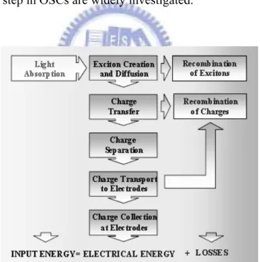
Figure 1.1 Progress of research-scale photovoltaic device efficiencies, under AM 1.5 simulated solar illumination for a variety of technologies (as compiled by Larry Kazmerski, National Renewable Energy Laboratory).…………...…….2 Figure 1.2 Schematic flow chart showing the important processes in organic solar cells.
Recombination of excitons can be radiative or non-radiative.………..…...……3
Chapter 2 Literature Review
Figure 2.1 Schematic diagram of roll-to-roll process of OSC modules (from Konarka Technologies, Inc.).………...…….10 Figure 2.2 Development of flexible printed circuit boards.………...……..….12 Figure 2.3 Schematic diagram of the mechanism for direct metallization of a polyimide film
surface using an ion-doped precursor layer. (A) Reduction of copper ions via self-oxidative decomposition of DMAB in aqueous solution. (B) Formation of copper atoms followed by protonation of the remaining carboxylate anion groups. (C) Ion-exchange reaction between protons and copper ions through the generation of a concentration gradient of these ions in the precursor layer, and further reduction of copper ions at the film surface.………...14 Figure 2.4 Effect of DMAB reduction temperature on the peel strength of the resulting
copper film formed on the surface-modified polyimide film.……….14 Figure 2.5 Transparency of a 30-nm-thick nanotube film with 200 Ω/sq. sheet resistance,
together with the transparency of ITO on glass 15 Ω/sq.………...….17 Figure 2.6 Metal-insulator-metal (MIM) picture of organic diode device function. (a) Closed circuit condition: under illumination photogenerated charges drift toward the contacts. (b) Flat band or open circuit condition: the current becomes zero. (c) Reversed bias: photogenerated charges drift in strong electric fields, the diode operates as a photodetector. (d) Forward bias larger than VOC: the injection increases and the diode opens up………...….20 Figure 2.7 Schematic representation of general excitonic mechanism for photoenergy
conversion in organic solar cells.…………...….22 Figure 2.8 Schematic representation of elementary steps in the process of photoinduced
donor; (2) diffusion of the exciton and formation of an encounter pair; (3) electron transfer within the encounter pair to form a geminate pair; (4) charge separation………....23 Figure 2.9 Schematic diagrams of built-in potential in metal/polymer/metal structures…....25 Figure 2.10 Open-circuit voltage (Voc) of different bulk-heterojunction solar cells plotted
versus the oxidation potential/HOMO position of the donor polymer used in each individual device...….25 Figure 2.11 Current-voltage curve of (P3HT)/PCBM solar cell measured in the dark (solid line) and field-driven photocurrent (dotted line). The built-in potential VBI is given by ELUMO(PCBM) minus EHOMO(P3HT) (-4.3 V- (-5.1 V) = 0.8 V)..25 Figure 2.12 Schematic diagrams of different types of excitons in organic semiconductors...27 Figure 2.13 Several solution processible conjugated polymers and a fullerene derivative used in organic solar cells. Upper row: the p-type holeconducting donor polymers MDMO-PPV, P3HT and PFB. Lower row: the electronconducting acceptor polymers CN-MEH-PPV and F8BT and a soluble derivative of C60, PCBM (1-(3-methoxycarbonyl) propyl-1-phenyl[6,6]C61)………...28 Figure 2.14 Several small molecular materials used in organic solar cells. Donor (p-type)
materials: ZnPc, CuPc, Me-PTCDI, Pentacene and PTCDA. Acceptor (n-type) materials: C60, NTCDA and DAAQ. Exciton blocking material: BCP.……….29 Figure 2.15 The most common device architectures for organic solar cells. Material B is any organic material. A is an electron acceptor material and D is an electron donor material.………..….32 Figure 2.16 Illustration of the difference between a real and an ideal I-V curve. The area of the inner rectangle corresponds to the maximal output power of the real device (at the maximum power point), whereas the area of the outer rectangle formed by the axes and the ideal I-V curve is equivalent to the maximum ideal output power.………...………..….34 Figure 2.17 Equivalent circuit diagrams for a solar cell.………...……...….……..….35 Figure 2.18 Number of photons (Nph) absorbed in the active layer under AM 1.5G calculated
by transfer-matrix formalism (TMF), for a device having the following structure: glass (1 mm)/ITO (140 nm)/PEDOT:PSS (50 nm)/P3HT:PCBM (x nm)/Al (100 nm). The right axis represents the corresponding short-circuit current density Jsc at various IQE, indicated in the graph...……...……..….38
Figure 2.19 The two most commonly used standard spectra, AM 1.5 direct and AM 1.5 global. The global spectrum comprises the direct plus the diffuse sunlight. The difference is mainly in the shorter wavelength region since molecular scattering scales with λ4. Water (H2O), ozone (O3) and carbondioxide (CO2) are the main
absorbers of the solar radiation in Earth’s atmosphere.……...………..….39 Figure 2.20 Schematic representation of the different AM sun light spectra.……….40 Figure 2.21 Schematic representation of the different AM sun light spectra.……….41
Chapter 3 Materials and Experimental Techniques
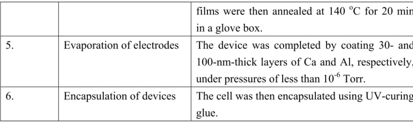
Figure 3.1 Photographs of polymer/fullerene solar cells with (A) P/ITO anode, (B) surface-modified PEDOT:PSS anode...….52 Figure 3.2 (A)-(E) Flow chart for the fabrication of the inverted PSCs on NiPI films. (F) The
photograph of the inverted PSCs on NiPI films...….54
Chapter 4 Chemical Formation of Palladium-free Surface-nickelized Polyimide Film for Flexible Electronics
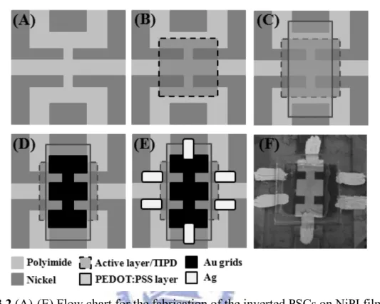
Figure 4.1 Flow chart of formation of surface-nickelized polyimide films: (a) PI film: Pristine polyimide (b) K+/ PI film: K+/ PAA layer on PI film, (c) Ni2+/ PI film: Ni2+/ PAA layer on PI film, (d) Ni-NPs/ PI film: Ni-NPs/ PAA layer on PI film, (e) Ni / PI films: Ni/ PAA layer on PI film...….62 Figure 4.2 ATR-FTIR absorption spectra of polyimide modified with KOH for different
time………..………65 Figure 4.3 ATR-FTIR absorption spectra of (a) pristine PI film, (b) K+/ PI films, (c) Ni2+/ PI film, (d) Ni-NPs/ PI film, (e) Ni-NPs/ PI film-310: Ni-NPs/ PI film after annealing at 310 oC for 1hr, and (f) Ni/ PI film.……….………67 Figure 4.4 XRD patterns of (a) pristine PI film, (b) Ni-NPs/ PI film-110 (annealed at 110 oC for 1 hr), (c) Ni/ PI film-110 (annealed at 110 oC for 1 hr), and (d) Ni/ PI film-310 (annealed at 310 oC for 1hr)...……….………...………69 Figure 4.5 Variation of contact angle of PI surface in the alkaline hydrolysis after treatment
with KOH and then ion exchange with nickel ions.….………...………70 Figure 4.6 Dependence of transparency and appearance of Ni-NPs/ PI films (Ni-NPs/ PI film treated with KOH(aq.) for X min/ NiSO4(aq.) for 5 min/ NaBH4(aq.) for 30 min at 50
oC) on hydrolysis time (X min) during KOH treatment: (A) 0 min, (B) 5 min, (C) 10 min, (D) 20 min, (E) 30 min, (F) 60 min, (G) 120 min.………...…………..73
Figure 4.7 AFM photographs of nanostructured Ni-NPs/ PI films (Ni-NPs/ PI film treated with KOH(aq) for 10 min/ NiSO4(aq.) for 5 min/ NaBH4(aq.) for 30 min at 50 oC)
for various hydrolysis times with KOH treatment: (A) 0 min, (B) 5 min, (C) 30 min, (D) 60 min. (left: top-view diagram; range of z is 200 nm; right: phase diagram, range of z is 200 degree).………...…..75 Figure 4.8 FE-SEM images of electroless-plated nickel on Ni-NPs/ PI films (Ni-NPs/ PI film treated with KOH(aq) for 30 min/ NiSO4(aq) for 5 min/ NaBH4(aq) for 30 min at 50 oC) at 50 oC for (A) 0 min, (B) 2 min, (C) 4 min, (D) 6 min, (E) 10 min, (F) 15 min. White bars represent 200 nm. (left: top-view, right: tilt 45o-view). XPS spectra of Ni-NPs/ PI films. (a) Ni-NPs/ PI film-d (measured directly), (b) Ni-NPs/ PI film-a (measured after one day).……….…...…..77 Figure 4.9 TEM photographs of cross section of Ni-NPs/ PI film (Ni-NPs/ PI film treated
with KOH(aq) for 10 min/ NiSO4(aq.) for 5 min/ NaBH4(aq) for 30 min at 50 oC).
The bar represents 100 nm. The A-area and B-area are outside and inside the Ni-NPs layer, respectively.………...…...……...79 Figure 4.10 TEM photographs (left) and EDX analysis (right) of cross section of
surface-nickelized PI films: A-the Ni layer, B-the Ni-NPs layer, C-PI film...79 Figure 4.11 Variations of contact angle of two PI sides in the alkaline hydrolysis after
treatment with KOH...82 Figure 4.12 TEM photographs of cross section of Ni-NPs/ PI film (Ni-NPs/ PI film treated
with KOH(aq) for 10 min/ NiSO4(aq) for 5 min/ NaBH4(aq) for 5 min/ EN solution for 10 min at 50 oC). (A) A side of PI film. (B) B side of PI film...83 Figure 4.13 Peel strengths of two sides of Cu/Ni/PI films and Cu with various thicknesses.84
Chapter 5 High-Conductivity Poly(3,4-ethylenedioxythiophene):Poly(styrene sulfonate) Film for Use in ITO-Free Polymer Solar Cells
Figure 5.1 Architecture and photograph of the ITO-free polymer/fullerene solar cell...89 Figure 5.2 Raman spectra of PEDOT:PSS films excited using HeNe laser at 632.8 nm...93 Figure 5.3 SEM cross-sectional images of solvent-modified PEDOT-PSS films on glass
substrates. (a) P, (b) P-ET, (c) P-ME, (d) P-DME and (e) P-EG...94 Figure 5.4 Topographic (A, C, E) and phase (B, D, F) images of PEDOT-PSS films (P, P-ME
and P-EG, respectively) obtained with tapping-mode AFM...96 Figure 5.5 TEM images of solvent-modified PEDOT-PSS films. (A) P, (B) P-ET, (C) P-ME,
Figure 5.6 C(1s) core level spectra before and after heat treatment of (a) P-na, (b) P, (c) P-ET, (d) P-ME, (e) P-DME, and (f) P-EG...100 Figure 5.7 O(1s) core level spectra before and after heat treatment of (a) P-na, (b) P, (c) P-ET,
(d) P-ME, (e) P-DME, and (f) P-EG...101 Figure 5.8 S(2p) core level spectra before and after heat treatment of (a) P-na, (b) P, (c) P-ET,
(d) P-ME, (e) P-DME, and (f) P-EG...101 Figure 5.9 Schematic 3D morphological models of (A) P (top-view), (B) P (side-view), (C)
P-ME (top-view), (D) P-ME (side-view), (E) P-EG (topview), (F) P-EG (side-view)……….104 Figure 5.10 Current–voltage characteristics of ITO-free polymer solar cells incorporating the various solvent-modified PEDOT:PSS films: (a) P, (b) P-ET, (c) P-ME, (d) P-DME, and (e) P-EG. All devices were measured under illumination of AM 1.5 (100 mW cm-2) with active area of 0.01 cm2...107
Chapter 6 All-Solution-Processed Inverted Polymer Solar Cells on Granular Surface-Nickelized Polyimide
Figure 6.1 Architectures of polymer solar cells: (A) standard, (B) inverted (in terms of the roles of the electrodes), and (C) inverted (in terms of the alternative processing structure)...113 Figure 6.2 Flow chart for the formation of the patterned NiPI film. (A) PI: pristine polyimide;
(B) K+/PI: K+/PAA layer on PI film; (C) Ni2+/PI: Ni2+/PAA layer on PI film; (D)
Ni-NPs/PI: Ni-NPs/PAA layer on PI film; (E) NiPI: Ni/PAA layer on PI film; (F) Patterned NiPI: patterned Ni/PAA layer on PI film; (G) photograph of the patterned NiPI. (a) Alkaline hydrolysis to open imide rings; (b) cation-exchange reaction leading to the incorporation of Ni2+ ions; (c) reduction of Ni2+ ions by aqueous NaBH4; (d) Ni electroless plating using an EN solution; (e) patterning
of Ni through photolithography...114 Figure 6.3 (A) Photoelectron spectrum of NiPI film. (B) XPS spectrum of NiPI surface. (C) SEM image of NiPI surface. (D) Schematic representation of the energy levels of an ITO-free inverted PSC on PI...120 Figure 6.4 (A) S(2p) core level spectra of P3HT:PCBM film (1:0.8 w/w) with plasma
treatment for various seconds. (B) Architecture of an inverted PSC featuring an inverted sequence on NiPI as the back contact electrode. (C) Optical image of an inverted PSC on NiPI. (D) TEM cross-sectional image of an inverted PSC on
NiPI. Scale bars, 500 nm...123 Figure 6.5 (a, c, e, g) Topographies (including cartoon representations) and (b, d, f, h) phase images of NiPI and TIPD-modified NiPI films. (a, b) NiPI: pristine NiPI film; (c, d) T0NiPI: TIPD (0.94 wt%) on NiPI film; (e, f) T3NiPI: TIPD (3.75 wt%) on NiPI film; (g, h) T15NiPI: TIPD (15 wt%) on NiPI film. Scale bars, 500 nm.129 Figure 6.6 I–V characteristics of inverted PSCs under AM 1.5 illumination (100 mW
cm–2) ……….130
Figure 6.7 SEM images (Top-view) of different structure of cathodes. (A) AlPI: planar AlPI, (B) NiPI: granular NiPI. (C) Reflective UV-vis spectra of films on different structures of cathodes. (a) AlPI: planar AlPI, (b) NiPI: granular NiPI, (c) PT3/AlPI: P3HT:PCBM/TIPD(3.75 wt%)/AlPI, (d) PT3/NiPI: P3HT:PCBM/TIPD (3.75 wt%)/NiPI, (e) PT3AlPI Device: PEDOT:PSS/PT3/ AlPI, (f) PT3NiPI Device: PEDOT:PSS/PT3/NiPI.………..133 Figure 6.8 (A) Reflection haze factors for different structure of cathodes and the EQE
spectra of inverted PSCs on different structure of cathodes. Cartoon representations for inverted PSCs illuminated on different structure of cathodes. (B) Planar AlPI, (C) Granular NiPI.……….……….134
Chapter 7 Morphological Control of CuPc and its Application in Organic Solar Cells
Figure 7.1 Organic donor–acceptor heterojunctions: (a) planar, (b) mixed DA, (c) thermodynamically driven bulk, and (d) ideal bulk heterojunctions.……..….139 Figure 7.2 SEM images of TE-grown CuPc films on (a) ITO, (b) PITO, (c) AITO (top-view),
and (d) AITO (side-view) substrates. The cartoon images (a)-1~(c)-1 represent the morphologies in (a)~(c), respectively..………....142 Figure 7.3 SEM images of vertical rod-like CuPc films grown on Au substrates at
thicknesses (measured using a quartz crystal microbalance) of (a) 100, (b) 200, (c) 300, and (d) 500 Å. (e) Cartoon representation of an ideal BHJ of CuPc films. All scale bars are 100 nm...………...144 Figure 7.4 GIXRD spectra of CuPc powders and films deposited on various substrates at
various substrate temperatures: (a) AITO (Tsub = 25 °C), (b) AITO (Tsub = 100
°C), (c) PITO (Tsub = 100 °C), (d) ITO (Tsub = 100 °C), and (e) CuPc
powders……….145 Figure 7.5 (a) SEM (top-view) image of a thin layer of Au on an ITO substrate. (b)–(d) TEM
Tsub = 100 °C. (b) Bottom section of CuPc rods. (c) CuPc rods. (d) HR-TEM images of the upper section of CuPc rods.………...……….147 Figure 7.6 AFM images [topographic (a) and phase (b)] of the PITO surface. SEM images
[top-view (c) and estimate (d)] of CuPc rod-like film on the PITO. (e) S(2p) core level spectra of the PITO surface...……….150 Figure 7.7 (A) Schematic representation of the energy levels of the devices. (B) UV–Vis
spectral transmittance of fully processed solar cells incorporating various films: (a) ITO, (b) AITO, (c) rod-like CuPc (200 Å)/AITO, (d) C60 (300 Å)/CuPc:C60 (1:1) (100 Å)/ rod-like CuPc (200 Å)/AITO. (C) Cross-sectional image of the device having the structure AITO/CuPc (200 Å)/CuPc:C60 (100 Å)/C60 (300 Å)/BCP (75 Å)/Al.………...…….153 Figure 7.8 (A) Cartoon representations of four types of DA interfaces in solar cells. (B) J–V
curves of devices possessing the configuration anode/CuPc (200 Å)/CuPc:C60 (1:1) (100 Å)/C60 (300 Å)/ BCP (75 Å)/Al under illumination (100 mW cm-2), featuring various CuPc morphologies formed under various annealing temperatures.……...…….156
Chapter 8 Conclusions and Prospects
Chapter 1 Introduction
Chapter 1
Introduction
1.1 Background
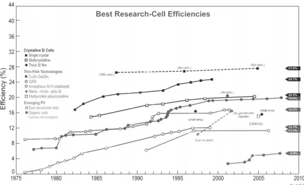
Supply of energy is one of the main concerns of our society. Because of growing economy and modern lifestyle, consumption of energy rises drastically. The world’s fossil energy resources are still ample for the next coming years –yet, the extraction costs for this kind of energy is still under debate. The current oil prize instability reveals the vulnerability of our economy towards higher energy prizes, not mentioning the political and economical unrest predominant in several main oil producing countries. Because our world highly depends on those supplies, there is a risk of slipping into an energy crisis someday soon. Therefore, over the past several decades, there are a lot of countries to invest large amount of capitals and time in developing the renewable sources of energy. Among the developments of power producing, the direct conversion of solar energy to electricity by photovoltaic (PV) is emerging as a leading contender for next-generation green power production. Conversion into electrical power of even a small fraction of the solar radiation incident on the Earth’s surface has the potential to satisfy the world’s energy demands without generating CO2 emissions. The progress in the efficiency of
Chapter 1 Introduction
Figure 1.1 Progress of research-scale photovoltaic device efficiencies, under AM1.5
simulated solar illumination for a variety of technologies (as compiled by Larry Kazmerski, National Renewable Energy Laboratory).
Current PV technology is not yet fulfilling this promise, largely due to the high cost of the electricity produced. Although the challenges of storage and distribution should not be underestimated, a major bottleneck lies in the PV devices themselves. Improving efficiency is part of the solution, but diminishing returns in that area mean that reducing the manufacturing cost is absolutely vital, while still retaining good efficiencies and device lifetimes. Although the PV technology platforms of silicon-based PV and thin-film PV are now undergoing a rapid expansion in production and the power conversion efficiency can easily approach 15% [1], their high costs of fabrication and of raw materials have yielded limited commercial applications. Recently, the next generation PV—organic solar cells
(OSCs)—could soon be playing a major role with the advantages of low-cost, large-area, lightweight and shatterproof. The challenge here is that absorbing light in an organic material produces a coulombic bound exciton that requires dissociation at a
Chapter 1 Introduction
incident light, but excitons only diffuse a few nanometres before decaying. The problem is therefore intrinsically at the nano-scale: the composite devices with a large area of internal donor–acceptor interface are needed, but where each carrier has a pathway to the respective electrode. Following this is the separation of charges which is mostly induced by the field generated from the difference in work functions of the electrodes. The following scheme shows the important processes in OSCs (Figure 1.2). At each one of these steps, recombination of the electron and hole can occur, preventing their contribution to the current. In addition to the fundamental restrictions of the device, such as how much light can be absorbed, these recombination losses limit the overall maximum efficiency of energy conversion that can be attained. So that the issues on how to overcome the problems form each step in OSCs are widely investigated.
Figure 1.2 Schematic flow chart showing the important processes in organic solar cells.
Recombination of excitons can be radiative or non-radiative.
Flexible electronics are increasingly being used in a number of applications which benefit from their low production cost, light weight, favorable optical and electrical properties. However, despite these advantages, the range of practical, high-volume,
Chapter 1 Introduction
applications for flexible electronics will remain limited in the future unless a number of challenges related to electrical performance and stability on flexible substrates are compared to the standard devices. Although researchers generally investigate the OSCs on rigid ITO/glass substrates, the final developing objective of OSCs is fabricated on flexible substrates to exhibit the advantages of OSCs. In the developing field of production technologies of flexible electronics, the highest productivity at lowest process costs is gained from roll-to-roll processing. The manufacture of the flexible electronics can be integrated several printing techniques (such as inkjet, screen, flexographic and gravure printings) into the roll-to-roll process to enhance the throughput of products [2-5]. Based on the previous considerations, in this thesis, I will develop several techniques of solution processes to produce the roll-to-roll suitable circuits and electrodes and apply those methods in the flexible OSCs.
Chapter 1 Introduction
1.2 Aims and Objectives
It will be demonstrated in this thesis that several investigations of key technologies of circuits and electrodes for applying in flexible electronics, especially in OSCs. In the present work, I will develop an all-solution method for fabricating thin Ni films on PI (NiPI) with high adhesion and conductivity and it will be suitable for roll-to-roll manufacturing processes in flexible printed circuits. Furthermore, I will devise a simple method to enhance the conductivity of PEDOT:PSS films through spin-coating with various surface-modified compounds, and then apply the PEDOT:PSS films as anodes to the preparation of ITO-free polymer solar cells (PSCs). The ultimate goal is to prepare all-solution-processed inverted polymer solar cells (PSCs) incorporating two solution-processed electrodes—NiPI films as cathodes and high-conductivity PEDOT:PSS films as anodes—on flexible substrates.
Another developing field of electrodes will be studied to control the morphology of active layers in the small molecular solar cells, and therefore I will investigate the rod-like CuPc structures on indium–tin oxide (ITO), PEDOT:PSS and Au substrates to demonstrate an ideal bulk heterojunction structure using the self-assembly of CuPc as the donor material and fullerene as the acceptor.
The objectives of this thesis are as follows:
To study and review relevant literatures on surface-metalized PI films.
To develop a simpler way to fabricate a metal thin film (as the conducting and diffusion barrier layer) on PI films, and excellent adhesion between the metal and PI phases will be obtained.
To study and review relevant literatures on the solution-processed transparent conducting layers.
Chapter 1 Introduction
To investigate the origin effect of conductivity enhancement of PEDOT:PSS films from the comprehensive analysis results.
To demonstrate the ITO-free PSCs with the high-conductivity PEDOT:PSS films and understand the limits for larger area cells.
To study and review relevant literatures on inverted PSCs and the solution-processed techniques of PSCs.
To investigate the interface problems of fabricating inverted PSCs on NiPI films. To inspect the optical properties occurring in NiPI-based PSCs and recommend how
to improve the performance in the next generation of PSCs.
To study and review relevant literatures on small molecular solar cells.
To investigate the morphological control of CuPc and its application in organic solar cells.
To calculated the surface energy difference of PEDOT and PSS phases, and recommend how to improve the performance in the next generation of small molecular solar cells.
Chapter 1 Introduction
1.3 Brief Structures of this Thesis
This thesis comprises eight chapters. Contents of each chapter are detailed as follows:
Chapter 1 provides the background of this study, stating the reason why the study is conducted. In addition, the aims and objectives of this thesis are outlined in this chapter.
Chapter 2 is literature review of research in the field of circuits, electrodes and organic solar cells. Key area focuses on the fabrication of all-solution-processed electrodes for application of flexible printed circuits and organic solar cells (such as polymer solar cells and small molecular solar cells).
Chapter 3 is a short overview of the materials used and the experimental details that we developed for reproducible device preparation will be presented.
Chapter 4 represents the theory and formation of surface-nickelized polyimide films using a wet chemical process. This investigation will synthesize nickel nanoparticles as seeds (catalysts) and a Ni metal layer as an adhesion-promoting layer on the surface of a polyimide film, and excellent adhesion between the nickel and polyimide phases was observed. It can reduce the cost of the catalyst and simplify the process of coating the adhesion-promoting layer on the PI film.
Chapter 5 describes the goal and experiment methodology to develop a simple method for modifying the electrical conductivity of PEDOT:PSS films intended for use as electrodes in ITO-free solar cells. The high-conductivity PEDOT:PSS films could be obtained simply through spin-coating of a solvent onto pre-coated PEDOT:PSS films. We employed the comprehensive analysis results to determine the origin of the conductivity enhancement.
Chapter 1 Introduction
We found that the performance of the PPVs was related to the surface morphologies, chemical structures, and electrical conductivities of the PEDOT:PSS films. We performed a comprehensive investigation of the effects of alcoholic and ethereal solvents, including methoxyethanol, ethanol, and 1,2-dimethoxyethane, to determine the driving force for the conductivity enhancement of the PEDOT:PSS films.
Chapter 6 reports the fabrication of all-solution-processed inverted PSCs featuring granular NiPI as the cathode material (back contact electrode) on flexible substrates; combining with the techniques in chapter 4 and chapter 5, these devices have the following configuration: PI/Ni (cathode)/ titanium(diisopropoxide)bis (2,4-pentanedionate (TIPD)/P3HT:PCBM/PEDOT:PSS (anode). Furthermore, when compared to the planar structure, the improvement of absorbance of light and good haze factors was obtained for granular structure which suggests NiPI as a better back contact electrode through enhancing the light trapping and scattering in inverted PSCs.
Chapter 7 reports the organic photovoltaic (OPV) cells possessing an ideal bulk heterojunction (BHJ) structure using the self-assembly of copper phthalocyanine (CuPc) as the donor material and fullerene (C60) as the acceptor. The variable self-assembly behavior
of CuPc on a diverse range of substrates (surface energies) allowed us to control the morphology of the interface and the degree of carrier transportation within the active layer.
Chapter 8 draws conclusions from the results and discussions. In addition, some prospects are made for future research.
Chapter 2 Literature Review
Chapter 2
Literature Review
2.1 Polymer Substrates
Polymer has attracted a great deal of concern in the past few years because polymers can be applied to the manufacturing of various electronic and display devices. There have been extensive research activities on flexible electronics based on polymer materials. Flexible printed circuit board (FPCB), packaging, and flexible organic solar cells (OSCs) based on all polymeric materials or partial employment of polymeric materials have been developed due to low cost and ease of fabrication. It is expected that micro-electro-mechanical systems (MEMS) and semiconductor devices as well as flexible displays can be fabricated on flexible substrate for many applications. It is because that flexible electronics offer substantial coupled rewards in terms of being able to develop electronics that are thinner, lighter, robust and can be rolled away when not required. In addition, plastic-based substrates coupled with the recent developments in solution deposition and inkjet printing for laying down electronic materials open up the possibility of cost-effective processing in high volumes using roll-to-roll processing. For instance, polymer solar cells can be created using roll-to-roll manufacturing process. The roll-to-roll process is the process in which transparent electrode, printed active material, primary electrode and substrate are printed onto transparent packaging to make a solar panel. This manufacturing process is inexpensive, environmental friendly, and simple. The schematic diagram of roll-to-roll process of OSC modules is shown in Figure 2.1.
Chapter 2 Literature Review
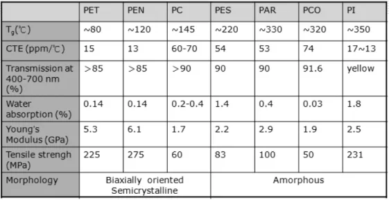
and a variety of plastics. Therefore, to replace glass, a plastic substrate needs to be able to offer the properties of glass, i.e. clarity, dimensional stability, thermal stability, barrier, solvent resistance, low coefficient of thermal expansion (CTE) coupled with a smooth surface. This section will focus only on plastic films that have been given serious consideration as flexible substrates for flexible electronics. Based on different process temperatures and product demands, the suitable polymer substrate can be selected in further applications. The main candidates are shown in Table 2.1 [6].
Figure 2.1 Schematic diagram of roll-to-roll process of OSC modules (from Konarka
Technologies, Inc.).
Table 2.1 Basic properties of polymers used for base substrate. (Note: PET: Polyethylene
terephthalate; PEN: Polyethylene naphthalate; PC: Polycarbonate; PES: Polyethersulphone; PAR: Polyarylate; PCO: Polycyclic olefin; PI: Polyimide.)
Chapter 2 Literature Review
2.2 Flexible Printed Circuit Boards
Recently, polyimide (PI) films have become generally used components for flexible electronic devices because they exhibit high glass transition temperatures, low surface roughness, low coefficients of thermal expansion (CTE), and high chemical resistance under typical fabrication conditions. Therefore, metallization of polyimide for metal lines has therefore been the subject of intense study for FPCB, [7-11] with various trials having been conducted in incorporating metal wiring layers onto dielectric polyimide, with the aim of developing high performance microchips. The base materials of FPCB and other soft electronics are copper on polyimide with or without adhesive. The former is called the three-layer mode (3L-FPCB: metal/adhesive/PI), while the latter is the two-layer mode (2L-FPCB: metal/PI). The development of FPCB with smaller line widths and increased wire density is based on the two-layer (Figure 2.2). For example, one common approach is photolithography utilizing a photoresist combined with metal coating on a polyimide substrate in an additive (area-selective deposition of metals by physical and chemical means) and/or subtractive (etching of preformed metal films) manner [7-11]. Another approach is electroless deposition combined with simultaneous or alternating laser irradiation [12, 13]. However, this process sometimes has undesired defects in the pattern due to laser-induced decomposition of the polyimide substrate. The development of a facile, direct metallization process with which metallic patterns could be directly formed onto polyimide substrates is challenging. In addition, device fabrication processes require high reliability in terms of the adhesive strength between the thin metal films and the underlying substrate. To achieve sufficient adhesion between the metal film and polyimide, most conventional metallization processes employ etching of the polyimide surface (typically several micrometers in surface roughness), leading to an increase in contact area to provide good adhesion through mechanical interlocking (anchoring). [7-11] However,
Chapter 2 Literature Review
as the dimensions of pattern details drop to the several micrometer and submicrometer scales, micrometer scale anchoring is not suitable for reliable adhesion. Thus, a new adhesion method is required for realizing future generations of electronic devices.
Figure 2.2 Development of flexible printed circuit boards.
Recently, Kensuke and Hidemi et al. reported a novel surface-modification based method for the metallization of polyimide surfaces. [14-18] The method relies on a simple alkali treatment of the bare polyimide films to introduce the active components of an ion exchange reaction (carboxylic acid groups) [19, 20] and subsequent loading of metal ions into the modified layers by ion exchange reactions. Fabrication of the metallic thin films or patterns was previously achieved through chemical reduction using NaBH4 aqueous
solution [14] and ultraviolet (UV)-light-induced photochemical reduction of the adsorbed metal ions using preadsorbed TiO2 nanocrystals as a photocatalyst on the polyimide
surface. [16] Although this process allows the polyimide surface to be metallized directly, the formation of metallic thin films is only achieved through the use of a photoresist or
Chapter 2 Literature Review
polyimide is difficult to control. It is suggested that the diffusion of metal ions during the reduction process plays a key role in determining the metal/polyimide interfacial structures. The following schematic diagram showed that mechanism for direct metallization of a polyimide film surface using an ion-doped precursor layer (Figure 2.3). [18] Furthermore, when using this surface metalized Cu/PI films to apply in FPCB, the copper film side and the polyimide substrate side of the samples obtained can achieve an average adhesive strength of 1.00 kg fcm–1 (Figure 2.4).
Chapter 2 Literature Review
Figure 2.3 Schematic diagram of the mechanism for direct metallization of a polyimide
film surface using an ion-doped precursor layer. (A) Reduction of copper ions via self-oxidative decomposition of DMAB in aqueous solution. (B) Formation of copper atoms followed by protonation of the remaining carboxylate anion groups. (C) Ion-exchange reaction between protons and copper ions through the generation of a concentration gradient of these ions in the precursor layer, and further reduction of copper ions at the film surface.
Chapter 2 Literature Review
2.3 Electrode Materials
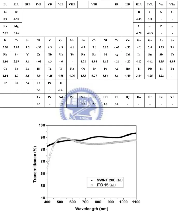
In the electronics, the work function (WF) of the electrode materials is very important since it determines together with the LUMO/HOMO and Fermi-level of the semiconductor whether the electrode forms an ohmic or a blocking contact for the respective charge carrier (holes in valance band, electrons in conducting band). In Table 2.2, the periodic table of the elements is listed with its values of WF [21]. The values in Table 2.2 are valid only for poly-crystalline materials. However, many numbers for single crystals which depend on its crystallographic orientation have also been reported [21]. The general electrode materials can be categorized as metal, inorganic semiconductor, conducting polymer and carbon nanotube (CNT) materials. Common metal electrode materials for the electron collecting contact (low WF required) of organic solar cells are Al, Ca, Ag whereas for the hole collecting contact high WF materials like Au are preferred. If the metal materials are used to apply in flexible printed circuits (FPC), the conductivity and adhesion properties of circuits are the major issues. The metals for FPC are usually selected Cu, Ag, Au (high conductivity) as the electron conduction layers and Ni, Cr, Ti as the adhesion-promoting layers [22, 23]. While indium tin oxide (ITO) materials are usually used as transparent conducting layer, which is a degenerated semiconductor comprising a mixture of In2O3 (90%) and SnO2 (10%) with a band gap of 3.7eV and a
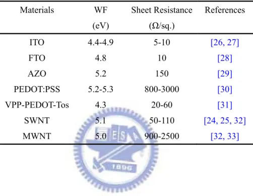
Fermi-level between 4.5 and 4.9eV is widely used. The large band gap allows no absorption of wavelengths longer than about 350nm. Unfortunately, the high cost of high-quality ITO and its lack of flexibility can limit the applications of electronics incorporating it as an anode material; the limited supply of indium and the transparency of ITO toward visible light are additional problems. Recently the ITO-free conducting materials, such as PEDOT:PSS and CNT films, are widely investigated to replace ITO in the future. An additional advantage of PEDOT:PSS is that it can be manufactured through
Chapter 2 Literature Review
the solution processes. CNT network films appear to be a suitable alternative: they can be prepared through solution processing, and they exhibited high conductivity and flexibility
[24, 25]. Figure 2.5 shows the transparency and conductivity of single-walled carbon nanotube network films [24]. Furthermore, the stability of devices fabricated on the SWNT/PET films is much greater than devices on ITO/PET during simple bending tests. The PSCs with SWNT network films as electrode could be folded over (inducing compressive or tensile strain) down to radii of curvature of ~5 mm with no degradation in power efficiency and radii of ~1 mm with a 20-25 % loss in efficiency. Such CNT-based devices do, however, have their problems. For example, the nature of the transparent single-wall carbon nanotube (SWNT) network films is not always well defined; typically, SWNT films are mixtures of metallic and p-doped nanotubes. In addition, it is necessary to add PEDOT:PSS to adjust the work function of the SWNTs and to avoid shorting of the device. Therefore, recently the PEDOT:PSS materials are widely investigated to enhance the conductivity and then used to apply in ITO-free devices. Some transparent conducting materials are listed with their WF, sheet resistance and references in Table 2.3.
Chapter 2 Literature Review
Table 2.2 WF of the elements. The numbers refer to the WF (eV) of the elements in
polycrystalline form.
IA IIA IIIB IVB VB VIB VIIB VIII IB IIB IIIA IVA VA VIA Li 2.9 Be 4.98 B 4.45 C 5.0 N - O - Na 2.75 Mg 3.66 Al 4.28 Si 4.85 P - S - K 2.30 Ca 2.87 Sc 3.5 Ti 4.33 V 4.3 Cr 4.5 Mn 4.1 Fe 4.5 Co 5.0 Ni 5.15 Cu 4.65 Zn 4.33 Ga 4.2 Ge 5.0 As 3.75 Se 5.9 Rb 2.16 Sr 2.59 Y 3.1 Zr 4.05 Nb 4.3 Mo 4.6 Tc - Ru 4.71 Rh 4.98 Pd 5.12 Ag 4.26 Cd 4.22 In 4.12 Sn 4.42 Sb 4.55 Te 4.95 Cs 2.14 Ba 2.7 La 3.5 Hf 3.9 Ta 4.25 W 4.55 Re 4.96 Os 4.83 Ir 5.27 Pt 5.56 Au 5.1 Hg 4.49 Ti 3.84 Pb 4.25 Bi 4.22 Po - Fr - Ra - Ac - Th 3.4 Pa - U 3.63 Ce 2.9 Pr - Nd 3.2 Pm - Sm 2.7 Eu 2.5 Gd 3.2 Tb 3.0 Dy - Ho - Er - Tm - Yb -
Figure 2.5 Transparency of a 30-nm-thick nanotube film with 200 Ω/sq. sheet resistance, together with the transparency of ITO on glass 15 Ω/sq.
Chapter 2 Literature Review
Table 2.3 WF and sheet resistance of the transparent conducting electrode materials. (Note:
Indium tin oxide (ITO); Fluorine-doped tin oxide (FTO); Aluminum-doped zinc oxide (AZO); poly(3,4-ethylenedioxythiophene)-poly(styrene-sulfonate) (PEDOT:PSS); vapor-phase polymerization poly(3,4-ethylenedioxythiophene)- Fe(III)-tosylate (VPP-PEDOT-Tos); Single-walled carbon nanotube (SWNT); Multi-walled carbon nanotube (MWNT).) Materials WF (eV) Sheet Resistance (Ω/sq.) References ITO 4.4-4.9 5-10 [26, 27] FTO 4.8 10 [28] AZO 5.2 150 [29] PEDOT:PSS 5.2-5.3 800-3000 [30] VPP-PEDOT-Tos 4.3 20-60 [31] SWNT 5.1 50-110 [24, 25, 32] MWNT 5.0 900-2500 [32, 33]
Chapter 2 Literature Review
2.4 Organic Solar Cells
Organic solar cells (OSCs) represent a rapidly emerging device technology with the potential for low-cost non-vacuum-processed devices. The key is that these devices combine the small molecular [34-36], polymer [37-40], organic-inorganic hybrid solar cells [41], and dye-sensitized solar cells [42-44]. In each type of OSCs the efficiency is limited by the absorption coefficient as a function of wavelength, the probability of excition dissociation into mobile charge carriers, the transport of those charges to the anode and cathode, and the collection of the carriers at the interfaces of electrode and organic phases. Although the excitonic mechanism is different from the conventional PV mechanism, the theoretical efficiency is the same as for conventional semiconductor devices, with a cost structure similar to that for plastics processing, leading to the potential for significant reductions in cost per watt. In this thesis, I focus on the investigation of polymer and small molecular solar cells.
2.4.1 Principle of Operation
To understand the rectifying behavior of an intrinsic (nondoped) semiconductor device in the dark, the MIM (metal-insulator-metal) model is useful [45]. In Figure 2.6, a semiconductor, sandwiched between two metal electrodes with different work functions is depicted for several situations. The metals are represented by their Fermi levels, whereas for the semiconductor the valence and conduction bands, corresponding to the molecular LUMO (lowest unoccupied molecular orbital) and the HOMO (highest occupied molecular orbital) levels, are shown. In Figure 2.6(a), there is no voltage applied (i.e., short-circuit conditions). Hence, there is no net current flowing in the dark, and the built-in electric field resulting from the difference in the metals’ work functions is evenly distributed throughout the device. Under illumination, separated charge carriers can drift in
Chapter 2 Literature Review
this electric field to the respective contacts: the electrons move to the lower work function metal and the holes to the opposite. The device then works as a solar cell. In Figure 2.6(b), the situation is shown for open circuit conditions, also known as “flat band condition.” The applied voltage is called the open circuit voltage Voc, which corresponds in this case to the
difference in the metals’ work functions and balances the built-in field. As there is no net driving force for the charge carriers, the current is zero. In Figure 2.6(c) the situation is shown for an applied reverse bias and only a very small injected dark current j0 can flow. Under illumination, the generated charge carriers drift under strong electric fields to the respective electrodes and the diode works as a photodetector. If a forward bias larger than the open circuit voltage is applied [Figure 2.6(d)], the contacts can efficiently inject charges into the semiconductor. If these can recombine radiatively, the device works as a LED. The asymmetric diode behavior results basically from the different injection of the two metals into the HOMO and LUMO levels, respectively, which depends exponentially on the energy barrier between them.
Figure 2.6 Metal-insulator-metal (MIM) picture of organic diode device function. (a)
Closed circuit condition: under illumination photogenerated charges drift toward the contacts. (b) Flat band or open circuit condition: the current becomes zero. (c) Reversed bias: photogenerated charges drift in strong electric fields, the diode operates as a photodetector. (d) Forward bias larger than VOC: the injection increases and the diode
Chapter 2 Literature Review
Efforts to optimize the performance of polymer and small molecular solar cells should find their basis in the fundamental mechanism of operation. Figure 2.7 illustrates the mechanism by which light energy is converted into electrical energy in the devices. The energy conversion process has six fundamental steps in the commonly accepted mechanism [46]:
(1) Absorption of light: The fraction of absorbed photons is a function of the absorption spectrum, the absorption coefficient, the absorbing layer thickness, and of internal multiple reflections at, for example, metallic electrodes.
(2) Generation of excitons: To achieve a high efficiency of charge generation, the active material in the solar cells should absorb as large a part of the solar light as possible. Upon absorption of a photon, an exciton is created in the active layer.
(3) Diffusion of the excitons: Ideally, all photoexcited excitons should reach a dissociation site. Since such a site may be at the other end of the semiconductor, their diffusion length should be at least equal the required layer thickness (for sufficient absorption), otherwise they recombine and photons were wasted. Exciton diffusion ranges in polymers and pigments are typically around 10 nm. However, some pigments like perylenes are believed to have exciton diffusion lengths of several 100 nm.
(4) Dissociation of the excitons with generation of charge: Charge dissociation is known to occur at organic semiconductor/metal interfaces, impurities (e.g. oxygen) or between materials with sufficiently different electron affinities (EA) and ionisation potentials (IA). In the latter one material can than act as electron acceptor (A) while the other keeps the positive charge and is referred to as electron donor (D) - since it did actually donate the electron to A. If the difference in IA and EA is not sufficient, the exciton may just hop onto the material with the lower bandgap without splitting up its charges. Eventually it will recombine without contributing charges to the photocurrent.
Chapter 2 Literature Review
(5) Charge transport: The transport of charges is affected by recombination during the journey to the electrodes - particularly if the same material serves as transport medium for both electrons and holes. Also, interaction with atoms or other charges may slow down the travel speed and thereby limit the current.
(6) Charge collection: In order to enter an electrode material with a relatively low workfunction (e.g. Al, Ca) the charges often have to overcome the potential barrier of a thin oxide layer. In addition, the metal may have formed a blocking contact with the semiconductor so that they can not immediately reach the electrodes.
The elementary steps involved in the pathway from photoexcitation to the generation of free charges are shown in Figure 2.8. [47, 48] The processes can also occur in an analogous fashion in the case of an excited acceptor, and the details of these mechanistic steps have been described extensively in the literature. [48] The key point is that electron transfer is not as simple as depicted in Figure 2.7. The process must be energetically favorable to form the geminate pair in step 3 of Figure 2.8 and an energetic driving force must exist to separate this Coulombically bound electron-hole pair.
Figure 2.7 Schematic representation of general excitonic mechanism for photoenergy
Chapter 2 Literature Review
Figure 2.8 Schematic representation of elementary steps in the process of photoinduced
charge separation for a donor (D) and an acceptor (A): (1) Photoexcitation of the donor; (2) diffusion of the exciton and formation of an encounter pair; (3) electron transfer within the encounter pair to form a geminate pair; (4) charge separation.
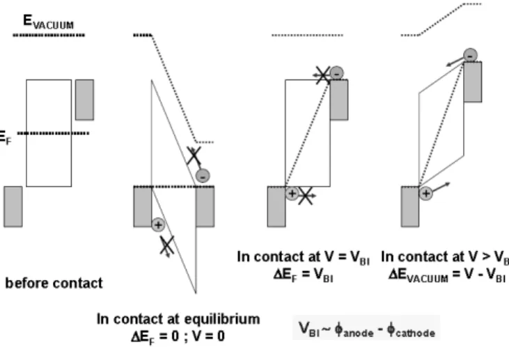
2.4.2 Built-in Potential
When applying the metal-insulator-metal (MIM) model to organic bulk heterojunction devices, the built in potential in organic semiconductor devices arises from the WF difference of the anode and cathode [49]. The schematic diagrams of built-in potential in metal/polymer/metal structures in Figure 2.9. However, even an extended MIM model was found to be insufficient for a complete explanation of the Voc of
bulk-heterojunction solar cells. Therefore, the effects of photocarrier distributions and chemical potential difference of energy level offsets at interfaces also require consideration in OSCs [50]. Based on the previous considerations, Markus et al. devised a simple relation between the energy level of the highest occupied molecular orbital (HOMO) of the polymer and the Voc is derived [51], which is used to estimate the
maximum efficiency of bulk-heterojunction solar cells. The results presented here can be used as a guideline for the selection and synthesis of new active materials for bulk-heterojunction solar cells. In Figure 2.10 the open-circuit voltage of different bulk-heterojunction solar cells is plotted versus the oxidation potential of the conjugated polymers used in these devices. Figure 2.10 demonstrates that for several bulk-heterojunction solar cells, a linear relation between Voc and the conjugated polymer
![Figure 2.14 shows several commonly used small molecular materials in OSCs [68-72]. Five important materials of hole-conducting donor type small molecular structures are listed as below: Zinc phthalocyanine (ZnPc); Copper phthalocyanine (CuPc), N,N’-dime](https://thumb-ap.123doks.com/thumbv2/9libinfo/8738028.203676/49.892.166.771.551.1059/molecular-materials-important-conducting-molecular-structures-phthalocyanine-phthalocyanine.webp)