Sloped-Gate Voltage Method for Improving Measurement of Poly-Si
Nanowire FET in Aqueous Environment
Chien-Hung Chen,
†,‡Yi-Jr Su,
§Chih-Heng Lin,
†Tai-Shan Liao,
‡Yuh-Shyong Yang,*
,†and Chi-Hung Hwang*
,‡†Institute of Biological Science and Technology, National Chiao Tung University, Hsinchu 300, Taiwan ‡Instrument Technology Research Center, National Applied Research Laboratories, Hsinchu 300, Taiwan §National Synchrotron Radiation Research Center, Hsinchu 300, Taiwan
*
S Supporting InformationABSTRACT: Nanowire field-effect transistors are suited to study the activity of biomolecules in bionanotechnology. The changes of biomolecules process are efficiently affected the charge at the nanowire surface; thus, the electrical character-ization of NW-FET is changed. Although NW-FET is a well-known device in bioapplications, however, the intrinsic electrical characterization of NW-FET effect on real electrical measurement is not well studied. We present herein a novel measurement method to avoid errors in electrical characteristic of nanowire field-effect transistors. A physical model is
developed to explore the effect of the leakage current, which is influenced by the charging effect of an equivalent capacitor in a NW-FET. We also present a sloped-gate voltage method to reduce the effect of equivalent capacitor in air, liquid, and phosphate buffered solution. The application of the sloped-gate voltage method significantly increases the stability of electrical characterization measurements. This method can also be easily applied to biosensing experiments.
■
INTRODUCTIONBiological sensors based on semiconductor nanowirefield-effect transistors (NW-FETs)1−9 hold great potential for detecting tiny amounts of charged biomolecules and are promising for applications in the area of bionanotechnology. While NWs are applied as NW-FET biosensors, NW is connected to two electrodes to form a current channel, with a gate electrode on the top or bottom of the NW to conduct gate voltage as the typical FET device. Because of ultrasensitive, label-free, and real-time response, the NW-FET biosensors can be used to detect DNA molecules,10−17 pH,18,19 gas molecules,20 proteins,21and single virus particles.22
According to the principle of FETs, the gate voltage modulates the electronflow in the channel between the source and the drain. The nanowire acts as an electron bridge between the drain and the source. The identification of biotargets is based on a small change in induced electric signals through the environmental variation around the surface of the NW-FET device, where the gate voltage is applied in the subthreshold regime.23Because of the difficulty of measuring small electrical signals (of the order under nanovolts or nanoamperes) and extracting data from the environmental disturbance mixed signals, appropriate electrical measurements and signal analysis methods are critical in biosensing experiments.
The accuracy of electrical measurements with FETs is affected by leakage current generated by the charging effect of a capacitor that appears across the gate oxide, in which the gate
oxide serves as an insulator between gate and channel. This leakage current may significantly influence NW-FET because they operate in the femtoampere (fA) to nanoampere (nA) range. This paper reports a new method for NW-FET to avoid gate oxide current leakage problem. The proposed method uses a sloped variation in the gate voltage to reduce the potential difference between the gate and the source of an NW-FET. This leads to a more stable electrical characteristic measure-ment, and data obtained at different times after varying the gate voltage show the potential of using NW-FET in future applications. We verify by experiment that the proposed method achieves accurate results with stable performance.
■
EXPERIMENTAL DEVICE AND METHODSThe n-type polycrystalline silicon (poly-Si) NW-FETs are fabricated by a fully complementary metal-oxide-semiconduc-tor-compatible (CMOS-compatible) process at the National Nano Device Laboratory in Hsinchu, Taiwan. The Si substrate consisted of a 100 nm silicon oxide (SiO2) layer coated with a 50 nm silicon nitride (Si3N4) layer. A 1600 nm long, 500 nm wide SiO2dummy structure was fabricated on the substrate. A 1000 nm thickα-Si layer was deposited on the substrate and subjected to annealing at 600°C to transform α-Si into poly-Si.
Received: February 4, 2013
Revised: April 9, 2013
Published: April 10, 2013
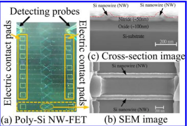
The poly-Si NWs with source and drain (S/D) contacts were then created using photolithography and plasma etching. The S/D contacts were estivated by a 2000 nm thick SiO2layer to prevent current leakage.18 Figure 1a shows our poly-Si NW
FETs and the electric contact pads in the orange line serve as sources and drains. Inside the orange dashed line is one of the NW-FET devices. In our measurement system, the signals from NW-FET device were collected by the two detecting probes. These two probes can be also easily moved to make different NW-FET measurements. Figure 1b shows the SEM top-view image of a poly-Si NW structure which is consisted of two parallel poly-Si NW of∼1600 nm length. The poly-Si NW-FET has two nanowires in each device; one of the NW is the dummy structure. The cross-section structure with NW-FET device is showed in Figure 1c.
In the NW-FET device, the current IS from the source terminal is based on the applied drain-to-source voltage VDS and modified by the applied gate voltage VGS. All the measurements of the poly-Si NW-FETs were under back-gating conditions in this study. Figure 2 shows ISversus VGS characteristics of a poly-Si NW-FET, for VDS= 0.1 V and VGS varying from −1 to 3 V with a 0.2 V step. The electrical
properties of the poly-Si NW-FET exhibit threshold voltage of Vth∼ 2.16 V, subthreshold slope of S ∼ 0.84 V/decade, and field effect mobility of μ ∼ 225 cm2/V s. Figure 3 shows I
S−VDS
curves for VGS varying from −2 to 3 V. The device exhibits typical metal-oxide-semiconductorfield effect transistor (MOS-FET) behavior, and the electronic properties of the poly-Si NW-FETs are well described by the conventional MOSFET theory. The experiments in this study reveal that current increases with increasing back-gate voltage VGSsuperposed on forward VDS in the NW-FET device. This characteristic also indicates the n-type-semiconductor nature of the device.
The measurement processes of the poly-Si NW-FETs were in an electromagnetic isolated probe station to reduce electro-magnetic interference. All experimental results were obtained with measurement system included a high-precision source measure unit (PXI-4132, National Instrument) and a low-noise current preamplifier (SR570, Stanford Research Systems). These measurements of electric properties of the poly-Si NW-FETs were performed in air (room temperature, 45% humidity) under well-controlled conditions.
■
RESULTS AND DISCUSSIONThe real-time responses of the source current (IS) of the poly-Si NW-FET was investigated in the atmosphere. The back-gate voltage VGS was stepped up from 0 to 2.5 V in 0.5 V increments, with each step lasting∼5 s. During the step lasting time interval, IS was measured by our measurement system. The results described that ISincreased in conjunction with VGS, as shown in Figure 4. When the VGS was 0.5 and 1 V, the original current (IDS) was lower than the peak current and the
Figure 1. (a) Poly-Si NW-FETs with detecting probes. Inside the regions defined by an orange solid line and dashed line are the electric contact pads and one NW-FET device, respectively. The nanowire region is circled expanded as shown in (b). Top-view SEM image of a poly-Si NW-FET with a 200 nm scale bar. Cross-section structure of a poly-Si NW-FET device shown in (c). The nitride layer is∼50 nm, and the oxide layer is∼100 nm.
Figure 2.Measurement of current ISwith the gate-source voltage VGS
switched from−1 to 3 V.
Figure 3.ISvs VDSmeasurement for various values of VGS.
Figure 4.Temporal response of ISas VGSis stepped up from 0 to 2.5 V
peak would be measured. As the VGSwas higher than 1.5 V, the original current (IDS) would cover the peak current and the IDS current would make main contribution to data measurement. However, the spike of ISwere observed for the VGSsteps from 0 to 0.5 V and from 0.5 to 1 V.
At the same time, the peaks of gate-to-source current (IGS) in response to switching VGSwere also monitored in Figure 5. The
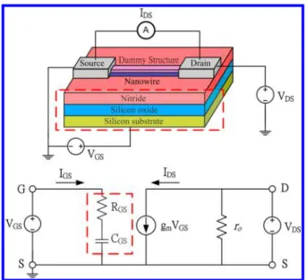
peak of IGScould be interpreted as minimal leakage current due to VGSthrough the dielectric interface to the drain and source channel. Furthermore, the minimal leakage ∼0.3 nA would cause ISbursting phenomenon at low gate voltage but would be stopped while gate voltage VGS up to 1.5 V. Although the leakage current from the back-gate voltage was covered for larger IS, this event can affect the accuracy of poly-Si NW-FET measurements for biosensing applications because ultrahigh sensitivity is dependent on small electronic signal measurement. The origin of this IDS spike has been attributed to be the charging effect of a capacitor because the structure between source and gate in the poly-Si NW-FET is similar to a capacitor. For interpreting the bursting phenomenon clearly, a physical model, an equivalent transformation model of electric circuit of a n-type NW-FET, is given in Figure 6, where G is back gate, D is drain, S is source, VGS is the back-gate voltage, RGS is the equivalent resistance, CGS is the equivalent capacitance, gm is the transconductance of the device, rois the output impedance, and VDSis the drain-to-source voltage. In the physical model, the drain-to-source current (IDS) can be described by the MOSFET theory as follows21−24
μ = ⎜⎛ ⎟ − ≈ ⎝ ⎞⎠ I C W L (V V V) g V n DS ox GS th DS m GS (1) where n is the charge-carrier effective mobility, W is the gate width, L is the gate length, Coxis the gate oxide capacitance of the NW-FET unit area, and Vthis the threshold voltage. The VGSwas applied to the Si substrate, which consisted of a silicon dioxide (SiO2) layer and a silicon nitride (Si3N4) layer. Although no leakage current IGS through the dielectric layers was expected, experimental results show that leakage current IGSwas nonzero during VGSswitching. Hence, these dielectric layers between source and gate can be described a simple series RC circuit. To analyze this equivalent circuit quantitatively, Kirchhoff’s loop rule is applied, and the response of IGS is expressed as = − I V R q R C GS GS GS GS GS (2)
where IGSis replaced by dq/dt. Then q(t) can be evaluated as
= − −
q t( ) V CGS GS{1 exp[ t/(R CGS GS)]} (3)
Then the current through the back gate substrate is obtained by
= − I t V R t R C ( ) exp[ /( )] GS GS GS GS GS (4) The source current IS(t) consists of two components. One is the leakage current IGS(t) produced by the charging effect of a capacitor, and the other one is the drain-source current (IDS) produced by the drain-to-source voltage (VDS). The source current can be expressed as
= + = − + I t I I V R t R C g V ( ) exp[ /( )] S GS DS GS GS GS GS m GS (5) This physical model indicates that current signal IS will be contaminated with leakage current IGS soon after VGS is switched on or changed. The measured current signal ISwould be dominated by real channel current between drain and source long after switching VGS. Typically, the efficiency of the leakage current would fade out while t≫ RGSCGS. Figure 7 shows that the experimental results are well reproduced by the simulation using the physical model outlined above; the correlation coefficient for the fit is ∼0.9354. The experimental results fitted with eq 4 were extracted RGS≈ 1.6 GΩ and CGS≈ 0.27 pF for VGS switching from 0 to 0.5 V and with VDS = 0.1 V. This physical model can therefore be used to explain the IS spike phenomenon for measurements done while switching VGS at low gate voltage.
According to previous discussions, the simplest method to avoid the interference of leakage current (IGS) is applying appropriate time lag before collecting ISdata in the biosensing
Figure 5.A comparison between ISand IGSafter VGSis switched from
0 to 0.5 V.
Figure 6.Equivalent circuit model of the NW-FET. RGSand CGSare
the equivalent resistance and capacitance in the proposed physical model for the back-gate NW-FET structure, which is boxed in the red dashed line in the schematic above the circuit diagram. G is back gate, D is drain, S is source, VGS is the back-gate voltage, gm is the
transconductance of the device, rois the output impedance, and VDSis
experiment. However, equivalent resistance and capacitance of the NW-FET will differ after semiconductor processing; determining the required time lag to reach stable state of IS becomes difficult. To avoid the charging effect of the capacitance in the NW-FET, the sloped-gate voltage method was used to the ISmeasurement in Figure 8. On the basis of eq
4, IGS is proportioned to VGS. In general, the VGS sweep was applied a step function in VGSswitching (dotted line in Figure 8). Here the step VGSin common use was modified as a sloped VGSchanging (solid line in Figure 8) to reduce the gate voltage different under Δt. Therefore, VGS was slowly stepped up to measure IS independently of VGS. The applied potential difference between the poly-Si NW-FET source and gate was sequentially increased VGSto the experimentally required value. NW-FET devices are usually used to detect biosignal variances in a liquid environment. Therefore, the experiments of IS measurement results compared without sloped-gate voltage method to with the method in PB (phosphate buffer, 10 mM) solution in Figure 9. After VGSwas switched from 0.2 to 0.4 V, the results shown in Figure 9a were acquired without adjusting the VGSslope m (step function), and Figure 9b shows results for IS with the slope adjusted to m = 0.04. The corresponding variancesσ of different operating conditions in IS are 1.12 × 10⁻¹⁰ and 1.783 × 10⁻¹¹, respectively. The corresponding variancesσ is defined by the standard deviation of the averaged ISto interpret the variance of measurement of IS. Theσ is represented by (6) as
∑
σ = −μ = N X 1 ( ) i N 1 time time (6) where∑
μ = = N X 1 i N 1 time (7) Time isfive different sampling points of time (1, 10, 100, 500, and 1000 ms). These results indicate that switching VGSwith an adjusted slope m permits simultaneous measurements of ISthat are unaffected by the leakage current IGS. The results of the variances for ISare summarized in Table 1.For the poly-Si NW-FET in air, the variance reduced almost 2 orders of magnitude upon using the sloped-gate voltage method. Under liquid (De Ion water, DI Water) conditions, the variance decreased slightly more than 1 order of magnitude. The variance decreased∼1 order of magnitude in PB solution. These data demonstrate that the sloped-gate voltage method can also be applied under liquid conditions, making it a promising technique for future in biosensing processing. In addition, the slope-gate voltage method on reproducibility has been shown in the Supporting Information.
■
CONCLUSIONNW-FET has become an import device in the area of biological sensing application. The detecting tiny amounts of charged biomolecules affect femtoampere (fA) to nanoampere (nA) current change of electrical characteristic. Experimental results show that the leakage current IGS is caused by the charging effect of an equivalent capacitor in the NW-FET structure. To explain this phenomenon, a physical model with equivalent resistance and capacitance was developed to simulate the leakage current of the poly-Si NW-FET, and thefit based on this model has a high correlation with the experimental data. This study also shows that the leakage current (IGS) affects the
Figure 7.Experimentally measured IGSfor VGSswitched from 0 to 0.5
V statefit (red line) with eq 4.
Figure 8.Slope modification used in VGSswitching from 0.2 to 0.4 V.
Figure 9.(a) ISmeasured at various times after switching VGSfrom 0.2
to 0.4 V without sloped-gate method in PB solution. (b) Same measurement as for (a) but with sloped-gate voltage method.
Table 1. Variance in MeasuredIDSValues (ampere) after SwitchingVGSwith and without AdjustingVGSSlope in Three Experiment Conditions
variance of IDS(A) with different time intervals
experiment condition without sloped VGS with sloped VGS
air 1.189× 10⁻¹⁰ 1.985× 10⁻¹² DI water 1.788× 10⁻¹⁰ 1.120× 10−10 PB 2.682× 10⁻¹¹ 1.783× 10⁻¹¹
accuracy of NW-FET measurements. To solve this problem, a novel VGSswitching method, which is the sloped-gate method, was proposed. The results indicate that the sloped-gate method decreases the variance in IDSmeasured after switching VGS, for poly-Si NW-FETs detections in air, liquid, and phosphate buffered solution (PBS). This method of measuring ISin NW-FETs can be used for accurate measurements of different targets or for other applications as part of a biosensor platform; on the other hand, the physical model is able to evaluate the equivalent capacitor in the NW-FET for other analysis parameters of the biosensing application.
■
ASSOCIATED CONTENT*
S Supporting InformationTable I. This material is available free of charge via the Internet at http://pubs.acs.org.
■
AUTHOR INFORMATIONCorresponding Author
*E-mail [email protected], Tel 886-3-5729287 (Y.-S.Y.); e-mail [email protected], Tel 886-3-5779911 (C.-H.H.).
Notes
The authors declare no competingfinancial interest.
■
ACKNOWLEDGMENTSThe NW-FET devices were prepared at National Nano Device Laboratories, National Applied Research Laboratories, Taiwan. We thank Professor Chii-Dong Chen of Academia Sinica, Taiwan, for helpful discussions. This work was supported by National Science Council (NSC101-2923-B-009-001-MY3 and 101-2622-B-009-001-CC1) and MOE-ATU Program.
■
REFERENCES(1) Cui, Y.; Duan, X.; Hu, J.; Lieber, C. M. Doping and Electrical Transport in Silicon Nanowires. J. Phys. Chem. B 2000, 104, 5213− 5216.
(2) Cui, Y.; Wei, Q.; Park, H.; Lieber, C. M. Functional Nanoscale Electronic Devices Assembled using Silicon Nanowire Building Blocks. Science 2001, 293, 1289−1292.
(3) Duan, X.; Huang, Y.; Cui, Y.; Wang, J. F.; Lieber, C. M. Indium Phosphide Nanowires as Building Blocks for Nanoscale Electronic and Optoelectronic Devices. Nature 2001, 409, 66−68.
(4) Huang, Y.; Duan, X.; Cui, Y.; Lauhon, L. J.; Kim, K. H.; Lieber, C. M. Logic Gates and Computation from Assembled Nanowire Building Blocks. Science 2001, 294, 1313−1317.
(5) Huang, Y.; Duan, X.; Cui, Y.; Lieber, C. M. Gallium Nitride Nanowire Nanodevices. Nano Lett. 2002, 2, 101−104.
(6) Duan, X.; Huang, Y.; Lieber, C. M. Nonvolatile Memory and Programmable Logic from Molecule-Gated Nanowires. Nano Lett. 2002, 2, 487−590.
(7) He, H., Jr.; Zhang, Yi Y.; Liu, J.; Moore, D.; Bao, G.; Wang, Z. L. ZnS/Silica Nanocable Field Effect Transistors as Biological and Chemical Nanosensors. J. Phys. Chem. C 2007, 111, 12152−12156.
(8) Varsano, D.; Garbesi, A.; Felice, R. D. Ab Initio Optical Absorption Spectra of Size-Expanded xDNA Bases. J. Phys. Chem. B 2007, 111, 14012−14021.
(9) Hsiao, C.-Y.; Lin, C.-H.; Hung, C.-H.; Su, C.-J.; Lo, Y.-R.; Lee, C.-C.; Lin, H.-C.; Ko, F.-H.; Huang, T.-Y.; Yang, Y.-S. Poly-silicon Nanowire Field Effect Transistor for Biosensing Application. Biosens. Bioelectron. 2009, 24, 1223−1229.
(10) Jones, P. A.; Baylin, S. B. The Epigenomics of Cancer. Cell 2007, 128, 683−692.
(11) Patolsky, F.; Timko, B. P.; Zheng, G. F.; Lieber, C. M. Nanowire-Based Nanoelectronic Devices in the Life Sciences. MRS Bull. 2007, 32, 142−149.
(12) Yang, M.; Qu, F.; Lu, Y.; He, Y.; Shen, G.; Yu, R. Platinum Nanowire Nanoelectrode Array for the Fabrication of Biosensors. Biomaterials 2006, 27, 5944−5950.
(13) Hahm, J.; Lieber, C. M. Direct Ultrasensitive Electrical Detection of DNA and DNA Sequence Variations Using Nanowire Nanosensors. Nano Lett. 2004, 4, 51−54.
(14) Lin, C.-H.; Hung, C.-H.; Hsiao, C.-Y.; Lin, H.-C.; Ko, F.-H.; Yang, Y.-S. Poly-Silicon Nanowire Field-Effect Transistor for Ultra-sensitive and Label-Free Detection of Pathogenic Avian Influenza DNA. Biosens. Bioelectron. 2009, 24, 3019−3024.
(15) Gao, X. P.; Zheng, G.; Lieber, C. M. Subthreshold Regime Has the Optimal Sensitivity for Nanowire FET Biosensors. Nano Lett. 2010, 10, 547−552.
(16) McAlpine, M. C.; Ahmad, H.; Wang, D.; Heath, J. R. Highly Ordered Nanowire Arrays on Plastic Substrates for Ultrasensitive Flexible Chemical Sensors. Nat. Mater. 2007, 6, 379−384.
(17) Stern, E.; Klemic, J. F.; Routenberg, D. A.; Wyrembak, P. N.; Turner-Evans, D. B.; Hamilton, A. D.; LaVan, D. A.; Fahmy, T. M.; Reed, M. A. Label-Free Immunodetection with CMOS-Compatible Semiconducting Nanowires. Nature 2007, 445, 519−522.
(18) Patolsky, F.; Zheng, G.; Hayden, O.; Lakadamyali, M.; Zhuang, X.; Lieber, C. M. Electrical Detection of Single Viruses. Proc. Natl. Acad. Sci. U. S. A. 2004, 101, 14017−14022.
(19) Lu, M.-P.; Hsiao, C.-Y.; Lai, W.-T.; Yang, Y.-S. Probing the Sensitivity of Nanowire-Based Biosensors Using Liquid-Gating. Nanotechnology 2010, 21, 425505−1−5.
(20) Lu, M.-P.; Hsiao, C.-Y.; Lo, P.-Y.; Wei, J.-H.; Yang, Y.-S.; Chen, M.-J. Semiconducting Single-Walled Carbon Nanotubes Exposed to Distilled Water and Aqueous Solution: Electrical Measurement and Theoretical Calculation. Appl. Phys. Lett. 2006, 88, 053114−1−3.
(21) Ishikawa, F. N.; Curreli, M.; Chang, H.-K.; Chen, P.-C.; Zhang, R.; Cote, R. J.; Thompson, M. E.; Zhou, C. A Calibration Method for Nanowire Biosensors to Suppress Device-to-Device Variation. ACS Nano 2009, 3, 3969−3976.
(22) Galup-Montoro, C.; Schneider, M. C. MOSFET Modeling for Circuit Analysis and Design; World Scientific: London, 2007.
(23) Malik, N. R. Electronic Circuits: Analysis, Simulation, and Design; Prentice Hall: Englewood Cliffs, NJ, 1995.
(24) Wang, J.; Gudiksen, M. S.; Duan, X.; Cui, Y.; Lieber, C. M. Highly Polarized Photoluminescence and Photodetection from Single Indium Phosphide Nanowires. Science 2001, 293, 1455−1457.