Stripe-geometry GaAs-InGaAs laser diode
with back-side contact on silicon by epitaxial
lift-off
J.C. Fan, K.Y. Chen,
Gray Liii and C.P. LeeIndexing terms: Semiconductor junction luxrs, Epituxiul lifi-of;f
The transfer of a preprocessed stripe-geometry GaAs-lnCaAs laser diode film onto a Pd/GePd coated n+-Si substrate is
reported with the backside contact on Si using epitaxial lifted-off
(ELO) technology. The Pd/Ge/Pd metal layers provide ohmic
contacts to both the Si substrate and the GaAs film, making
vertical conduction through the Si substrate possible. No device
degradation was observed after the EL0 process and comparable
results were obtained for the E L 0 laser diodes and the diodes
without the EL0 process.
The integration of semiconductor lasers with silicon electronic cir- cuits has always been a subject of great interest. This type of III- VlSi integration is important for applications such as optical com- munications and optical interconnections [I, 21. Many approaches including heteroepitaxial growth and material bonding techniques have been developed for this purpose [3 - 91. However, heteroepi-
taxial growth of GaAs laser diodes on Si suffers from a high dislo- cation density due to a large lattice mismatch. The poor material quality causes the lasers to degrade [lo]. Conversely, wafer bond- ing techniques such as bonding by atomic rearrangement [6] and epitaxial lifted-off (ELO) [S, 91 have the advantage of combining two different materials with different crystal structures.
Yablonovitch et ul. [9] and Pollentier et al. [8] have demon- strated E L 0 GaAs-AlGaAs broad-area lasers on a glass and an Si substrate. However, bonding a laser diode film on glass or a bare Si substrate by the Van der Waals force creates an insulating inter- face, which prohibits vertical conduction between the laser and the Si substrate. Hence, both the n- and p-type contacts must be fabri- cated on the front side of the grafted film. In this Letter, we describe an E L 0 technique for the fabrication of stripe-geometry lasers on an Si substrate with the backside contact on Si. Vertical conduction through the Si substrate was obtained and no device degradation was observed after the E L 0 process.
We have recently found that very good ohmic behaviour can be obtained between a GaAs thin film and an Si substrate if the ELO-GaAs film is grafted onto a Pd/Ge/Pd coated Si [I I]. This technique is applied here to fabricate an EL0 laser diode on Si. The strong metallurgical bonding between the GaAs thin film and the Si substrate also makes the facet cleavage possible without any danger of breaking the grafted film and the substrate.
The lasers used in this study were 980nm InGaAsIGaAs strained single quantum well lasers grown by MBE. The whole structure is the same as a conventional GRINSCH laser, except an
n-A1As sacrificd layer (lOOA thick, Si = 5 x 10'8cn~-') was grown between the laser structure and the substrate. Conventional ridge waveguide lasers with a 5 p n width were fabricated. The preproc- essed laser diodes on the GaAs substrate were covered with black wax on top and soaked in 10% H F solution to selectively remove the AlAs layer. The E L 0 film, after separation from the GaAs substrate, was dipped in HCl and H F before the bonding process.
A u B e SI0 2
clodding Layer
P d / G e / P d
N contact (AI)
'
Fig. 1 Siructuve o j oxide-defined E L 0 .stuipe-geometry lnGaAs/GuAs/ AIGuAs GRIN-SCH lasers diode OFZ n'-Si subsirute with backside con- tact on Si
The n+-(100) Si substrate (R = O.Ol-lC2cm) was used as the host substrate in the E L 0 process. A IOOOA PdI1300A Ge/2500A Pd metallic multilayer was deposited on the Si substrate by an elec- tron-gun deposition system under a base pressure of < 8 x 10⁻⁷
torr. After deposition, the Si substrate was lapped down to 1OOpn thick, and a 5000A thick
Al
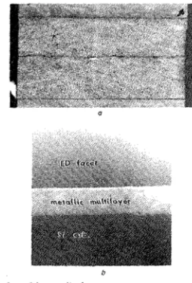
film was evaporated onto the back- side as the back side ohmic contact. The prepared 1 0 0 p thick a'- Si substrate with Pd/Ge/Pd metallic overlayer was then dipped in an H F solution. Finally, the E L 0 laser filmand the E'-Si sub- strate 'were bonded together by Van der Waals bonding. The bonded sample was heated in a fumace at 400°C for 30min under a forming gas ambient. No external pressure was needed during the heat treatment. Ohmic contacts were fonned at this stage both at the interface between the grafted film and the Si substrate and the backside of the substrate. As described in our previous work, the ohmic contact formed by PdiGePd provides a low resistance conduction path between the film and the substrate [ll]. The bonded sample was then cleaved into bars along the [11O] direc- tion. This metallurgical bonding at the interface provides enough strength for the facet cleavage process. A schematic diagram of the finished device is shown in Fig. 1.Fig.2 Phompiiphs of laser diode
a Top view photograph of E L 0 stripe-geometry InGaAsiGaAsl AlGaAs GRIN-SCH laser diode on n'-Si substrate after cleaved into
bars
b SEM photograph of cleaved facet of E L 0 laser diode
L o
T
3 0i
/ '/'
J
0 LO 80 120 input current, mAFig.3 Measured lighl-current churucteri.stic.s of' E L 0 laser on Si and laser O H GuAs without E L 0 process
Stripe width: 5 p I Cavity length: 8 O O p 1
- - -~ - as grown LDs . . . , . , . . E L 0 LDs
Fig. 2a shows the top view of a laser diode on Si after being cleaved into bars. Fig. 2b shows the SEM photograph of the
cleaved facet of a laser diode. From the photograph, we can clearly see the uniform and smooth bonding interface between the laser diode and the Si substrate. Fig. 3 shows the light-current characteristic of a bonded laser/silicon diode with a 8 0 0 p long cavity. The threshold current was 16.3mA and the slope efficiency was O.4WIA per facet without facet coating. For comparison, we
also include a light-current curve for a laser diode on GaAs sub- strate without the E L 0 process. The results are very similar between the two. To our knowledge, this is the first successful fab- rication of an E L 0 stripe-geometry laser diode on Si without per- formance degradation.
In summary, we have demonstrated an E L 0 stripe-geometry laser diode on an Si substrate with the backside contact on Si. The performance is simikar to that of a conventional laser diode on a GaAs substrate.
Ackno~c.ledg-,72ei~t~~: This work was supported by the National Sci- ence Council of the Republic of China under Contract No. NSC85-2215-E009-043.
0 1EE 1997
Electronics Letters Online No: 1997071 7
J.C. Fan, K.Y. Chen, Gray Lin and C.P. Lee (Department of
Electronic Eiigineering and Institute of Electronics, Nalional Chiao Tung University, Hsin-Chu, Tuiimn, Republic of Chinu)
22 April 1997
References
KOYANAG, M , TAKATA. H., MORI. H , and IBA, J . : ‘Design O f 4-bit X 4 layer optically coupled three-dimensional common memory for parallel processor system’, IEEE Solid-Stute Circuits, 1990, 25, pp. 109-1 16
FIAYASHI, I.: ‘Optoelectronic devices and material technologies for photoelectronic integrated systems’, Jprz. J. ,4ppl. Plzys., 1993, 32,
pp. 266-271
BRILLOUET. F : ‘First GaInAsP-lnP double-heterostructure laser emitting at 1.27pm on a silicon substrate’, Appl. Phys. Lett., 1988, 53, pp. 725-727
ACHEK. O , and B R 1 L L o u E - r . F : ‘First cw operation of a Ga,,,In,,,As, ,P, ,-InP laser on a silicon substrate’, Appl. Plzys.
Lett., 1988, 53, pp. 2389-2390
SUGO, M., MORI. H., TACHIKAWA, M., and ITOH. Y : ‘Room- temperature operation of an InGaAsP double-heterostructure laser emitting at 1 . 5 5 ~ on a Si substrate’, Appl. Phys. Lett., 1990, 57,
pp. 593-595
RAZEGHI, M , DEFOUK, M , O M N E S , E’., MAUREL, P H , CHAZELAS, J , and
RAZEGMI. M., D E F O U R , M , BLONDEAU, R., OMNES. F., MAUREL. P H ,
1.0, M Y , BNAT. R , HWANG, M.D., CHUA. C , and LJN, H . C :
’Semiconductor lasers o n Si substrates using the technology of bonding by atomic rearrangement’, Appl. Phys. Lett., 1993, 62, pp.
1038-1 040
WADA. I*., and KAMIJOH, T.: ‘Room-temperature cw operation of an InGaAsP lasers on a Si fabricated by wafer bonding’, IEEE Plzotonics. Technol. Letf , 1996, 8, pp. 173-175
‘Fabrication of a GaAs-AIGaAs GRIN-SCH SQW laser diode on silicon by epitaxial lift-off IEEE Photonics. Technol. Lett., 1991,
3 , pp. 115-117
‘Double heterostructure GaAsiAlGaAs thin film diode lasers on glass substrates’, IEEE Photonics. Technol. Lett., 1989, 1, pp, 41-
42
POLLENTIER. 1 , UUYDENS, L., VAN DAELE, P., and D E M E E S T E R , P.:
YABLANOVJTC‘H. E., KAPON, E . C M I T T E R , T.J , Y U N , C P , and RIIAT. R :
10 V A N D E R ZIEL, J P , DUPUIS. R . D , LOGAN, R A , and I’INZONE, C J :
‘Degradation of GaAs lasers grown by metalorganic chemical vapor deposition on Si substrates’, Appl. Pli,vs. Lett., 1987, 51, pp. 89-9 1
1 I F A N . J C , LEE, C P , CHEN, K.Y , and L I N , : ‘Epitaxially lifted-off n-
GaAs film onto PdlGeiPd coated Si substrate leading to vertical conduction across E L 0 film and Si substrate’, submitted to J.
Appl. Phys., I997
Threshold reduction of p t y p e &-doped
InGaAs/GaAs quantum
well
lasers
by
using
auto-doping of carbon
N . Hatori, A. Mizutani, N. Nishiyama, F. Koyama and K. Iga
Indexing terms: Semiconductor junction lasers, Semiconductor quuntuni wells
An InGaAsiGaAs quantum well laser using p-type &doping selectively in the barriers has been demonstrated to reduce the threshold current and carrier lifetime. A &doping technique is proposed, based on the experimental evidence of high density carbon inclusion during AlAs growth by metal organic chemical vapour deposition (MOCVD). A threshold current density as low as 160A/cm2 (54A/mz/well), has been obtained for three quantum well stripe lasers grown at 1.7 X 10‘*cm carbon doping.
InGaAsiGaAs quantum well (Qw) snrface-emitting lasers have been studied for optical interconnection due to their low threshold operation and low power consumption. In future parallel optical transmission systems under zero-bias modulation, it is important to reduce turn-on delay time [I, 21. For this purpose, it is desirable that the threshold current be < lOOpA for 1Gbitls. The carrier life- time should also be reduced further to obtain a decrease in turn- on delay time. There are already several reports on low threshold InGaAdAIGaAs or Al-free InGaAs edge emitting lasers [3 - 51.
To achieve its further reduction, modulation doped QWs [6, 71 are attractive, because the absorption determined byJ,( 1
-A),
where,/; and are the Fermi-Dirac distribution functions for the conduc- tion and valence bands, respectively, decreases whenbothA,
approaches 0 by p-type doping and,f; approaches I by n-type dop- ing. In particular, p-type modulation doped QW lasers have both larger gain and larger differential gain than conventional undoped QW lasers, resulting in a lower threshold operation and higher modulation bandwidth. Furthermore, it has been seen that the carrier lifetime is also reduced.C-doped A l A s ( l O &
InGaAs(80A):GaAs(lOOA) QWs
In
Fig. 1 Schematic band stmetnre o f active region using p-i.>’pe &doped AlAs layers
Not to scale
In this work, we propose a novel p-type &doping technique on InGaAsiGaAs QWs for low threshold operation, and have dem- onstrated threshold reduction in edge emitting lasers using the p- type &doped InGaAslGaAs QWs. We obtained a threshold cur- rent density of 160A/cm2 (< 54A/cm2/well) for three 1.7 x lO%m-’ 6-doped QWs edge-emitting lasers. Fig. 1 shows a schematic did- gram of the proposed st;ructure. The active region consists of three In, ,Gh ,As QWs of 80A thickness, separated by GaAs barriers of lOOA thickness. The carbon-doped p-type AlAs ( I O A) layers are located only around the centre of the barriers. We call the layers ‘6doped layers’. In each of the 10A thick AlAs layers, the carrier would be expected to flow by tunnelling. In this structure, we real- ised heavy carbon doping of the AlAs layers by only controlling the [As]/[Al] ratio in the growth. We call this technique, without additional dopant sources, ‘auto-doping’. We use AlAs layers as 6-
doped layers in this work since it is easy to dope carbon in AlAs layers by the auto-doping technique.
To realise this structure, the heavy doping of a less diffusing dopant is crucial. To achieve this, we grew an AlAs layer by