ELSEVIER Journal of Crystal Growth 160 (1996) 241-249
, . . . C R Y S T A L Q R O W T H
Structural and electrical properties of GaSb, A1GaSb and their
heterostructures grown on GaAs by metalorganic chemical vapor
deposition
Pai-Yong Wang, J.F. Chen *, W.K. Chen
Department of Electrophysics National Chaio Tung University, Hsinchu, Taiwan, R OCReceived 7 August 1995; accepted 28 September 1995
Abstract
A systematic study of structural and electrical properties of GaSb and AIGaSb grown on GaAs by metalorganic chemical vapor deposition is reported. In general, the results obtained from surface morphologies, X-ray linewidths and Hall properties are consistent with each other and indicate that the optimal growth conditions for GaSb are at 525°C around V / I l l = 1. A highest hole mobility of 652 cm2/V • s at RT (3208 cm2/V • s at 77 K) and a lowest concentration of 2.8 × 1016 cm-3 (1.2 × 1015 cm-3 at 77 K) were obtained for GaSb grown under this optimal condition. Compared to the GaSb growth, a smaller V / I l l ratio is needed for the AIGaSb growth to protect the surface morphology. When A1 was incorporated into GaSb growth, mobility decreased and carrier concentration increased sharply. The A1GaSb grown at 600°C had a background concentration about one order of magnitude lower than the AIGaSb grown at 680°C. Room-temperature current-voltage characteristics of GaSb/AlxGa l_xSb/GaSb show a rectifying feature when A1 composition x is higher than 0.3, suggesting a valence-band discontinuity at the AIGaSb/GaSb interface. A leakage current much higher than the value predicted by the thermionic emission theory is observed at 77 K, presumably due to a large number of dislocations generated by the huge lattice mismatch between GaSb and GaAs.
1. I n t r o d u c t i o n
Semiconductor I I I - V compounds containing Sb are promising materials for infrared, optical and high-speed devices in the spectral region from 1.3 to 6 . 5 / z m [1-3]. Moreover, GaSb has high hole mobil- ity [4] and therefore, is a good candidate for conduc- tive layers of p-channel field-effect transistors. These devices have usually been grown by liquid phase epitaxy or molecular beam epitaxy (MBE) with rela-
* Corresponding author.
tively little data available for growth o f AIGaSb by metalorganic chemical vapor deposition ( M O C V D ) [5-10].
Growth of smooth and high purity Sb compounds by M O C V D is more difficult presumably due to complex growth kinetics and impurities [9], which are normally present in gases in an M O C V D system. For example, Chidley et al. [9] found that both the crystallinity and electrical quality of M O C V D grown A1GaSb were limited by carbon contamination from TMAI material. Properties of A1GaSb will undoubt- edly affect the G a S b / A 1 G a S b interface quality and the properties of overgrown GaSb. To be able to 0022-0248/96/$15.00 © 1996 Elsevier Science B.V. All fights reserved
242 P.-Y. Wang et al./Journal of Crystal Growth 160 (1996) 241-249 grow high-quality bulk GaSb and AIGaSb layers is
imperative for the success of MOCVD GaSb/AI- GaSb technology. Despite some reports on the elec- trical properties of GaSb and A1GaSb [5-10], very little data is available on the details of variation with growth conditions. Therefore, we undertake MOCVD growth of GaSb and A1GaSb and characterize their structural and electrical properties by a Normarski optical microscope, double-crystal X-ray diffraction and Hall measurement to find their optimal growth conditions. To study the effect of the undoped A1- GaSb layer on the leakage current in devices, several
GaSb/AlxGa~_xSb/GaSb
heterostructures were grown on p+-GaAs substrates with different A1 com- positions. Current-voltage(I-V)
characteristics were used to see the current blocking capability of the A1GaSb layer and also to study the interface quality.2. Experimental procedure
The GaSb and A1GaSb layers were directly grown on Cr-doped semi-insulating GaAs(100) substrates
(a) (b) (c)
401zm
(d) (e)
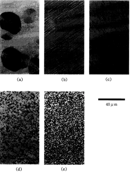
Fig. 1. The surface morphologies of the GaSb layers grown at (a) 500, (b) 525, (c) 550, (d) 575 and (e) 600°C with V / I I I = 1. It can be seen that the surface morphology is very sensitive to GaSb growth temperature. GaSb grown at 525 and 550°C had smooth morphology.
P.-Y. Wang et a l . / Journal o f Crystal Growth 160 (1996) 241-249 243
by the MOCVD system run at one atmosphere and has been discussed elsewhere [11]. We used TEGa, TMAI and TMSb sources. For studying the optimal growth conditions for GaSb, 1 /zm thick undoped GaSb was grown at a substrate temperature (T~) varying from 500 to 600°C with a V / I I I ratio kept at unity. Due to the low pressure of Sb, the V / I I I ratio was normally kept at a value not far away from unity. Next, T~ was fixed while varying the V / I I I ratio from 0.6 to 1.4. The growth rate of GaSb was kept at about 1 / x m / h . For growth of A1GaSb, T~
was varying from 600 to 680°C with V / I I I = 2. Several A1GaSb layers with different A1 composi- tions were grown to study the effect of the A1 composition on the layer quality. The AI composi- tion was determined by electron beam microprobe analysis after GaSb and A1Sb calibrations.
After bulk growths of GaSb and A1GaSb, GaSb/A1GaSb/GaSb (1.5 /zm undoped GaSb/0.2 /xm undoped A1GaSb/1 /zm undoped GaSb) het- erostructures with different A1 compositions were grown on p+-GaAs substrates. After growth, mesa
(a) (b) (c)
40pm
(d) (e)
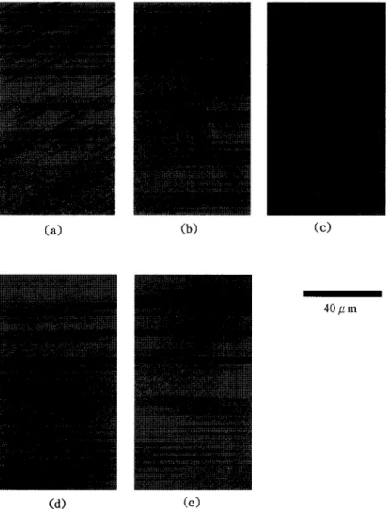
Fig. 2. The surface morphologies of the GaSb layers grown at 525°C with a. V / l l l ratio of (a) 0.6, (b) 0.8, (c) 1.0, (d) 1.2, (e) 1.4. No marked effect of the V / I l l ratio on GaSb mophology is noticed. This result shows that the GaSb layers grown at T s = 525°C had smooth surfaces irrespective of the values of the V / I I I ratio (0.6 to 1.4).
244 P.-Y. Wang et a l . / Journal of Crystal Growth 160 (1996) 241-249
diodes with an area of 7.06 × l 0 - 4 cm -z were made by evaporating A u - G e dots on top of the structures. The resulting devices were characterized for a leakage current at various temperatures be- tween 77 and 300 K.
3. Results
3.1. GaSb growth
To illustrate the effect of T~ on the surface mor- phology, we show in Fig. 1 GaSb grown at 500, 525, 550, 575 and 600°C with V / I l l = 1 (flow rate = 8.9 )< 10 -6 m o l / m i n ) . It can be seen that the surface morphology is very sensitive to T s. GaSb grown at 525 and 550°C had smooth morphology. T~ > 550°C, morphologies o f all the GaSb layers became rough. For 500°C growth, the surface showed three-dimen- sional cone-shaped structures, which were likely to be the result of a large sticking coefficient and a very low surface mobility o f Sb on the growth surface.
Keeping T~ at the optimal value o f 525°C, GaSb was grown with a V / I l l ratio from 0.6 to 1.4. Fig. 2 shows the resulting morphologies of the GaSb layers. We did not notice any marked effect of the V / I I I ratio on the GaSb morphology. V / I l l = 0.6 was sufficient to protect the GaSb surface grown at 525°C. This result showed that GaSb layers grown at T~ = 525°C had smooth surfaces irrespective of the values of the V / I l l ratio (0.6 to 1.4). However, V / I l l = 0.6 was not enough for GaSb if grown at 550°C. The grown surface became rough and puckers could be seen on it. The density of the surface puckers de- creased with increasing V / I l l ratio, and disappeared when the V / I l l ratio reached unity. This is expected since a higher V / I I 1 ratio is needed to protect the surface if grown at a higher temperature. Besides T~ and the V / I l l ratio, the absolute TMSb flow rate also affects the GaSb morphology. We found that at higher TMSb flow rate, GaSb with good morphology could be grown at higher T~.
The structural quality of GaSb on GaAs was examined by taking the (400) reflection from a dou- ble-crystal X-ray diffraction. Two peaks diffracted from two source signals can be resolved for the substrate and the epitaxial layer, which is indicative of high quality material. Fig. 3 shows the full width
800 • , • , • , 700 6 0 0 500 4 0 0 G a S b o n G a A s / /.
/
° i i 500 5 5 0 V/[II= l 300 450 600 650 TEMPERATURE (°C)Fig. 3. The full width at half maximum (FWHM) of X-ray diffraction for a 1 /xm thick GaSb layer grown at different temperatures under V/Ill = 1. A minimum FWHM of 360 aresec was observed for GaSb grown at 525°C and a sharp increase was seen for GaSb grown at T s > 550°C.
at half maximum ( F W H M ) for 1 /zm thick GaSb layers grown at different T~ under V / I l l = 1. A minimum F W H M of 360 arcsec was observed for GaSb grown at 525°C and a sharp increase was seen for GaSb grown at T~ ~ 550°C. The result that GaSb grown at 525°C has a minimum F W H M correlates well with the result of morphology. To illustrate the effect of the V / I l l ratio on the structural quality, we show in Fig. 4 the variation of F W H M for GaSb grown under different V / I l l ratios. For 525°C
700 6 0 0 ra 5 0 0 400 3 0 0 • , . , . , . , . , • GaSb on GaAs 5:25°C 2 0 0 . . . . 0 . 4 0 . 6 0 . 8 1.0 1.2 t . 4 1.6 V / I l l RATIO
Fig. 4. The variations o f the full width at half m a x i m u m ( F W H M ) o f X-ray diffraction for the G a S b layer g r o w n under different V / I l l ratios at a g r o w t h temperature o f 525 or 550°C. For 525°C growth, F W H M shows a m i n i m u m around V / I I I = 0.8 and I. For 550°C growth, the F W H M decreased with increasing V / H I ratio.
P.-Y. Wang et al./ Journal of Crystal Growth 160 (1996) 241-249 245
growth, FWHM shows a minimum around V / I I I = 0.8 and 1. For 550°C growth, FWHM decreased with increasing V / I I I ratio. These FWHM results are consistent with those o f surface morphologies.
Electrical properties o f GaSb on GaAs were char- acterized by Hall measurement at room temperature (RT) and 77 K. Unintentionally doped GaSb was all p-type. Fig. 5a and 5b show the growth temperature dependent properties of GaSb layers. A highest hole mobility of 652 c m 2 / V • s at RT (3208 c m 2 / V • s at
77 K) and a lowest concentration of 2.8 × 10¹⁶
cm -3 (1.2 × 1015 cm -3 at 77 K) were obtained for GaSb grown at 525°C under V / I I I = 1. This mobil- ity is comparable to the highest ever reported [9] by M O C V D and indicates a low level of impurity com-
10 4 E >. 10 3 o lO 2 1 0 1 7 i 10 *e 1015 , , .. .. , . .. . , • a G a S b on GaAs
o/° o
7 7 K • o~.~
OOK V / I l l = 1 • , ... . , . . . . , , 5 0 0 5 5 0 6 0 0 T E M P E R A T U R E (°C) b , , . . , . . . . , C a S b on G a A s / e / 3 0 0 k / " o ~ o / V / l l l = 1 5 0 0 5 5 0 6 0 0 TEMPERATURE (°C)Fig. 5. (a) Measured hole mobilities and (b) concentrations at 77 and 3 0 0 K as a function of GaSb growth temperature. The V / I l l ratio was kept at unity during the growth. A highest hole mobility of 6 5 2 c m 2 / V . s at RT ( 3 2 0 8 c m 2 / V . s at 77 K) and a lowest concentration o f 2 . 8 X 10¹⁶ c m - 3 ( l . 2 X 10¹⁵ c m - 3 at 77 K) were obtained for GaSb grown at 525°C under V / I l l = 1.
104 a • 525°C a ~ m 7 7 / ~ ~ u 5 5 0 O C ,.._..-~e 10 s : i 5 2 5 ° C A ... ~ ... a . . . ~ . . . 2 3 o 0 K O 5 5 0 O C • .... G a S b o n G a A s 102 . . . i i , i 0 . 4 0.6 0.8 1.0 1.2 1.4 .6 V/Ill RATIO 1017 5 5 0 o c . ° b • ' • . . . o . . - / • 5ZS°CA ... ~. 300K 5 5 0 O C , . . ~ " ... a. • .a'" / " x I
~ lO'" ~zs c-~.x ~.
• G a S b o n GaAs A / 0 . 4 0.6 0 . 8 1.0 1.2 1.4 1.6 V/III RATIOFig. 6. (a) Measured hole mobilities and (b) concentrations at 77 and 3 0 0 K as a function of V / I I I ratio. The GaSb layers were grown at 525 and 550°C, respectively. A weak dependence of mobility on the V / I I I ratio was observed. For the case of T s =
525°C, the highest mobilities and lowest concentrations were observed for V / I I I around 1.0 a n d 1.2.
pensation. Mobility at 77 K decreased sharply with either increasing or decreasing T, away from 525°C. For GaSb grown at 575 or 600°C, N A - N D at RT was even as high as 1017 cm -3. The lack of tempera- ture dependence of mobility between RT and 77 K for GaSb grown at 575 and 600°C suggests a high level of impurity compensation, thus background impurity or stoichiometric defect density may even be higher than shown. We also recorded the Hall data on GaSb grown at 525 and 550°C, respectively, as a function of V / I I I ratio. The results are shown in Fig. 6a for mobilities and Fig. 6b for hole concentra- tions. GaSb grown at 525°C has a higher mobility and lower hole concentration than GaSb grown at 550°C. The measured mobilities at 77 K show weak dependence on the V / I I I ratio. For the case of
246 P.-Y. Wang et al./Journal of Crystal Growth 160 (1996) 241-249 T~ = 525°C, highest mobilities and lowest concentra-
tions were observed for V / I l l around 1.0 and 1.2. While the surface morphology does not clearly show the effect of the V / I I I ratio, X-ray FWHM and Hall data clearly indicates that the optimal GaSb growth condition is at T~ = 525°C around V / I l l = 1. Be- sides this, the results from surface morphology, X-ray linewidth and Hall data are, in general, consistent with each other.
3.2. AIGaSb growth
Typical morphology of undoped A1GaSb on GaAs is mirror-like seen by the naked eye and is similar to or even slightly better than that of GaSb. Several
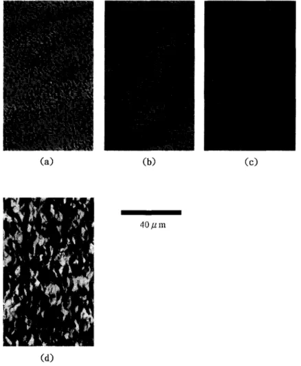
AlxGa~_xSb layers with different x were grown to study the effect of AI composition on surface mor- phology. Compared to the GaSb growth, we found that a small V / I l l ratio is needed for the AIGaSb growth to protect the surface morphology. Fig. 7 shows the morphologies of AlxGal _xSb with differ- ent A1 compositions directly grown on GaAs at 600°C. To illustrate that a reduced V / I I I ratio is needed for A1GaSb growth, we show in Fig. 7a a rough morphology of GaSb grown at 600°C under V / I I I = 2, due to the insufficiency of Sb to protect the grown surface. When A1 was incorporated into the growth, keeping the same Sb flow rate, the morphologies became smooth as Fig. 7b for x = 0.17 and Fig. 7c for x = 0.41 show. This clearly shows
(a) (b) (c)
4 0 ~ m
(d)
Fig. 7. The surface morphologi~ o! AlxGal_xSb with (a) x = 0, (b) x = 0.17, (c) x = 0.41, and (d) x = 0.58 Al composition. The AIxGa t _xSb was directly grown on the GaAs substrate at 600°C.
P.-Y. Wang et al./Journal of Crystal Growth 160 (1996) 241-249 247
10 3
-L c,/ c j 10 z E ©101
10 z°1019
I1018
v 101710 in
7 7 K ~ AlxGa I x Sb 300 ' 0 .... 771( • ... o . ~ . 3 0 0 K o " . . 6 0 0 ° C • • ~ o • ... • ^~^l:,~u°ua
L i i h 0.0 0.2 0.4 0.6 0.8 X , . , , o ~ ! 6 8 0 ° C 3 0 0 1 ( . . " • • " ? ? K" ?
o y a 6oo°c 3 0 0 K I I 0.0 0.2 AlxGa 1 xSb b I I 0.4 0.6 0.8 XFig. 8. (a) Measured hole mobilities and (b) concentrations at 77 and 300 K for A l x G a l _ x S b layers grown at 600 and 680°C, respectively, as a function of AI compositions x. AIGaSb grown at 600°C had a background concentration of about one order of magnitude lower than that of AIGaSb grown at 680°C.
primarily the dominating mechanism. Although their surface morphologies are similar, the electrical prop- erties of A1GaSb are much inferior to GaSb. We tried to grow A1GaSb at several different tempera- tures to see whether the background concentration could be reduced. However, the effect of varying the growth temperature to lower the background concen- tration is limited. The best result we obtained was for A1GaSb grown at 600°C. A typical result is shown in Fig. 8, where Hall data are compared for A1GaSb grown at 600 and 680°C (under V / I I I = 2). The AIGaSb grown at 600°C had a background concen- tration of about one order of magnitude lower than that of the AIGaSb grown at 680°C. However, their background concentrations were still higher than 1017 cm -3 and increased apparently with increasing A1 composition. A similar sharp increase of background concentration by the incorporation of even a small amount of aluminium had been previously reported [9], and is attributed to carbon contamination in the MOCVD growth. The A1GaSb growth using the new AI source is under investigation. Properties of A1- GaSb will affect the A1GaSb/GaSb interface quality and the properties of overgrown GaSb. To be able to grow a low background concentration for A1GaSb is imperative for M O C V D ' s applications in quantum- confined A1GaSb/GaSb heterostructures.
3.3. I - V characteristics of GaSb /A1GaSb / GaSb
SIFuctuFes
that the incorporation of a small amount of AI to GaSb can improve morphology. However, when A1 was increased to 0.58, the morphology became rough due to the insufficiency of Sb as shown in Fig. 7d. We also studied the effect of growth temperature on the surface morphology of AIGaSb. The morphology of AIGaSb grown at 600°C was found to be slightly better than that grown at 680°C under the same
v/In.
The electrical properties of undoped A1GaSb are shown in Fig. 8a for mobility and Fig. 8b for concen- tration as a function of A1 composition. Unintention- ally doped AlxGat_xSb is p-type. When A1 was incorporated into GaSb growth, mobility decreased and carrier concentration increased sharply. The lack of temperature dependence between RT and 77 K illustrates that the impurity or defect scattering are
The RT I - V characteristics of 1 /zm G a S b / 0 . 2
/zm AlxGa ~ _ x S b / G a S b structures in which undoped A1GaSb layers were grown at 600°C are shown in Fig. 9 for several A1 compositions. Voltages are measured with respect to the substrate. The whole structure was directly grown on the p+-GaAs sub- strate following the growth of a 1.5 /xm thick un- doped GaSb buffer layer. To see whether the inter- face between the p+-GaAs substrate and the p-GaSb buffer layer will have any effect on devices, an undoped GaSb layer was grown on the p+-GaAs substrate and measured the I - V characteristics. A
small ohmic resistance of 2 ~ , mainly due to mea- surement equipment, was observed, indicating that there is no noticeable potential barrier between them. Thus, the I - V characteristics shown in Fig. 9 are
248 P.-Y. Wang et al./Journal of Crystal Growth 160 (1996) 241-249
The AIGaSb layer is expected to behave as a barrier and the current should flow by thermionic emission over the A1GaSb layer. However, from the previous Hall data, we expect a high p-type back- ground doping for the A1GaSb layer. Thus, it is interesting to see whether the A1GaSb layer has any current blocking capability. Fig. 9 shows no appre- ciable barrier for x = 0 . 1 . For x = 0.3, the I - V
curve clearly shows a rectifying characteristic on both sides of the voltages. Since the high background concentration for 0.2 /zm thick A1GaSb, space- charge-limited current conduction can be ruled out for producing this rectifying feature. Therefore, Fig. 9 suggests that there is an appreciable valence-band discontinuity in the GaSb/A1GaSb interface. The G a S b / A I G a S b / G a S b structures have both normal and inverted A1GaSb/GaSb heterointerfaces, which govern the current conduction for positive and nega- tive voltages. The almost symmetrical feature of the
I - V characteristics in Fig. 9 indicates that both the normal and inverted A I G a S b / G a S b interfaces have comparable quality.
A valence-band offset of 0.4 _ 0.15 eV between AISb and GaSb was previously reported [12] by X-ray photoemission measurement. Expecting a lin- ear dependence of band discontinuity on the AI composition, we estimated valence-band discontinu- ities of 0.12 + 0.05 eV for x = 0.3 and 0.16 _ 0.06
0.06
0.04< •
0.02 [ - - 0.00 - 0 . 0 2 ~ . ) - 0 . 0 4-0.06
0.3 AI=O.I - 0 . 4 0.0 0.4 VOLTAGE (V)Fig. 9. Room-temperature current-voltage characteristics of
GaSb/AIxGal_xSb/GaSb structures with different AI composi- tions for the 0.2 Ixm thick AlxGa I _~Sb layer. The area of the mesa diodes is 7.06× l0 -4 cm -2. The whole structure was directly grown on the p+-GaAs substrate following the growth of a 1.5 /~m undoped GaSb buffer layer.
10 ° 10 -1 10 -z 10 -a ~- 10 -4 Z 10 -5
10 -e
I 0 -710 -s
0.6A
I
~
K
I i 0.0 0.2 0.4 VOLTAGE (V) c u r r e n t - v o l t a g e F i g . 10. T h e c h a r a c t e r i s t i c s o fGaSb/Alo.4Gao.6Sb/GaSb both at RT and 77 K. The area of the mesa diodes is 7.06 × 10⁻⁴ c m - 2 . The lack of temperature depen- dence on current is characteristic of defect or impurity-assisted tunneling.
eV for x = 0.4. These values should enable us to observe a rectifying feature in the I - V characteris- tics at RT. The results in Fig. 9 are consistent with this argument. Ideally, the current conduction is governed by thermionic theory. However, since the background concentration of A1GaSb could be higher than 1017 c m - 3 , thermionic field emission [13] is expected to play a part, especially in high-voltage current conduction. The increase of current with voltage in the high voltage range in Fig. 9 is possibly the consequence of this conduction.
Fig. 10 shows the I - V characteristics both at RT and 77 K for the case of x = 0.4. T h e result shows that the current at 77 K was about two orders of magnitude higher than the value predicted by the thermionic theory. Based on the theory [13], our calculation found that in an interesting voltage range < 0.5 V, thermionic emission is still the dominating conduction even for doping as high as 10 Is cm -3. The lack of temperature dependence on current is characteristic of defect or impurity-assisted tunnel- ing. This indicates that the AIGaSb contains a large density of defects or impurities. Dislocations gener- ated due to the large lattice mismatch between GaSb and GaAs substrates may be the main defects. These dislocations will extend to the GaSb/A1GaSb inter- face leading to the degradation of electrical proper- ties.
P.-Y. Wang et al./Journal of Crystal Growth 160 (1996) 241-249 249
4. Summary Acknowledgements
A systematic study o f structural and electrical properties of G a S b grown b y metalorganic chemical vapor deposition are reported. Surface morphologies o f G a S b are more strongly affected by the growth temperature while not by the V / I l l ratio (0.6 to 1.4). In general, the results obtained from surface mor- phologies, X-ray linewidths and Hall properties are consistent with each other and indicate that the opti- mal growth conditions for G a S b are at 525°C around V / I l l = 1. A highest hole mobility o f 652 c m 2 / V • s at R T (3208 c m 2 / V . s at 77 K) and a lowest concentration o f 2.8 × 10¹⁶ c m - 3 (1.2 x 10 ~5 cm -3 at 77 K) were obtained for G a S b grown under this optimal condition.
C o m p a r e d to the G a S b growth, a small V / I l l ratio is needed for the A1GaSb growth to protect the surface morphology. Unintentionally d o p e d A1GaSb is all p-type. W h e n A1 was incorporated into G a S b growth, mobility decreased and concentration in- creased sharply. The A1GaSb grown at 600°C had a b a c k g r o u n d concentration o f about one order of magnitude lower than that o f the A1GaSb grown at 680°C. However, their b a c k g r o u n d concentrations were still higher than 1017 c m -3.
Room-temperature c u r r e n t - v o l t a g e characteristics o f G a S b / A l x G a l _ x S b / G a S b show a rectifying fea- ture when AI c o m p o s i t i o n x is higher than 0.3, suggesting a valence-band discontinuity at the AI- G a S b / G a S b interface. A leakage current much higher than the value predicted by the thermionic emission theory is observed at 77 K, presumably due to a large amount o f dislocations generated by the huge lattice mismatch between G a S b and GaAs.
This work was supported in part by the National Science Council under contract no. NSC 84-2112- M009-021.
References
[1] D.C. Tran, G.H. Siegel, Jr. and B. Bendow, J. Lightwave Technol. (Special Issue on Low-Loss Fibers) LT-2 (1984) 536.
[2] S.J. Eglash and H.K. Choi, Appl. Phys. Lett. 57 (1990) 1292. [3] D.H. Chow, R.H. Miles, C.W. Nieh and T.C. McGill, J.
Crystal Growth 111 (1991) 683.
[4] J.F. Chen and A.Y. Cho, J. Appl. Phys. 70 (1991) 277. [5] H.M. Manasevit and K.L. Hess, J. Electrochem. Soc. 126
(1979) 2031.
[6] C.B. Cooper, R.P. Saxena and M.J. Ludowise, Electron. Lett. 16 (1980) 892.
[7] M. Leroux, A. Tromson-Carli, P. Gibart, C. Verie, C. Bernard and M.C. Sehouler, J. Crystal Growth 48 (1980) 367. [8] G.J. Bougnot, A.F. Foucaran, M. Marjan, D. Etienne, J.
Bougnot, F.M.H. Delannoy and F.M. Roumanille, J. Crystal Growth 77 (1986) 400.
[9] E.T.R. Chidley and S.K. Haywood, R.E. Mallard, N.J. Man- son, R.J. Nicholas, P.J. Walker and R.J. Warburton, J. Crys- tal Growth 93 (1988) 70.
[10] F.S. Juang, Y.K. Su, N.Y. Li and K.J. Gala, J. Appl. Phys 68 (1990) 6383.
[11] W.K. Chen, J. Ou and W.I. Lee, Jpn. J. Appl. Phys. 33 (1994) L402.
[12] J. Gualtieri, G.P. Schwartz, R.G. Nuzzo and W.A. Sunder, Appl. Phys. Lett. 49 (1986) 1037.
[13] C.R. Crowell and S.M. Sze, Solid-State Electron. 9 (1966) 1035.