國
立
交
通
大
學
資訊科學與工程研究所
碩
士
論
文
一個低延遲的全域非同步區域同步電路之界面
A Low Latency Globally-Asynchronous Locally-Synchronous Interface
研 究 生:陳崴哲
指導教授:陳昌居 教授
中 華 民 國 九 十 七 年 六 月
A Low Latency Globally-Asynchronous Locally-Synchronous Interface
研 究 生:陳崴哲 Student:Wei-Che Chen
指導教授:陳昌居 Advisor:Chang-Jiu Chen
國 立 交 通 大 學
資 訊 科 學 與 工 程 研 究 所
碩 士 論 文
A Thesis
Submitted to Institute of Computer Science and Engineering College of Computer Science
National Chiao Tung University in partial Fulfillment of the Requirements
for the Degree of Master
In
Computer Science June 2008
Hsinchu, Taiwan, Republic of China
一個低延遲的全域非同步區域同步電路之界面
研究生: 陳崴哲
指導教授:陳昌居教授
國立交通大學
資訊科學與工程學系碩士班
摘要
GALS藉由非同步的溝通方式,在模組之間提供了一個可靠的溝通方式,因此GALS 可被用在系統單晶片設計上。但是這種非同步的介面所造成的延遲可能會導致效能的減 少,因為當溝通發生時,並不會有任何的產出。因此如何減少GALS介面的延遲是很重 要的。 我們使用Verilog實作了一個更快,更小的可延伸時脈GALS介面,並且用TSMC 0.13 μm 元件庫做合成。最後,新設計的面積與速度會與其他設計做比較。同時,我們可在 模組與模組之間的資料傳輸路徑上多加一個先入先出的儲存元件,這可避免傳送端長時 間等待的情形。這些方法減少了模組間溝通的時間,GALS系統的效能也因此獲得提升。A Low Latency Globally-Asynchronous
Locally-Synchronous Interface
Student : Wei-Che Chen
Advisor : Dr. Chang-Jiu Chen
Department of Computer Science and Information Engineering
National Chiao-Tung University
Abstract
GALS can be used in SoC design because GALS provide a reliable communication by asynchronous channel between different modules. The latency of GALS interface is a problem which could cause performance degradation because there is no throughput when the communication occurs. Thus how to reduce the latency of GALS interface is significant.
A faster, smaller stretchable clock GALS interface is implemented with Verilog and synthesized with TSMC 0.13μm cell library. The area and speed of the new design are compared to other designs finally. Also a Muller-pipeline FIFO storage element can be added between the data transmission path to avoid long time waiting of sender. These schemes decrease the communication time of modules thus improve the performance of GALS system.
Acknowledgment
本論文能夠順利完成,首先要感謝陳昌居老師這兩年來的指導,以及口試委員鄭福 炯與范倫達老師的批評與指教。再來要感謝緯民、元騰以及宏岳學長對這篇論文提出的 建議,還有實驗室所有的同學及學弟們,陪我度過這兩年愉快的研究所時光。另外還要 感謝我的家人,讓我能安心完成學業,還有我可愛的魚兒們和吉他,讓我心靈能有所寄 託。這段期間大學及高中同學也給予我莫大的支持與鼓勵,謝謝你們。最後要感謝北大 門的土地公伯,保佑我能順利完成學業。Contents
摘要 ... I ABSTRACT ... II ACKNOWLEDGMENT ... III CONTENTS ... IV CHAPTER 1. INTRODUCTION ... 1 1.1SYNCHRONOUS CIRCUITS ... 1 1.2ASYNCHRONOUS CIRCUITS ... 1 1.2.1 Asynchronous Protocol ... 11.2.2 Asynchronous Data Encoding ... 3
1.2.3 C-element ... 5
1.2.4 Muller Pipeline ... 6
1.2.4 Pros and Cons of Asynchronous Circuits ... 7
1.3A NEW SOLUTION:GALS ... 7
1.4ORGANIZATION OF THE THESIS ... 8
CHAPTER 2. GALS ... 9
2.1OVERVIEW ... 9
2.2PAUSIBLE CLOCK ... 12
2.3GATED CLOCK ... 14
2.4STRETCHABLE CLOCK ... 16
2.5THE COMPARISON OF GALS CLOCKING SCHEMES ... 18
CHAPTER 3. THE PORT CONTROLLERS ... 20
3.1DATA TRANSFER IN GALS SYSTEM ... 20
3.2.1 The new STG ... 21
3.2.2 The timing constraint of the new STG ... 23
3.2.3 The new interface ... 23
3.3ADD FIFO BETWEEN MODULES ... 25
3.4THE LIMITATION OF STRETCHABLE CLOCK ... 26
3.5FUNCTION VERIFICATION ... 27
CHAPTER 4. IMPLEMENTATION ENVIRONMENT ... 29
4.1ENVIRONMENT ... 29
4.2C-ELEMENT IMPLEMENTATION ... 29
4.3OTHER PORT CONTROLLERS OF STRETCHABLE CLOCK GENERATOR ... 30
CHAPTER 5. THE RESULTS ... 33
5.1AREA REPORT ... 33
5.2TIMING REPORT ... 33
CHAPTER 6. CONCLUSION AND FUTURE WORK ... 35
List of Figures
Figure 1-1 : The sketch map of asynchronous system ... 2
Figure 1-2 : The four-phase handshake protocol ... 2
Figure 1-3 : The two-phase handshake protocol ... 3
Figure 1-4 : A GasP stage ... 3
Figure 1-5 : Dual-rail protocol... 4
Figure 1-6 : Transistor-level implementation of C-element ... 6
Figure 1-7 : Muller pipeline... 6
Figure 2-1 : The sketch map of GALS system ... 9
Figure 2-2 : The structure of GALS system ... 10
Figure 2-3 : quasi-synchronous transmission technique... 11
Figure 2-4 : The Pausible Clock based functional unit in a GALS system. ... 12
Figure 2-5 : The ring oscillator of pausible clock. ... 12
Figure 2-6 : The mutual exclusion element ... 13
Figure 2-7 : Timing diagram of output port controller ... 13
Figure 2-8 : The Pausible Clock based functional unit in a GALS system. ... 14
Figure 2-9 : The Pausible Clock based functional unit in a GALS system. ... 14
Figure 2-10 : timing graph of clock gating ... 15
Figure 2-11 : the local clock period decreases ... 16
Figure 2-12 : gate synchronizer ... 16
Figure 2-13 : Basic GALS structure with stretchable clock scheme ... 17
Figure 2-14 : the timing diagram of stretchable clock based GALS ... 17
Figure 2-15 : Stretchable clock generator ... 18
Figure 3-1 : Using a latch to register the data ... 20
Figure 3-3 : the STG of new stretchable clock GALS interface ... 22
Figure 3-4 : (a) new output controller, (b) new input controller ... 24
Figure 3-5 : sender waits receiver... 25
Figure 3-6 : FIFO between modules ... 26
Figure 3-7 : clock has to be stretched in the same clock cycle ... 27
Figure 3-8 : functional verification ... 28
Figure 3-9 : Verify with multiplier and adder ... 28
Figure 4-1 : gate-level simulation with ModelSim ... 29
Figure 4-2 : Gate-level implementation of C-element... 30
Figure 4-3 : Gate-level implementation of C-element with reset ... 30
Figure 4-4 : (a) Output controller, (b) Input controller with C-element ... 31
List of Tables
Table 1- 1 : Encode data with dual-rail encoding ... 4
Table 1- 2 : Encode data with 1-of-4 encoding ... 5
Table 1- 3 : the behavior of C-element ... 5
Table 1- 4: The pros and cons of asynchronous circuit ... 7
Table 5-1 : The area of each design ... 33
Table 5-2 : The area of FIFO ... 33
Chapter 1. Introduction
1.1 Synchronous Circuits
Most of the digital circuits nowadays are designed in synchronous method: using a global clock signal to control the data communication and behavior of circuits. This designing style has been prevalent in the area of digital circuits design in decades. The main reason is that synchronous circuits have many advantages as follows. Inherently, a synchronous system is controlled by a global clock signal. This makes the behavior of synchronous circuits is easier to be predicted than asynchronous ones. In addition, there are complete CAD tools to support the whole design flow of implementing synchronous circuits.
Nevertheless, synchronous circuits also have many disadvantages: As the complexity of circuits is increasing, the clock distribution and clock skew problems become troublesome. In the aspect of power consumption, for a synchronous circuit, lots part of power is dissipated by transition of the global clock signal. Taking DEC Alpha 21164 as an example, 40% of the chip power is consumed by the clock distribution network when the processor runs at its maximum speed [1]. Similarly, in the Motorola MCORE micro-RISC processor, the clock trees account for 36% of the total processor power [2]. Another downside is that the clock cycle time is bounded by the slowest component.
1.2 Asynchronous Circuits
1.2.1 Asynchronous Protocol
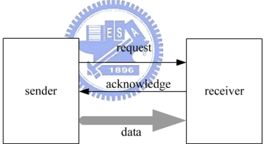
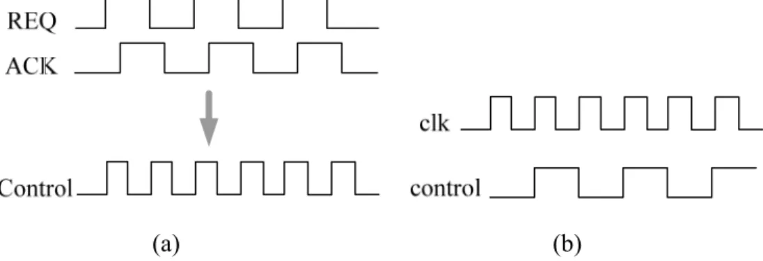
A simple asynchronous system is sketched in figure 1-1. The two most prevalent protocols used by asynchronous circuits are four-phase and two-phase. The four-phase protocol is shown in figure 1-2. When the data of the sender is ready, the sender lets req to logic 1. Once the request signal asserts, the receiver would acknowledge it by setting ack to logic 1. Finally,
req and ack are both reset to 0 therefore a handshake process completes.
The two-phase protocol is similar to the four-phase protocol however it has no “return-to–zero” process. When the sender is ready to send data, it changes the req (either 0Æ1 or 1Æ0), then the receiver acknowledge this by changing ack (either 0Æ1 or 1Æ0). After these two actions, a handshake process is completed. The major difference from the four-phase protocol is that the meaning of transition from high to low or low to high for req and ack are the same. The two-phase protocol is shown in figure 1-3.
Figure 1-1 : The sketch map of asynchronous system
Figure 1-2 : The four-phase handshake protocol
Figure 1-3 : The two-phase handshake protocol
Recently, some pulse-like asynchronous protocols are proposed. GasP [3] is one of these protocols. Figure 1-4 shows a single GasP stage. The request and acknowledge signals are combined in the same tri-state wire. This could shorten the cycle time because the characteristic of self resetting.
Figure 1-4 : A GasP stage
1.2.2 Asynchronous Data Encoding
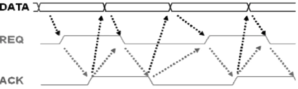
The term “Bundled-data” means that the data presentation is equal to the one in synchronous system. This way is closest to the data in synchronous circuits. Some data encoding mechanisms are useful for different purposes in designing asynchronous circuits. Dual-rail protocol encodes the request line in the data line. As table 1-1 shows, 1-bit data is
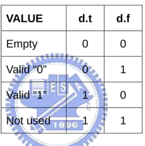
encoded with 2 wires called “d.t” and “d.f”. The codeword pattern {d.t , d,f} has totally four collocations: {0,1} and {1,0} mean the “valid” state of data and presents “logic 0” and “logic 1”, respectively. {0,0} presents the “empty” state which means that there is no valid data. In dual-rail encoding, the remaining pattern {1,1} is not used. In general, dual-rail protocol is very robust and thus can be used to achieve the goal of “delay-insensitive” which means that the gate and wire delays are “arbitrary”. In other word, the delay time of gate and wire make no effect on the correctness of circuits. The data transmission process with dual-rail protocol is depicted in figure 1-5. VALUE d.t d.f Empty 0 0 Valid “0” 0 1 Valid “1” 1 0 Not used 1 1
Table 1-1 : Encode data with dual-rail encoding
Figure 1-5 : Dual-rail protocol
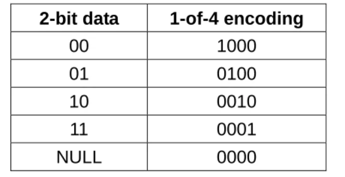
1-of-4 encoding, similar to the dual-rail one, is one of the one-hot encodings. In 1-of-4 encoding, 2-bit data is encoded into four wires, as table 1-2 shows. The advantage is that only half transition needed when a new data comes. In other word, only half power is consumed. In addition the one-hot encodings could be generalized to m-of-n encodings.
2-bit data 1-of-4 encoding 00 1000 01 0100 10 0010 11 0001 NULL 0000 Table 1-2 : Encode data with 1-of-4 encoding
1.2.3 C-element
C-element plays a significant role in asynchronous circuits design and is usually used to realize completion detection. The behavior of C-element, as shown in table 1-3, is similar to “AND” gate. The major difference between C-element and AND gate is that when two inputs is not equal, C-element will hold the preceding value of its output. A possible implementation of C-element in transistor-level is shown in figure 1-6.
in1 in2 out
0 0 0
0 1 No change
1 0 No change
1 1 1
Table 1-3 : the behavior of C-element
Figure 1-6 : Transistor-level implementation of C-element
1.2.4 Muller Pipeline
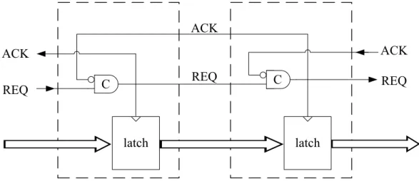
The 4-phase bundled-data pipeline, also known as Muller pipeline [4], is an elegant design in asynchronous field. Most of asynchronous pipelines are based on Muller pipeline. Figure 1-7 shows a 2-satge Muller pipeline which includes the control circuits and latches. This design is elegant because only one C-element and one inverter are used to be the control circuit of 1-stage Muller pipeline. According to the behavior of C-element, as the left circuit generates request to the right one but the right one is not ready to acknowledge it, the pipeline will eventually fill. Thus the Muller pipeline can be used as an asynchronous FIFO.
C REQ latch ACK ACK REQ C ACK REQ latch
1.2.4 Pros and Cons of Asynchronous Circuits
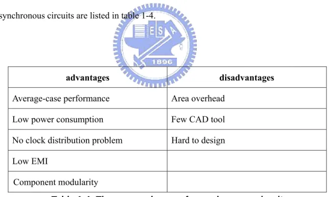
Inherently, asynchronous circuits have many advantages over synchronous ones [4]. First, considering the delay of both models, asynchronous circuits give the "average-case" performance compared to the "worst-case" in synchronous ones. Second, since the global clock signal doesn't exist in asynchronous designs, there is no power consumption dealing with the clock distribution which also means asynchronous circuits would have almost no power dissipation when it is idle. Third, asynchronous design has low EMI (Electromagnetic Influence). However, asynchronous circuits also have some disadvantages such as the area overhead for handshake circuits and lack of CAD tool to design, verify and test. Moreover, asynchronous circuits could bring the unpredictability of behavior. The pros and cons of asynchronous circuits are listed in table 1-4.
advantages disadvantages
Average-case performance Area overhead
Low power consumption Few CAD tool
No clock distribution problem Hard to design
Low EMI
Component modularity
Table 1-4: The pros and cons of asynchronous circuit
1.3 A new solution: GALS
distribution problem must be treated seriously. Hence a system using solely synchronous design can be controversial. GALS (Globally-Asynchronous Locally-Synchronous) methodology provides a reliable way to communicate between modules. The major characteristic of GALS is that the main modules of a chip are designed with synchronous method and the communication interface between locally-synchronous modules is completely asynchronous. GALS also offers a solution for SOC (system on chip) design for reliable communication and low power consumption.
1.4
Organization of the thesis
The GALS technology is introduced in chapter 2. In chapter 3, the new GALS interface is proposed. The implementation environment and tools are described in chapter 4. In chapter 5, the area and communication latency is showed. Finally, the thesis is concluded in chapter 6.
Chapter 2. GALS
2.1 Overview
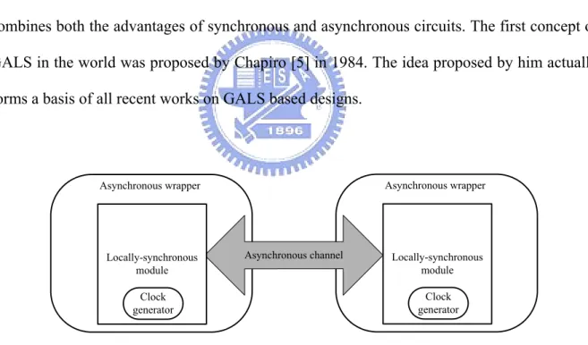
Synchronous circuits have some defects, such as the clock distribution and clock skew problems. As the die size increases, these problems become much more serious. Although asynchronous methodology has some disadvantages such as the area overhead caused by handshaking circuits and the lack of CAD tools for designing asynchronous circuits, it has the ability of resolving the problems arising from the clock and has some inherent advantages such as lower power consumption and average-case performance. GALS methodology combines both the advantages of synchronous and asynchronous circuits. The first concept of GALS in the world was proposed by Chapiro [5] in 1984. The idea proposed by him actually forms a basis of all recent works on GALS based designs.
Locally-synchronous module Asynchronous wrapper Clock generator Asynchronous channel Locally-synchronous module Asynchronous wrapper Clock generator
Figure 2-1 : The sketch map of GALS system
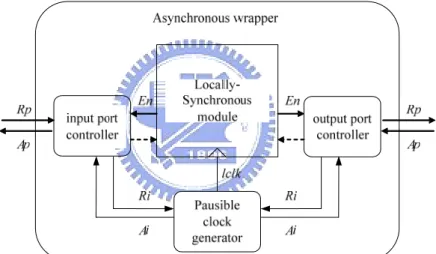
In a digital system, there must be several modules. By using the GALS methodology, all the modules are designed by traditional synchronous way and are encapsulated within an asynchronous wrapper. The clock generator is specially designed for GALS system. The communication interface between modules is purely asynchronous. As figure 2-1 depicts,
each synchronous module has its own clock generator. This means that each module could adopt its most suitable clock frequency to fit different functions of each module.
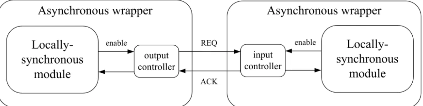
output controller Locally-synchronous module input controller Locally-synchronous module REQ ACK enable enable
Asynchronous wrapper Asynchronous wrapper
Figure 2-2 : The structure of GALS system
The basic structure of GALS system is shown in figure 2-2. The asynchronous interface has two major parts: input controller and output controller. The basic behavior of a GALS interface is as follows:
‧ When the sender wants to transfer data, it enables the output controller by an enable signal. Then the output controller advises the clock generator in some way and then the clock of synchronous module will be stopped. While the receiver needs to receive data, it will enable the input controller as well as the sender and the clock of receiver will be stopped subsequently.
‧ The output controller sends a request to input controller, and the input controller
acknowledge it only if the receiver needs data.
‧ After the handshake completes, the output and input controller will notify each
associative clock generator. Afterward the two synchronous modules continue to operate.
ensure the correctness of a system. This idea can be realized with a special clock generator. The detail implementation will be introduced later. GALS has large penalty on communication time [6]; hence the latency of asynchronous interface is significant for the system performance. The communication delay is significantly based on the design of port controllers. Thus, implement a simple and faster port controller is very important.
Another similar scheme used for data transmission between modules with different clock rates is called quasi-synchronous transmission technique [7]. In this scheme, REQ and ACK are replaced by a single control line, as figure 2-3(a) shows. This control line is generated by the clock source of transmitter and it is level transitive, as figure 2-3(b) shows. A mutual exclusion unit is used to stop clock rate for correct data transmission. Also, the proportion of clock rates of transmitter and receiver is determined by the flow control unit and after this process the rate of the control line will be determined. Although this methodology provides another way for communication between components with different operating rates, it is not a real asynchronous technique. Also, some additional hardware units such as flow control unit and phase frequency detector are needed. This renders the hardware cost may be larger than the cost of port controller in GALS system.
(a) (b)
Figure 2-3 : quasi-synchronous transmission technique
2.2 Pausible clock
Pausible clock generator, also called stoppable clock generator, was invented by Yun et al. in 1996 [8]. It is the most commonly used approach in designing GALS system so far. Figure 2-4 depicts a pausible clock based functional unit in a GALS system. In a pausible clock based GALS system, a ring oscillator is used to generate the local clock signal of the locally synchronous module, it uses odd number of inverters which is shown in figure 2-5. Ri is 0 since there is no data to transfer or to receive therefore rclk could be granted by the mutual exclusion element, as shown in figure 2-6, such that the clock can operate normally.
Figure 2-4 : The Pausible Clock based functional unit in a GALS system.
Figure 2-5 : The ring oscillator of pausible clock.
Figure 2-6 : The mutual exclusion element
When the LS (Locally-Synchronous) module needs to transfer or receive data, the clock should be paused so that the LS module will generate an enable signal En to advise the port controller. Afterward the port controller sends a request signal Ri to the pausible clock generator. The mutual exclusion element will grant it by the acknowledge signal Ai and the clock will be paused at the low phase. Then the data transmission process will be started. The actions of output port controller are depicted in timing diagram form in figure 2-7.
Ap Rp lclk gate gate elclk g g Data Data En En Locally-Synchronous module input port output port Clock gating asynchronous wrapper Gate Synchronizer Gate Synchronizer
Figure 2-8 : The Gated Clock based functional unit in a GALS system.
2.3 Gated clock
Clock gating is widely used in all synchronous system to save the power consumption but it worsen the clock skew problem. Apply clock gating on GALS system is adaptable because of the features of GALS. The clocking gating based GALS architecture is shown as figure 2-8 [9].
The clock generator of gated clock based GALS system is shown in figure 2-9. The clock generator of gated clock based GALS system is usual. The AND gate has one eclk input and may have many gate-signal inputs; because a GALS module could have many ports instead of only one port. When LS module needs data from other LS module, one of these
gate signals will go down thus the clock is gated. LS module enable data port controllers by
generating En signal at the negative edge of the clock pulse. The timing diagram of the clock gating is shown in figure 2-10. Let’s make some definition as follows, tand: the AND gate
delay, ttff: the T-flip flop delay, tpc: the port controller delay, tgs: the gate synchronizer delay.
Before the next rising edge of eclk the gate signal must be generated to guarantee the LS module catch the correct data. Therefore tand+ttff+tpc+tgs must < teclk/2.
Figure 2-10 : timing graph of clock gating
As shown in figure 2-11, it’s not allowed to release the clock at the high phase of eclk signal because it will decrease the lclk period [9]. Therefore the gate synchronizer should be designed to associate with eclk signal and the output of port controller (i.e. g signal). The implementation of gate synchronizer is depicted as figure 2-12.
Figure 2-11 : the local clock period decreases
Figure 2-12 : gate synchronizer
2.4 Stretchable clock
Another scheme of the clock generator applied in GALS system is stretchable clock. The notion of the stretchable clock generator is similar to the pausible clock generator: stop the clock when data transfer occurs. The major difference between them is the way to stop the clock. Pausible clock scheme uses a mutual exclusion element to choose clk signal or request signal to grant. However the stretchable clock generator simply uses a stretch signal to control the clock generator. Figure 2-13 shows a basic GALS structure with stretchable clock scheme. The timing diagram is shown in figure 2-14.
Figure 2-13 : Basic GALS structure with stretchable clock scheme
Figure 2-14 : the timing diagram of stretchable clock based GALS
One possible implementation of stretchable clock generator is shown in figure 2-15. It is only composed of one NOR gate, one C-element gate and odd number of inverters [10]. According to the behaviors of C-element described in chapter 1, it’s easily to find the behavior of the clock generator. When stretch is zero, the output of the NOR gate is determined by clk. If clk is logic 1 then the output of NOR gate will be logic 0. Through a C-element, logic 0 and the inverse of clk (i.e. logic 0, too) will outputs logic 0. Afterward, the output of NOR gate will become logic 1. The inverse of clk will also be logic 1 thus the
output of C-element will be logic 1, repeatedly. Only if stretch is asserted to high, the clock will be stopped. This is because the output of NOR gate is held at logic 0 and the output of C-element is held at logic 0, too.
Figure 2-15 : Stretchable clock generator
2.5 The comparison of GALS clocking schemes
Ring oscillator has some disadvantages [11]. Unlike crystal oscillator, the clock signal which is generated by ring oscillator is not stable. Furthermore, the clock frequency may be significantly influenced by temperature and voltage. Thus pausible clocking seems to be not suitable in designing high-performance GALS system which needs stable, low-jitter clock signal. The disadvantage of gated clocking GALS is that it is suitable in single-clock SoCs, not multiple-clock ones [9]. Most of the GALS design was implemented with pausible GALS methodology to date but it has some disadvantages. First, the clock generator and port controllers are more complex than stretchable clock based ones. Second, the mutual exclusion element takes the “toss a coin” strategy [12] (i.e. randomly), the pausible clock scheme could be metastable when the request and the rising edge of the clock arrive at the same time. From
stretch = 0 : clock runs stretch = 1 : clock stops
now on, there is no proper solution on current FPGA technique [13]. Furthermore, stretchable clock generator only simply uses a stretch signal to control the operation of clock. This thesis will focus on cell-based VLSI design flow instead of full-custom one; as a whole, the thesis will focus on the implementation of port controllers of stretchable clock scheme.
Chapter 3. The port controllers
3.1 Data transfer in GALS system
Although the clock will be restored after the communication cycle, it’s hard to know precisely that when the next clock positive edge will rise. Adding a latch on the interface to register the transmitted data is feasible. This scheme may avoid the data misses; thus it can ensure the correctness of data transmission [12]. In general, the latch is controlled by the ACK between the two port controllers, as shown in figure 3-1. The reason to take ACK as the latch control is that ACK can be asserted only if the output controller sends a request to input controller and the receiver also needs to get data. The latch is transparent if the receiver doesn’t switch to clock stretch mode. In other words, the latch is open such that it can’t hold the data until ACK is high.
Figure 3-2 : the STG of stretchable clock GALS interface
3.2 The new port controllers
3.2.1 The new STG
As shown in figure 2-6, a GALS unit using stretchable clock scheme has two port controller: input controller and output controller. For output controller, there are two input terminals: enable (WR, which means “write”) from locally-synchronous module and ACK from output controller, and two output terminals: REQ to output controller and stretch to local clock generator. Similarly, the input controller also has two input and two output terminals which are enable (RD, which means “read”), REQ, ACK, stretch. The most intuitive signal transition graph (STG) of stretchable clock based GALS interface is showed in figure 3-2. As the figure depicts, the STG starts after either input or output port controller is enabled by its individual LS module. After both two port controllers are enabled and the stretch signals are asserted, the handshake process is fired up. Finally, after the actions of handshake over the two stretch signals are de-asserted.
From the original STG, it can be seen that the clock of LS module starts again only after the handshake process is over. If the STG can be modified to make some signals transit in parallel, the less time will be wasted on the communication of two LS modules and further improve the system performance.
Figure 3-3 : the STG of new stretchable clock GALS interface
Based on the notion described above, a new STG is created as shown in figure 3-3. “ACK+” is the earliest point to start the parallel transitions. The reason to choose “ACK+” for the starting point of parallel transition is that when the STG goes to “ACK+”, it means sender wants to send data and also receiver wants to receive data. If we take the precedent point of “ACK+” in STG, that is, “REQ+”, for the beginning point, it may cause wrong data transmission. Let’s consider this condition: sender enables its own output controller and
asserts REQ subsequently Æ stretch is reset to zero Æ the clock of sender runs (sender may produce new data to transfer again thus old data is replaced by new one). But receiver doesn’t receive the old data yet such that data correction is violated. As a whole, it’s demonstrated that
“ACK+” is the earliest starting point for parallel signal transition.
3.2.2 The timing constraint of the new STG
The new STG must have two constraints to make sure the GALS system operates correctly. First, stretch- will make the clock restore again. If the rising edge of clock comes before ACK-, the wrong data may be latched in the latch which is controlled by ACK. Thus the time from ACK+ Æ ACK- has to be shorter than ACK+ Æ stretch- Æ clock restores. The second constraint is that the data has to be latched correctly during ACK+ Æ ACK- because the latch is controlled by ACK. If the timing consumption is not matched, several inverters could be added to delay some signals to fit the correctness. For example, if the interval from
ACK+ to ACK- is too short for latch to hold data stably, even number of inverters will be
added on this path for matching delay. Adding inverters or not for matching the constraints is depending on the design of port controllers. In our design, as shown in figure 3-4, no inverter should be added and the function correctness is ensured.
3.2.3 The new interface
The new input and output port controller, as shown in figure 3-4 (a) and (b), are implemented and verified. The behaviors are described below:
For the output controller:
‧ Initially, WR, stretch, REQ and ACK are all logic 0.
triggered and pulls up stretch next.
‧ After stretch becomes logic 1, REQ is generated and sent to the input port controller. ‧ The output controller waits for ACK from input controller. After ACK is received, the
output controller resets REQ and the D-FF (de-asserts stretch) simultaneously. ‧ After stretch is 0, the clock of sender is restored.
Q Q SET CLR D WR REQ ACK stretch VDD (a) (b)
Figure 3-4 : (a) new output controller, (b) new input controller
These processes of two port controllers described above are agreeable to the new STG in figure 3-3. As ACK is asserted, REQ and two stretch signals are reset in parallel. Conceptually,
the two port controllers indeed satisfy the requirement of decreasing communication latency of asynchronous interface.
Figure 3-1 shows that a latch is added for the purpose of reliable data transmission. The latch is controlled by ACK thus data has to be stored correctly in the latch in the time from
ACK+ to ACK-. From the simulation waveform, it can be demonstrated that data is stored
correctly thus the GALS system which operates with our new interface is reliable.
3.3 Add FIFO between modules
When the sender is going to transfer data but the corresponding receiver is not ready to receive data, as figure 3-5 depicts, the sender may waits for receiver to complete its own computation. There is no any computation in sender because of waiting for acknowledge from the input controller of receiver. This could cause performance degradation.
If we put a First-In-First-Out (FIFO) storage element along the transmission path as figure 3-6 shows, the sender could put the data into the FIFOs and get acknowledge early. Thus sender will continue computation instead of waiting for receiver. The 4-phase bundled-data FIFO structure is used, as figure 1-4 shows, which is famously known as Muller-pipeline. Note that the numbers of stage have to be even. This is because the Muller-pipeline only could hold half stage numbers of data when the FIFOs are full.
output controller input controller REQ ACK WR RD stretch stretch
LS
LS
F I F O REQ ACKFigure 3-6 : FIFO between modules
3.4 The limitation of stretchable clock
To make the GALS system operates correctly, when the stretch is asserted, the clock has to be stretched or stopped in the same clock cycle. If the clock is stretched after the next rising edge, error could occur. Figure 3-7 shows this situation. The clock rate produced from the stretchable clock generator depends on the number of inverter in figure 2-15. As the stretch
signal is asserted, the output of NOR gate will be 0 to keep the output of C-element at 0. If the number of inverters is too few, the inverse of clk signal ( i.e. high) will go to the input terminal of C-element earlier than the output of NOR gate. Because clock rises to stretch rises occupies some delay time, stretch may be late for rising. Therefore the C-element will output 1 because both its inputs are 1. As a whole, the number of inverters should be enough to ensure the correctness. According to the gate-level simulation waveform, the fastest clock rate of the clock generated by the stretchable clock generator is about 650 MHz with TSMC 0.13 μm cell library.
Figure 3-7 : clock has to be stretched in the same clock cycle
3.5 Function Verification
To verify the function correctness of our design, three relations of clock rates of receiver and sender are simulated in gate-level with ModelSim. The three cases are shown in figure 3-8. The sender sends a number per two clocks and the receiver receives it per two clocks too. In the gate-level simulation waveform, it’s demonstrated that the new interface indeed provide a reliable communication between two synchronous modules which have different clock rates. Further, a sender with an 8-bit multiplication function and a receiver with an 8-bit addition function are implemented with different clock rates for verification. These two functions are also exchanged to each other to verify function correctness. The simulation waveforms are shown in figure 3-9.
(a) clk sender = 555 MHz, clk receiver = 133 MHz
(b) clk sender = 555 MHz, clk receiver = 555 MHz
(c) clk sender = 133 MHz, clk receiver = 555 MHz
Figure 3-8 : functional verification
(a)
(b)
Figure 3-9 : modules with multiplication and addition function: (a) clk sender = 300 MHz, clk receiver = 400 MHz;
Chapter 4. Implementation Environment
4.1 Environment
The designs are implemented with gate-level coding style in Verilog hardware description language. Synopsys Design Complier Z-2007.03-SP3 is used to synthesize our gate-level design with TSMC 0.13μm cell library. The correctness is verified with gate-level simulation with ModelSim 6.0.
Figure 4-1 : gate-level simulation with ModelSim
4.2 C-element implementation
In this thesis, all C-elements are implemented in gate-level instead of transistor level. The transistor-level of C-element has been shown in chapter 1. The gate-level implementations of C-element and C-element with reset function are shown in figure 4-2 and figure 4-3.
Figure 4-2 : Gate-level implementation of C-element
Figure 4-3 : Gate-level implementation of C-element with reset
4.3 Other port controllers of stretchable clock generator
Two kinds of port controllers which were proposed in [10] are implemented in this thesis. The first kind of design is based on C-element, as figure 4-4 (a) and (b) draws. The other one, which are showed in figure 4-5 (a) and (b), is using standard cell such as D-FF and latch. The
area and performance will be listed and compared to our new port controllers in section 5. (a) (b)
Figure 4-4 : (a) Output controller, (b) Input controller with C-element Q Q SET CLR D Q Q SET CLR D L VDD WR stretch REQ ACK (a)
(b)
Figure 4-5 : (a) Output controller, (b) Input controller with standard cell
Chapter 5. The Results
5.1 Area Report
The area of each design is shown in table 5-1. It is based on TSMC 0.13μm cell library. The unit of area is μm2. The area of Muller-pipeline FIFO (only control circuits, not include latch) is listed in table 5-2. The C-element based design is very large because the C-element is implemented in gate-level. For giving the initial value “0” for some output of C-element, every C-element has the reset function, as shown in figure 4-3. If the C-element is implemented with transistor level, the area will be smaller. The standard cell based design has totally two Flip-Flops, two Latches with reset, two AND gates, two inverters and several inverters used to realize the matching delay. The new design merely has two Flip-Flops, two AND gates and one inverters. Obviously, the new design is much smaller than the standard cell based one.
C-element based Standard cell based New design
Area (μm2) 363.2 176.5 112
Table 5-1 : The area of each design
2-stage FIFO 4-stage FIFO
Area (μm2) 130.7 276.7
Table 5-2 : The area of FIFO
5.2 Timing Report
system, the time that when WR or RD rises are unpredictable (i.e. one of WR and RD may rises first and not at the same time). For fairness and simplicity, we assume that WR and RD arrive at the same time and take it as the starting time. The ending time is determined by the time that either stretch1 or stretch2 is reset later than the other one. The unit of time is ps. The results shows that the new design is much faster than the other two designs.
C-element based Standard cell based New design
time (ps) 3169 2290 1260
Table 5-3 : The latency of interface
Chapter 6. Conclusion and Future Work
A new GALS interface is proposed in this thesis. The interface includes a input controller and a output controller. Compared to the C-element based design, the area of our new interface is 30.8% and the communication time is 39.7%. Compared to the standard cell based design, the area is 63.5% and the communication time is 55%. The latency of GALS interface is reduced and the correctness of data transmission is ensured. Another way to reduce the latency is to add a Muller-pipeline FIFO between the modules. This can reduce the possibility that sender waits for receiver to receive data for a long time.
In our design, when receiver is ready to receive data but the sender is not yet ready to send data, the receiver will wait for sender for an unknown time. If receiver has other tasks to complete, this situation will degrade the performance. Thus the port controller has to be modified to make clock of receiver operates normally instead of being stopped if the data of sender is not ready.
In this thesis, the interface is based on four-phase handshake protocol. Because the interface proposed above is small enough, the room to improve the performance of interface which is designed with four–phase handshake is little. Other asynchronous protocol could be tried to applied on interface design, such as two-phase and GasP. Also, some asynchronous data encoding could be applied for different design purposes. For example, dual-rail could be applied for delay-insensitive and 1-of-4 encoding is for half-power consumption.
Reference
[1] P. Gronowski, W. J. Bowhill, R. P. Preston, M. K. Gowan, R. L. Allmon, “High-Performance Microprocessor Design,” IEEE Journal of Solid-State Circuits, Vol. 33, No. 5, pp. 676-686, May 1998.
[2] D. R. Gonzales, “Micro-RISC Architecture for the Wireless Market,” IEEE Micro, Vol. 19, No. 4, pp. 30-37, July-August 1999.
[3] I. Sutherland and S. Fairbanks, “GasP: A Minimal FIFO Control,” Asynchronous Circuits and Systems, 2001. ASYNC 2001. Seventh International Symposium on 11-14, March 2001, pp. 46-53
[4] J. Sparsø and S. Furber, ”Principle of Asynchronous Circuit Design,” 2001. Kluwer Academic Publishers.
[5] D. M. Chapiro, ”Globally-Asynchronous Locally-Synchronous Systems. PhD thesis, Stanford University, Oct. 1984.
[6] Zhiyi Yu, Baas, B.M. “Performance and power analysis of globally asynchronousl ocally synchronous multiprocessor systems,” Emerging VLSI Technologies and Architectures, 2006. IEEE Computer Society Annual Symposium on Volume 00, 2-3 March 2006 Page(s):6 pp. Digital Object Identifier 10.1109/ISVLSI.2006.72
[7] Jhao-Ji Ye; You-Gang Chen; I-Chyn Wey; An-Yeu Wu, “Low-Latency Quasi-Synchronous Transmission Technique for Multiple-Clock-Domain IP Modules,” Circuits and Systems, 2007. ISCAS 2007. IEEE International Symposium on 27-30 May 2007 Page(s):869 - 872 [8] K. Y. Yun and R. P. Donohue, “Pausible clocking: A first step toward heterogeneous
systems,” In Proc. International Conf. Computer Design (ICCD), Oct. 1996.
[9] Amini, E.; Najibi, M.; Pedram, H., “Globally asynchronous locally synchronous wrapper circuit based on clock gating.” Emerging VLSI Technologies and Architectures, 2006.
IEEE Computer Society Annual Symposium on Volume 00, 2-3 March 2006
[10] Shengxian Zhuang; Weidong Li; Carlsson, J.; Palmkvist, K.; Wanhammar, L. “An asynchronous wrapper with novel handshake circuits for GALS systems,” Communications, Circuits and Systems and West Sino Expositions, IEEE 2002 International Conference on Volume 2, 29 June-1 July 2002 Page(s):1521 - 1525 vol.2 [11] Singh, M.; Theobald, M., “Generalized latency-insensitive systems for single-clock and
multi-clock architectures Design,” Automation and Test in Europe Conference and Exhibition, 2004. Proceedings Volume 2, 16-20 Feb. 2004 Page(s):1008 - 1013 Vol.2 [12] J.Muttersbach, T.Villiger, and W.Fichtner. “Practical Design of Globally-Asynchronous
Locally-Synchronous Systems,” In Proc. International Symposium on Advanced Research in Asynchronous Circuits and Systems, April 2000.
[13] K.Saleh, M.Najibi, M.Naderi, H,Pedram, M,Sedighi. “A novel clock generation scheme for globally asynchronous locally synchronous systems: an FPGA-validated approach,” Proceedings of the 15th ACM Great Lakes symposium on VLSI Pages: 296 – 301, 2005.