Cryogenic analog-to-digital converters using spread
spectrum technology for coherent receivers
Yu-Shao Jerry Shiao
a*, Tzihong Chiueh
a, and Robert Hu
ba
Department of Physics, National Taiwan University, Taipei 10617, Taiwan
b
Department of Electronics Engineering, National Chiao Tung University, HsinChu 30078, Taiwan
ABSTRACT
We propose analog-to-digital converters (ADCs) using spread spectrum technology in cryogenic receivers or at warm room temperature for coherent receiver backend systems. As receiver signals are processed and stored digitally, ADCs play a critical role in backend read-out systems. To minimize signal distortion, the down-converted signals should be digitized without further transportation. However, digitizing the signals in or near receivers may cause radio frequency interference. We suggest that spread spectrum technology can reduce the interference significantly. Moreover, cryogenic ADCs at regulated temperature in receiver dewars may also increase the bandwidth usage and simplify the backend digital signal process with fewer temperature-dependant components. While industrial semiconductor technology continuously reduces transistor power consumption, low power high speed cryogenic ADCs may become a better solution for coherent receivers. To examine the performance of cooled ADCs, first, we design 4 bit 65 nm and 40 nm CMOS ADCs specifically at 10 K temperature, which commonly is the second stage temperature in dewars. While the development of 65 nm and 40 nm CMOS ADCs are still on-going, we estimate the ENOB is 2.4 at 10 GSPS, corresponding to the correlation efficiency, 0.87. The power consumption is less than 20 mW.
Keywords: coherent receiver, spread spectrum, analog-to-digital converter, digitizer
1. INTRODUCTION
As computers widely used in digital signal processing, digitizers are critical for converting analog signals in a real world into digital data. As a result, high quality digitizers are essential for scientific research. Modern millimeter and submillimeter arrays exploit high speed digitizers with extreme time precision to generate high resolution maps and spectra. The hearts of digitizers are analog-to-digital converters (ADCs). ADCs have been long used in commercial and scientific applications. The highest data throughput rate and the widest bandwidth ADCs are commonly used for array correlators in radio astronomy. It is convenient to use a single ADC to cover the entire bandwidth of receives without analog filters, which maximizes the spectral resolution and correlator flexibility. As receiver bandwidth to date has increased significantly, the ADC bandwidth has to expand as well, and so does the sampling rate of ADCs. Atacama Large Millimeter/sub-millimeter Array (ALMA) [1] Band 9 receiver bandwidth and the Combined Array for Research in Millimeter-wave Astronomy (CARMA) [2] receiver bandwidth are 8 GHz. Allen Telescope Array (ATA) bandwidth is 10.7 GHz [3]. The observable frequency windows through the atmosphere are still much larger than these receiver bandwidths. To increase observation efficiency for high resolution spectra, as the bandwidth bottleneck, digitizers need to cover frequency range as much as possible. Thus, high speed ADCs are necessary in wideband digitizers.
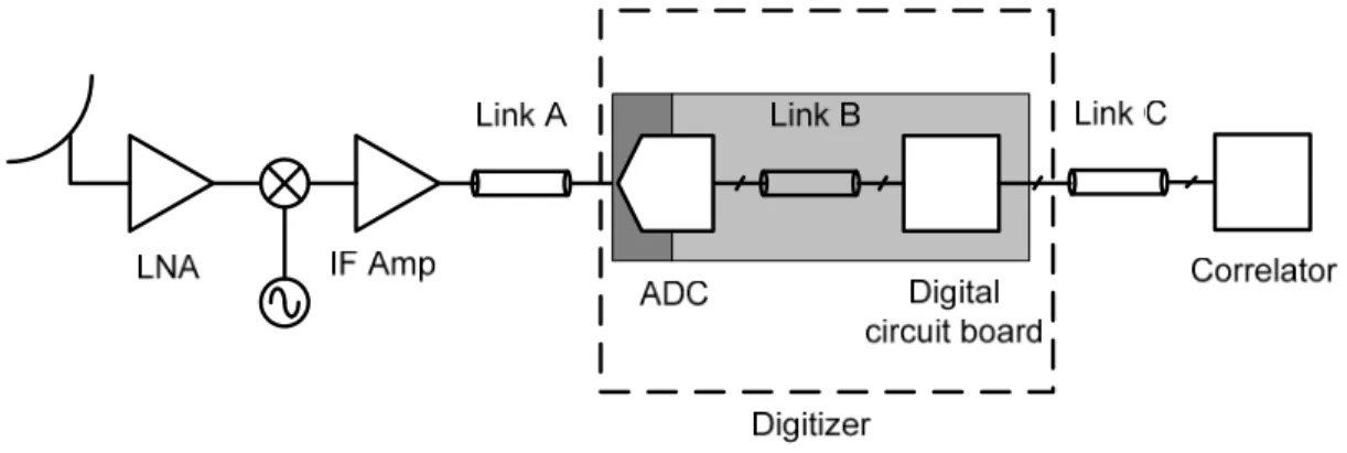
The transmission from receivers to digitizers or from digitizers to correlators is either via fiber in a long range distance or copper wires in a short range distance. In Figure 1, link A connects a receiver to a digitizer. Link C connects the digitizer to a correlator. Due to radio frequency interference (RFI) from digital circuits, correlators and digitizers are installed away from receivers. Thus, the IF signals from receivers are transmitted to digitizers via fiber cables. The wideband IF signal can be distorted by the nonlinear response of fiber cables and it is a serious problem. Massive digital signal processing is required to compensate the distortion before the correlator. Physical temperature variation can also change the characteristics of fiber cables in the frequency and time domains. The amplitude responses of optical to electrical (O/E) converters are nonlinear either. The dynamic range is severely compromised. To minimize these nonlinear effects, the digitizer location should be close to receivers once the RFI issue can be resolved.
*jshiao@phys.ntu.edu.tw, the Leung Center for Cosmology and Particle Astrophysics; phone +886 2-3366-8628
Millimeter, Submillimeter, and Far-Infrared Detectors and Instrumentation for Astronomy VI, edited by Wayne S. Holland, Jonas Zmuidzinas, Proc. of SPIE Vol. 8452, 84522K © 2012 SPIE · CCC code: 0277-786X/12/$18 · doi: 10.1117/12.924627
Proc. of SPIE Vol. 8452 84522K-1 Downloaded From: http://proceedings.spiedigitallibrary.org/ on 02/16/2013 Terms of Use: http://spiedl.org/terms
VDc IE YW r!UK 9 rvv r!UK I
Cooled semiconductor devices have been shown better performance [4,5]. The cooled device characteristics, including silicon–germanium heterojunction bipolar transistors (SiGe HBT) and complementary-symmetry metal–oxide– semiconductor (CMOS) transistors, have been measured at low temperature, 10-77 K. The measurement shows promising results for high speed circuit design. As CMOS ADCs consume less power than ever, cryogenic ADCs may become possible for coherent receivers. However, currently published reports about cryogenic CMOS ADCs are too few to draw a conclusion. Especially, ultra-deep submicron CMOS transistors (<100 nm) to date have been used in high speed and high density electronic devices. Their newly improved speed performance is comparable with SiGe HBTs. Moreover, CMOS processes have high integration feature, including calibration and digital signal processing. Thus, we have started to investigate the feasibility and performance of cryogenic high speed CMOS ADCs.
In this project, we first introduce the radio frequency interference problem of high speed ADCs and spread spectrum technology to lower the interference. Then we propose our ADC design using spread spectrum data clocks. Next we will show our ADC design using the spread spectrum technology. In Section 5, we present 4 bit 10 Gsps 65 nm CMOS ADC simulation results and test equipments. Finally, we conclude our current progress and summarize the future work.
Figure 1. The simplified system blocks from a receiver to a correlator. The light gray area is digital signal circuit in a digitizer; the dark gray area is analog signal circuit. The ADC consists of digital and analog signal circuits.
2. RADIO FREQUENCY INTERFERENCE AND SPREAD SPECTRUM TECHNOLOGY
Radio frequency interference (RFI), also known as electromagnetic interference (EMI), is a common issue in electronics systems. In a mixed-signal system like digitizers, strong digital signals usually disturb weak analog or RF signals via air, printed circuit boards (PCB), connectors or cables. The amplitude of high speed digital signaling levels, such as LVDS (Low-voltage differential signaling), is 0.4 V. The amplitude of a 0 dBm RF signal in a 50 Ohm system is 0.33V. When digital signals constantly change levels between high and low, sensitive receivers can easily pick up the high order harmonics leakage of the digital signals.
2.1 Location of digitizers
The easiest solution for RFI is to separate analog circuit and digital circuit in a system. The digital circuit boards can be put as far away from receivers as possible. However, as seen in Figure 1, an ADC consists of analog circuit and digital circuit in a single chip. If ADCs, as other digital circuits, are put away from receivers, it may not be easy to handle the nonlinearity of the optical link A. If ADCs are installed near receivers, their digital output signals, link B, can cause RFI to receivers. As a result, scientists have to carefully choose the location of digitizers in an array site.
2.2 Shielding
Grounding conductive enclosures can lower the RFI. To minimize the RFI, multi-layered shielding structure is perfectly sealed with absorbers to block the harmonics leakage. The RF and digital connectors are also need to be carefully chosen or designed. As a result, the shielding enclosure will be bulky and increases the digitizer design difficulty.
Proc. of SPIE Vol. 8452 84522K-2 Downloaded From: http://proceedings.spiedigitallibrary.org/ on 02/16/2013 Terms of Use: http://spiedl.org/terms
2.3 Spread Spectrum technology
Spread spectrum technology has been widely used in consumer electronics markets. Governments have established RFI regulations for various electronic devices at certain frequency bands. By changing strong signal tone frequency over a wide frequency range, the RFI can be lowered (see Figure 2). The strongest signal tone in digitizers is the sampling clock signal. The data streams are synchronized with the clock signal. While spread spectrum technology can be implemented in several ways, varying the sampling clock seems the most suitable for digital circuits. However, the coherence of the sampling clocks between digitizers and receivers has to be intact. Therefore, varying the output data clocks from ADCs is a better solution for coherent receivers. Many field-programmable gate array (FPGA) chips contain high speed SerDes transceivers up to 11.2 Gbps. The transceiver includes clock and data recovery (CDR) circuit to regenerate clock signal. Thus, spread spectrum digital data can be processed with FPGA chips.
Figure 2. Spectrum of a single tone signal without (see line A) and with (see line B) spread spectrum modulation. The spectral line of the signal will become continuum in the background.
3. CRYOGENIC ULTRA-DEEP SUBMICRON CMOS CIRCUITRY
Low cost SiGe HBTs have been used in cryogenic amplifiers [4]. The result shows that cryogenic SiGe transistors are suitable for low noise application. Cryogenic CMOS transistors also have been tested [5]. The result shows that ultra-deep submicron CMOS devices increase the speed performance at low temperature.
3.1 Cryogenic CMOS transistors
Ultra-deep submicron CMOS processes provide standard, high and low Vt MOS transistors for circuit design. Wind et al.
[5] report that low Vt MOS transistors are improved by low temperature for speed and current leakage. The carrier
mobilities are higher and the subthreshold characteristic slopes are steeper. Cryogenic CMOS circuits are suggested possibly work better than room temperature circuits by a factor of two. However, using submicron CMOS technology, Creten at al. [6] report that the performance of their ADC is degraded by low temperature, due to irregularity of MOS transistor characteristics at low temperature, such as I-V kinks and negative transconductance. The result shows that cryogenic CMOS circuit design may be a challenge.
3.2 Device models for circuit design
Device models are important to simulate circuit with computers and approximately predict measurement result. However, cryogenic device models are not supported by semiconductor manufactures. We suggest to design ADC circuits with more digital on-off functions and less linear circuits. Comparators and switches are more digital-like. Operational amplifiers, charge redistribution and current mirrors are linear circuits.
3.3 Power consumption and integration
The most important feature of ultra-deep submicron CMOS processes is low power consumption and high integration. Verbruggen et al. [7] present a 6 bit 2.2 Gsps ADC with only 2.6 mW. Using dynamic circuit technique, they manage to use minimum power to design a high speed ADC. This technique is only feasible in CMOS technology. Huang et al. design a 6 bit 16 Gsps ADC with digital background calibration technique. The integrated calibration circuit significantly improves the linearity of nonlinear ultra-deep submicron CMOS transistor characteristics. The calibration circuit is mostly digital and the power consumption is low. Therefore, despite of the uncertainties about cryogenic CMOS processes for transistors, the flexibility of high integration may overcome the uncertainties and reform cryogenic CMOS ADCs.
Proc. of SPIE Vol. 8452 84522K-3 Downloaded From: http://proceedings.spiedigitallibrary.org/ on 02/16/2013 Terms of Use: http://spiedl.org/terms
bps2e d IE 2!aUSI
4. PROPOSED CMOS ANALOG-TO-DIGITAL CONVERTERS
To design a cryogenic high speed CMOS ADC for coherent receivers, we carefully consider low temperature effect and large process variation. Exploiting the high integration feature of CMOS circuits, we may design auxiliary circuits to avoid the weakness of CMOS transistors and retain the low power and high speed features.
4.1 Ultra-deep submicron CMOS process
The most important issue for ultra-deep submicron CMOS processes is device mismatch. The threshold voltage, channel length and width, gate oxide thickness of a MOS transistor are random variables with sigma of more than 2%. This causes that the input offset voltages of comparators and amplifiers are not very uniform. For many ADC designs, the differentiation reflects the nonlinearity of ADC conversion; the digitized data is distorted. Second, compared with other high speed transistors, like SiGe HBTs, ultra-deep submicron MOS transistors have lower output resistance, ro, which
plays a critical role in transistor gain. The low gain decreases linear circuit performance in ADCs. Moreover, the operational supply voltage for these high speed transistors, VDD, is 1-1.1V. The input range of ADCs can not be larger
than VDD. Therefore, ADC input signal is more vulnerable to noise because of its small amplitude. 4.2 ADC system blocks
High speed ADC structures usually include pipelined, successive approximation (SAR), flash, folding and interpolation ADC types. To further increase the speed, time-interleaving technique is also commonly used to combine several ADCs as sub-ADCs, with properly different delayed sampling clocks. Combining n ADCs will give n times sampling rate at the output data. However, the input bandwidth of sub-ADCs needs to cover the frequency range.
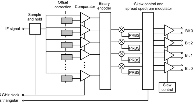
To lower the impacts of temperature and device mismatch uncertainties, we choose flash ADC structure as our 4-bit ADC design. We also use time-interleaving technique to combine four sub-ADCs to increase the sampling rate. Figure 3 is the ADC system blocks. The ADC is designed with 10 or 20 GHz sampling rate. Each sub-ADC conversion speed is 2.5 or 5 GHz. The sampling rate depends on many factors, such as the input bandwidth of the sub-ADC and the timing accuracy of multi-phase clock generator. The sub-ADC system blocks are shown in Figure 4. It consists of a sample and hold, comparators, offset correction, a binary encoder, PRBS modulators, skew control, spread spectrum modulator, output buffers and slew control. The reference voltages for comparators are generated by offset correction circuits with a resistor string.
Figure 3. Time-interleaving ADC system blocks. The ADC consists of a quad-phase clock generator and four sub-ADCs, which are flash ADCs. The IF signal is sampled by the sub-ADCs according to the precise timing controlled by the generator.
Proc. of SPIE Vol. 8452 84522K-4 Downloaded From: http://proceedings.spiedigitallibrary.org/ on 02/16/2013 Terms of Use: http://spiedl.org/terms
Comparator Bit 0 Bit 1 Bit 2 Bit 3 Binary
encoder spread spectrum modulatorSkew control and
PRBS PRBS PRBS PRBS Offset correction Sample and hold Slew control IF signal 5 GHz clock 10 kHz triangular wave
Figure 4. Sub-ADC system blocks include a sample and hold, comparators, offset correction, a binary encoder, PRBS modulators, skew control, spread spectrum modulator, output buffers and slew control.
4.3 Quad-phase clock generator
A time-interleaving ADC requires a multiphase clock generator to individually provide clocks for sub-ADCs. The variation between the sub-ADC clocks can cause distortion of output digital signals. So the delays of the clocks are critical. In our 65 nm and 45 nm CMOS ADCs, the number of sub-ADC is four, and thus, we design a quad-phase clock generator. Figure 5 shows the blocks of the clock generator, which includes, a phase-frequency detector, a charge pump, a loop filter/integrator and a voltage-control delay line (VCDL). The generator is basically a delay lock loop. The input signal is 5 GHz clock and the output quad-phase clocks will be locked at the same phase. So the total delay time of the VCDL is a period, 0.2 ns. VCDL contains four stages that generate four phase clocks. The phase detector compares the phase between the original 5 GHz clock and VCDL output clock, and then decides the charge pump to charge or discharge the loop integrator, a capacitor. The VCDL varies the delay between the stages accordingly until the loop feedback lock condition is satisfied.
Phase det. 5 GHz clock VCDL Charge pump Φ0 Φ1 Φ2 Φ3
Figure 5. Quad-phase clock generator. The input signal is 5 GHz clock. The delay lock loop will lock the VCDL with one period delay time from the input. The number of the delay stages in VCDL is four so the stages generate four phase clock signals.
Proc. of SPIE Vol. 8452 84522K-5 Downloaded From: http://proceedings.spiedigitallibrary.org/ on 02/16/2013 Terms of Use: http://spiedl.org/terms
4.4 Comparator and input offset mismatch correction
As mentioned above, 45 and 65 nm comparators seriously suffer from the input offset voltage mismatch issue. We suggest using offset correction circuit to calibrate each comparator. While one sub-ADC consists of only 15 comparators, the individual correction is still doable. Once the ADC is power on and reset properly, the ADC self-generates a triangular wave as the input test signal to test each comparator. The offset voltage will be measured and stored in registers in the ADC. After the self-calibration process is completed, the ADC sends a RDY signal and waits for converting actual signals. The calibration can also continue statistically in the background with more than one round when the non-conversion time is sufficient.
4.5 ROM Encoders
We design the binary encoder with the popular ROM (Read-Only Memory) architecture, which is one of the fastest circuit topology. With high speed and high gain transistors, like SiGe BJT devices, the Gray encoder with folding architecture is more adequate and consumes less power. However, ultra-deep submicron CMOS transistors are high speed but low gain. The binary encoder is better.
4.6 PRBS random generator
The ADC core supply voltage is 1-1.1V, which is below than LVDS high levels. The output data signals have to be capacitively coupled to FPGA LVDS transceivers. PRBS random generators are used to modulate the data signal to higher frequency so the capacitive coupling can transmit low frequency data as well as high frequency data to transceivers. The CDR (Clock Data Recovery) circuit in FPGA transceivers can reproduce synchronized clock to reconstruct the data. The PRBS polynomial is X7+X6+1.
4.7 Spread spectrum clock and skew control
The output clocking scheme uses spread spectrum technology to lower RFI in the frequency domain. Moreover, skew control is also used to avoid ringing on supply voltage and then further causing glitches to the other circuits in the ADC. The 5 GHz clock signal is phase modulated with a lower frequency signal by changing the delay of another VCDL. The modulation signal is usually a triangular wave. The spectrum spread clock is then sent to the output buffers. The time window of the data signals that allow the clock to sample or latch is very narrow and may be varied by processes. The maximum extra delay should less than a half clock period, 0.1 ns. However, the initial clock edge position may already be early or late for the perfect position. Thus modulation signal is controlled flexibly from the outside of the ADC. The skew control is also important for ultra-deep submicron CMOS ADCs because of their vulnerability to voltage power supply and subtract noise pickup. In Figure 6, using skew controlling, the output buffer clocks are spread at different time, which minimize the impact of the output buffer currents on power and subtract voltages. The output data channels have individual clock skews to prevent all buffers switch levels at the same time, which will lower the noise on supply voltage.
4.8 Slew controlled LVDS output buffers
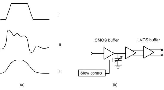
Finally, the digitized data is transmitted from ADCs to FPGA by LVDS buffers. To further lower the RFI, the rising and falling time of the output waveform are controlled digitally. The rising and falling time is aspect of slew rate. The output buffer are connected with bonding wires to packages and then to PCBs. The lump circuit model of the wires and package legs are inductive. The inductance and parasitic capacitance combined become a resonant circuit and cause overshoot and undershoot effects on output signals (Figure 7(a)). The overshoot and undershoot signals contain high harmonics noise that can be transmitted via the wires and legs. To optimize the output signals without ringing supply voltages and signals, we use a series of capacitors to change the signal slew rate that drive the output buffers in Figure 7(b). The CMOS buffer is considered as current source. The controlled capacitors change the charge speed for the current source.
Proc. of SPIE Vol. 8452 84522K-6 Downloaded From: http://proceedings.spiedigitallibrary.org/ on 02/16/2013 Terms of Use: http://spiedl.org/terms
ACD[
DGI9A CG
Figure 6. Spread spectrum modulation and skew control blocks. We use a triangular wave to modulate the delay of data clock. There are four different delay cells individually for the four output channels.
Figure 7. (a) Waveform I is the ideal case. Waveform II contains overshoot and undershoot that enhance high order harmonics. Waveform III is slew controlled waveform. (b) Slew control circuit. The slew rated is digital controlled by a varactor that consists of
parallel capacitors.
5. SIMULATION RESULTS AND TEST SETUP
While the 40 nm CMOS ADC circuit design is still on-going, we show the 65 nm CMOS ADC simulation results. The 65 nm CMOS ADC has been taped out to manufacture.
5.1 Comparator
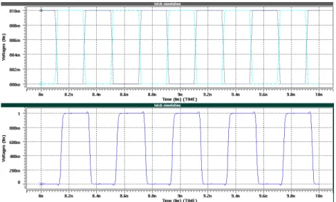
Monte Carlo simulation shows that the sigma of 65 nm CMOS comparator offset is 40 mV. The 4 bit ADC input voltage range is 0.5-1 V so the LSB is 31 mV. The offset correction should reduce the offset down to 10 mV. The speed of comparators can be tested with a small signal. Figure 8 shows the input of output of a comparator at 5 GHz. The 2.5 GHz input differential signals are 10 mV and the output signal is CMOS level.
Proc. of SPIE Vol. 8452 84522K-7 Downloaded From: http://proceedings.spiedigitallibrary.org/ on 02/16/2013 Terms of Use: http://spiedl.org/terms
Figure 8. The top shows the input differential signals. The bottom shows the comparator output signal.
5.2 Quad-phase clock generator
The VCDL in the quad-phase clock generator can be simulated by varying the input control voltage. By sweeping the voltage, we obtain the changed delays of the four phase clock signals in Figure 9.
Figure 9. The first, second, third and fourth waveforms are the four output clock signals. The varied delay clocks are overlaid together to show the delay differentiation by the control voltage from 0.4 to 1 V with a 0.1 V step.
5.3 ENOB
The effective number of bits (ENOB) is estimated with signal-to-noise and distortion ratio (SNDR). When input frequency is 5 GHz and the sampling rate is 10 GHz, the ENOB is about 2.4. The input frequency can be improved up to 10 GHz by an input match network, which will be included in the future. The power consumption is 20 mW.
Proc. of SPIE Vol. 8452 84522K-8 Downloaded From: http://proceedings.spiedigitallibrary.org/ on 02/16/2013 Terms of Use: http://spiedl.org/terms
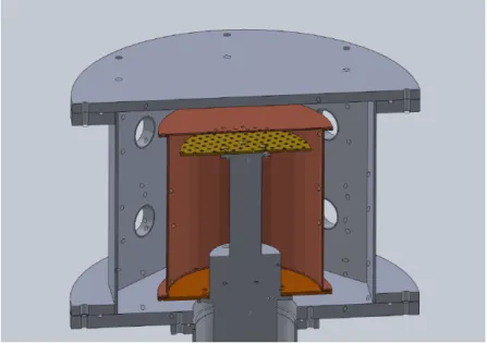
5.4 Dewar Setup
The 10 K dewar has a single layer shield at 70 K, as shown in Figure 10. There are four RF and four DC feedthoughs on the sides. The first stage of the cryocooler is only used as a thermal radiative shield. The second stage is a copper platform for mounting ADCs and other electronic devices.
Figure 10. Dewar for cryogenic CMOS ADC testing.
6. CONCLUSIONS
A cryogenic analog-to-digital converter design has been proposed and it may significantly increase coherent receiver performance by spread spectrum technology and low temperature. Cryogenic semiconductor CMOS or SiGe HBT devices are improved in many ways, gains, carrier mobilities. The device thermal noises are lower as well. Lack of transistor models may be overcome by circuit system design accordingly. To lower the EMI from ADCs in or near receivers, we suggest using spread spectrum technology for the output data streams. Thus, the clock alignment between a single coherent receiver and the others remains intact. The clock data recovery can be processed by high speed FPGA’s 11.2 Gpbs receivers.
Our cryogenic EMI test system is still on-going and we design two CMOS ADCs to investigate the effect in our design. To design a high speed ADC, a multi-phase clock generator will be integrated to provide proper timing clocks for sub-ADCs. To use spread spectrum technology, a modulator constantly changes the delay of a VCDL that controls the output data clock and minimizes the sampling clock power leakage and its harmonics. The modulator signal can be either externally from a signal generator or internally self-generated. The ADC also includes PRBS pseudo random number generators as noise sources to dither the output data stream so the capacitive coupling can be used to avoid the low supply voltage of the ADC.
The sub-ADC structure is chosen conservatively to be flash ADC type. A flash ADC consists of comparators, a binary encoder and output buffers. As its simplicity, the power consumption is high and so is the input offsets of the comparators. We use ultra-deep submicron CMOS processes to lower the power consumption and massive offset correction circuits to compensate the offsets. The newly simulation shows the 4 bit 10 Gsps 65 nm CMOS ADC only needs 20 mW, including the output buffers. The future 40 nm CMOS ADC should work even better. Thus, the ultra low power consumption is the biggest advantage of cryogenic CMOS ADCs.
Proc. of SPIE Vol. 8452 84522K-9 Downloaded From: http://proceedings.spiedigitallibrary.org/ on 02/16/2013 Terms of Use: http://spiedl.org/terms
ACKNOWLEDGEMENTS
We thank National Nano Device Laboratories for ADC testing and Taiwan Semiconductor Manufacturing Company Limited (TSMC) for chip manufacture. This project is partly supported by the National Science Council under the grant NSC100-2112-M-492-001-MY3.
REFERENCES
[1] Baryshev, A.M., Hesper, R., Mena, F.P., Jackson, B.D., Adema, J., Barkhof, J., Wild, W., Candotti, M. Whale, M., Lodewijk, C. Loudkov, D., Zijlstra, T. and Klapwijk, "Performance of ALMA band 9 receiver series," 18th Int. Sym. on Space Terahertz Tech., 164-167 (2007).
[2] Wright, M. , "Allen Telescope Array Imaging," ATA memo 52, (2002).
[3] Hawkins, D. W., Woody, D. P., Wiitala, B. and Fredsti, J., "The CARMA correlator," Proc. SPIE 5498, 567-569 (2004).
[4] Weinreb, S., Bardin, J.C. and Mani, H., "Design of Cryogenic SiGe Low-Noise Amplifiers," IEEE Tran. On Microwave Theory and Tech., 55, 11, 2306-2312 (2007).
[5] Wind, S.J., Shi, L., Lee, K.-L., Roy, R.A., Zhang, Y., Sikorski, E., Kozlowski, P., D'emic, C., Bucchignano, J.J., Wann, H.-J., Viswanathan, R.G., Cai, J. and Taur, Y., "Very high performance 50 nm CMOS at low temperature," Int. IEDM Tech. Digest., 928-930 (1999).
[6] Okcan, B., Merken, P., Gielen, G. and Van Hoof, C. , "A cryogenic analog to digital converter operating from 300 K down to 4.4 K," Rev. of Sci. Ins., 81, 2, 024702 (2010).
[7] Verbruggen, B., Craninckx, J., Kuijk, M., Wambacq, P. and Van der Plas, G., "A 2.6 mW 6 bit 2.2 GS/s Fully Dynamic Pipeline ADC in 40 nm Digital CMOS," IEEE JSSC, 45, 10, 2080-2090 (2010).
[8] Creten, Y., Merken, P., Sansen, W., Mertens, R. and Van Hoof, C., "A Cryogenic ADC operating Down to 4.2 K," IEEE ISSCC Digest of Tech. Papers, 468-616, 11-15 (2007).
[9] Huang, C.-C., Wang, C.-Y. and Wu, J.-T., "A CMOS 6-Bit 16-GS/s Time-Interleaved ADC Using Digital Background Calibration Techniques," IEEE JSSC, 46, 4, 848-858 (2011).
Proc. of SPIE Vol. 8452 84522K-10 Downloaded From: http://proceedings.spiedigitallibrary.org/ on 02/16/2013 Terms of Use: http://spiedl.org/terms