A 90 nm All-digital Smart Temperature Sensor with Wireless
Body Area Network Baseband Transceiver
for Biotelemetry Applications
Ching-Che Chung&Jui-Yuan Yu&Shiou-Ru Jang& Chen-Yi Lee# 2010 Springer Science+Business Media, LLC. Manufactured in The United States
Abstract This work provides an all-digital smart temper-ature sensor with dual-mode transceiver chipset for wireless body area network (WBAN). The measurement results show that the proposed temperature sensor achieves a maximum temperature error<0.6ºC within the range from 20ºC to 50ºC. And a phase-frequency tunable clock generator (PFTCG) is designed with frequency and phase tuning capability on the fly. This chip is manufactured on a standard 90 nm CMOS process. The supply voltage to the chip core is globally applied at 0.5 V with 12 power-domain partitions for sleep-active and voltage-scaling management. The transceiver chipset provides maximum 7 Mbps data rate, resulting in 97.7% efficiency improve-ment in baseband circuit processing.
Keywords PLL . Temperature sensor . Power domain . Voltage scaling . WBAN
1 Introduction
Ubiquitous healthcare monitoring plays a crucial role in physical status tracking and recording. This extends medical services from the closed in-hospital systems to any open roaming spaces. Wireless body area network
(WBAN), consisting of a multiple wireless sensor nodes (WSNs) and a central processing node (CPN) [1], is specifically designed for bio-signal acquisition and moni-toring to provide reliable physical information. The WSN is capable of sensing and processing body information, and transmitting the data wirelessly to a CPN. The WBAN, especially the WSN, is required to provide reliable signal exchanges with ultra-low power and highly integrated tiny chip area.
WBAN-oriented applications may cover from non-invasive to implanted systems that further differ in data rate requirements. Moreover, the wireless channel condi-tions inside a body also perform different features from that on the skin surface. Existing possible systems [2,3] for the WBAN applications, however, provide single modulation scheme that have difficulty meeting the whole application spectrum with unacceptable power consumption. Further-more, those candidate systems operate at the industry-science-medical (ISM) band may easily be fully occupied by unexpected interference. Accordingly, Federal Commu-nications Committee (FCC) defines a set of wireless medical telemetry service (WMTS) band [4], and our previous proposal [1] was designed under the basis of the WMTS constraints.
It is necessary to provide a dedicated hardware solution for microwatt WBAN applications. State-of-the-art plat-forms [5, 6] achieve highly integrated SoC designs with mature FSK wireless scheme. An alternative RF front-end design [7] focuses on a pulse-based radio transmission. Those designs are implemented with above 1 V supply voltage and milli-order power consumption.
The proposed WBAN platform contains a WSN and a CPN that are attached on human body skin and integrated in a portable device, respectively. The system block diagram is illustrated in Fig. 1. A FIFO-based memory is
C.-C. Chung (*)
Department of Computer Science and Information Engineering, National Chung Cheng University,
Chia-Yi, Taiwan
e-mail: [email protected] J.-Y. Yu
:
S.-R. Jang:
C.-Y. Lee Department of Electronics Engineering, National Chiao Tung University, Hsinchu, TaiwanDOI 10.1007/s11265-009-0448-y
designed in the WSN that is used to record body signals from internally integrated all-digital smart temperature sensor or other external connected body sensors. The memory size and clocking speed are optimized for and aimed at the electrocardiography signal that are regarded as the most complex signals among body information sources. Compared to the baseband processing speed, the WSN takes much longer time to record body signals. This results in the WSN-CPN pair staying inactive for most of time and awake in burst for data transmission. The clock sources in the WSN and CPN are implemented by a phase-frequency tunable clock generator (PFTCG). It is used to adjust the generated clock phase and frequency automatically for better system performance and reduced power consumption. Each block in both the WSN and CPN is designed for a specific power-voltage domain for low-power management.
2 System Overview
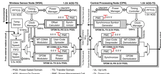
The WBAN transceiver chipset is designed with power-domain partitions for voltage scaling, multi-supply voltage (MSV), and power gating to achieve extreme low power consumption as illustrated in Fig. 2. With the voltage scaling and multi-supply voltage techniques, the system is partitioned into 12 power domains with possible different voltage supplies.
According to the required operating speed and the achievable functionality, the supply voltage 0.5 V is provided globally to every functional block, except special function blocks and transfer-domain (TD) that are operated at 1.0 V to interface with I/O pads. Furthermore, every power domain is not necessary to be activated together. So, the other inactive domains can be switched into sleep phase for most leakage power saving. This active-sleep behavior is achieved by a power management cell (PMC) that contains distributed coarse-grain power gating cells (DCG-PGC) [1] and isolation cells.
The power manager sends commands to the PMC to turn ON/OFF the power-gated domain (PGD). When an OFF signal is asserted, the isolation cell first de-activates by pulling high the signal in the always-on-domain (AOD) side. After that, the DCG-PGC shuts the virtual VDD off. Therefore, the unknown signal from the power-off domain will not affect the other domains. The PMC behavior is in the reverse way when a domain goes to active state. On the other hand, if a hardware block always stays active, its power will not be gated and is referred as always-on domain (AOD).
In addition, the chipset has several clock domains to drive different sequential circuits. For the MT-CDMA block, a clock of 1/31 time of the original frequency is needed. Besides, a low frequency clock to record the body sensor’s output is necessary. Therefore, an embedded clock
FIFO OFDM UL-TX MT-CDMA TX PFTCG 5 MHz PFTCG 5 MHz OFDM UL-RX MT-CDMA RX OFDM DL-TX Temp. Sensor OFDM DL-RX
Wireless Sensor Node (WSN)
Variable power domain partitions
Central Processing Node (CPN)
Portable Device
Figure 1 The functional blocks of WSN and CPN baseband transceiver. Temp. Sensor PFTCG FIFO 1.0V AOD 0.5 V Clock Manager Wireless Sensor Node (WSN)
- PGD: Power-Gated Domain OFDM DL-RX (0.5v PGD) 0.5v AOD 1.0V AOD-TD Synch-ronizer Offset Calculator 0.5 V OFDM UL-TX (0.5v PGD) Phase Rotator OFDM Modulator MT-CDMA (0.5v PGD) User-Code Spreader MT-CDMA Modulator 0.5 V
From external rea
d o ut c ircuit To the front -e nd Fr om t h e fr ont end Timing Controller PMC PMC PMC Power Manager 5MHz 5MHz 161K H z 610Hz PMC 1.0V AOD-TD Central Processing Node (CPN)
OFDM UL-RX (0.5V PGD) Synchronizer OFDM Demodulator 0.5 V PMC F ro m th e front en d T o t he fron t-e n d OFDM DL-TX (0.5V PGD) Synchronous Symbol Generator 0.5 V PMC Timing Controller Power Manager Clock Manager MT-CDMA (0.5V PGD) User-Code Despreader MT-CDMA Demodulator 0.5 V PMC 161K H z 5MHz PFTCG 1.0V AOD B it s tr e a m ou tp ut ON/OFF ON/OFF PMC Low-Speed High-Speed Da ta C o nv e rt e rs / RFs/ Wireless Ch an n e l En v ir o nm en tal temperature
- PMC: Power Management Cell - AOD: Always-On Domain
- TD: Transfer Domain - UL: Up-Link - DL: Down-Link
Figure 2 The detail baseband transceiver block diagram (WSN and CPN).
generator provides the 5 MHz clock source, and a clock manager unit is designed for frequency synthesis. The synthesized frequency outputs 5 MHz, 161 kHz, and 610 Hz clocks to cover all possible requirements.
There are total three operation modes in the WSN, MT-CDMA TX, OFDM DL-RX, and OFDM UL-TX, to support the dual mode transmission and pre-calibration. First, in the MT-CDMA TX mode, FIFO stores the sensed signals whereas the MT-CDMA transmitter is idled in the sleep phase. When the stored data in low-speed FIFO is full, the MT-CDMA transmitter is waked up to transmit those signals in the active phase. The 161 kHz and 5 MHz clocks are used for modulation and user code spreading respectively.
Second, in the OFDM DL-RX mode, the OFDM receiver is synchronized to the downlink training symbols and calculates the frequency offset for pre-calibration. The 5 MHz clock is used for the OFDM receiver block as well as the OFDM transmitter block.
Lastly, when WSN operates in the OFDM UL-TX mode, the OFDM transmitter can also be separated into two phases. OFDM transmitter is in active phase when transmitting the data and in sleep phase when waiting for the sensed data storing. The frequency offset is pre-calibrated by the digital data distortion and tuning the frequency generated from PFTCG. In these modes, only the corresponding PGD is waked up, the other PGDs are turned off to save the leakage power.
An all-digital smart temperature sensor is integrated in the WSN. The measured temperature data and other
external sensor data are stored in the register-based FIFO. The biomedical signal is highly correlated in time domain so that a FIFO has benefits in the minimum switching power consumption, resulting in both reduced dynamic and leakage power for body-oriented signal storage.
The total size of FIFO is 1024x8 bits that are further equally divided into two banks. One of the FIFO banks is driven by the 610 Hz clock, which is synchronous to the sensor data. The other bank operates at 5 MHz and delivers the data to the baseband modulator. The low speed bank collects data in longer period until it is full. As the content of the low speed bank is full, the bank dumps all its content to the high speed bank and can continue on collecting the data without any loss.
PFD Controller DCO M U X PH7 PH1 PH0 UP DOWN LOCK REFCLK DCO_CODE FE OUT_CLK Phase_Selection PE In
Figure 3 The proposed PFTCG architecture.
Figure 4 The BJT-based smart temperature sensor.
20 25 30 35 40 45 50 1970 1980 1990 2000 2010 2020 2030 24SL400 (interval=1) pu range=47.0000ns R-square=0.38643 temperature pu (ns) pu
Figure 5 The pulse width of the temperature sensor implemented with 90 nm short-channel MOS devices.
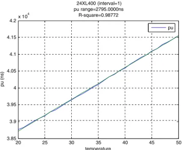
20 25 30 35 40 45 50 3.85 3.9 3.95 4 4.05 4.1 4.15 4.2x 10 4 24XL400 (interval=1) pu range=2795.0000ns R-square=0.98772 temperature pu (ns) pu
Figure 6 The pulse width of the temperature sensor implemented with 90 nm long-channel MOS devices.
The CPN has three operation modes, MT-CDMA RX, OFDM DL-TX, and OFDM UL-RX, in CPN. First, when CPN operates in the MT-CDMA RX mode, the received data from the front-end is directed to the MT-CDMA receiver block. The data is first de-spread by the 31-chip user code followed by the MT-CDMA demodulator. The synchronizer of MT-CDMA is able to calculate a better sampling phase for the PFTCG. Second, in OFDM DL-TX mode, the OFDM DL-TX broadcasts synchronous symbols and the content of the synchronous symbols is adjustable depending on the user selection. Lastly, in the OFDM UL-RX mode, the received data is switched to the OFDM uplink receiver where the synchronization block is first encountered followed by the OFDM demodulation block.
When CPN is in one of the operation modes, the corresponding PGD is activated and the others are in sleep phase. The rest block of CPN is PFTCG, which generates a 5 MHz clock with eight different phases for synchronization. This clock signal is sent to the clock manager unit, where a 5 MHz clock is bypassed to all the three blocks and a 161 kHz clock is generated for the MT-CDMA demodulator. The phase-frequency tunable clock generator (PFTCG), as shown in Fig.3, is designed for performance improve-ment in WSN and power reduction in CPN. There are four major blocks, including phase-frequency detector (PFD), controller, digitally-controlled oscillator (DCO) and phase selection multiplexer. The PFD generates UP or DOWN commands to modify the frequency of DCO in the tracking loop. When this loop achieves the lock state, the resulting
clock frequency corresponds to the desired 5 MHz clock, which is regarded as the coarse tuning step.
The DCO further generates eight multi-phases as the lock state is reached. It is designed with eight same delay cells, and each delay cell provides TREFCLK/8 delay time, resulting in eight equally-spaced multi-phase clock signals between Cycle_N and Cycle_(N+1). Then one of these 8 sources is selected via the phase-selection. The correct frequency is generated by the closed loop of PFD, controller, and the phase_0 (PH0) in the DCO. This guarantees the resulted clocks keep the same delay spacing TREFCLK/8 when the process-voltage-temperature (PVT) condition changes.
The PFTCG allows the WSN and CPN to slightly change the generated clock frequency and phase by sending a command frequency-error (FE) and phase-error (PE) to the controller and multiplexer, respectively. This frequency fine-tuning capability reduces the sampling clock offset between the WSN and CPN for better performance, and the phase-selection capability enables the CPN to sample incoming signals at better instances without increasing sampling frequency.
3 On-chip Temperature Sensor
The on-chip body temperature sensor for biotelemetry applications must be small area, low-power consumption and easy integration with the transceiver. The temperature sensor should have extreme low-power consumption to avoid self-heating effects to the system, and it must be easy to perform absolute temperature calibration and has sufficient conversion rate to dynamically monitor the body temperature profile.
Traditionally, temperature sensors are built by thermis-tors or platinum resisthermis-tors, and require separate readout circuitry. The smart temperature sensor combines sensor and interface electronics into a single chip, and it can be manufactured on the low-cost CMOS process. Hence it becomes more and more popular today.
Pulse Generator ENABLE
Time-to-Digital Converter
Proportional to Absolute Temperature (PTAT)
PU Digital Output
Figure 7 The proposed all-digital smart temperature sensor architecture.
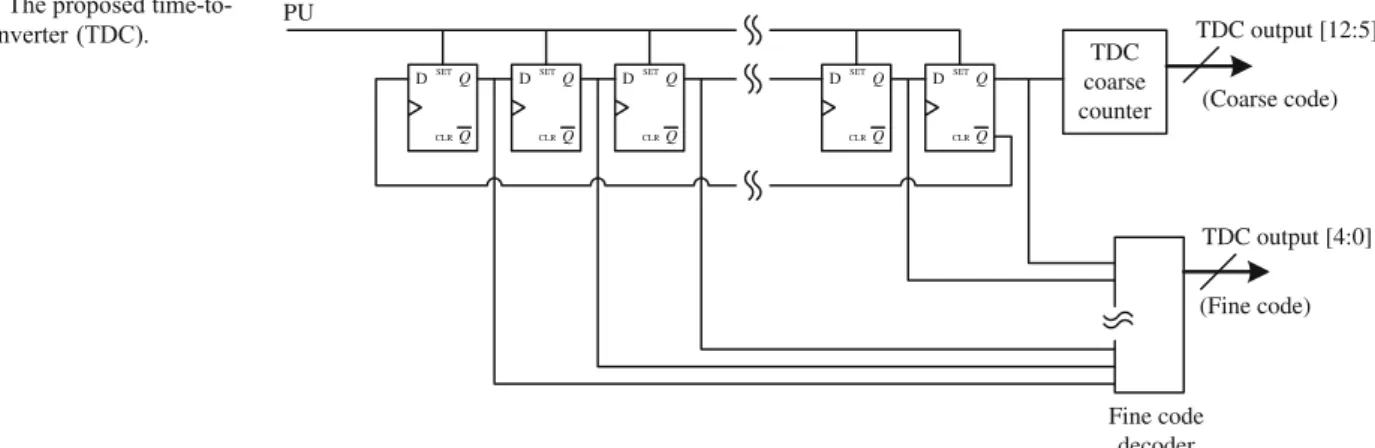
Q Q SET CLR D Q Q SET CLR D Q Q SET CLR D Q Q SET CLR D Q Q SET CLR D TDC coarse counter Fine code decoder TDC output [4:0] TDC output [12:5] (Fine code) (Coarse code) PU
Figure 8 The proposed time-to-digital converter (TDC).
The BJT-based smart temperature sensors are widely used in many applications. Figure4 shows the concept of BJT-based smart temperature sensors [8]. The temperature sensor generates a voltage (VPTAT) proportional to the absolute temperature. The reference block generates a constant voltage (VREF) which is independent of the temperature within the operation range. Then the analog-to-digital converter (ADC) converts the difference between VPTATand VREFinto a digital code (TS_OUT). However, it is not possible to keep the reference voltage (VREF) constant over the whole temperature range with process and voltage variations. As a result, second order curvature correction circuit, sigma-delta modulator, and post-silicon transistor trimming are used in the sensor [8] to improve the accuracy of temperature measurement. However these calibration circuits increase the circuit complexity and are not suitable for 90 nm process which often with 1.0 V low supply voltage. The total power consumption and chip area are also increased due to the bias circuits and the calibration circuits. And it also takes more efforts to integrate the analog circuits with the digital circuits. As a result, the BJT-based smart temperature sensors are not suitable for on-chip body temperature sensor in biotelemetry applications.
The propagation delay of the delay line can be used to measure the temperature. The delay line-based smart temperature sensor [9] first generates a pulse with a width proportional to the absolute temperature. Then, a cyclic time-to-digital (TDC) converter is utilized to convert this pulse into a corresponding digital code. The advantage of this architecture is that it is a fully digital circuit and is easy integrated with other digital circuits. However the proposed cyclic TDC [9] with pulse-shrinking mechanism takes a long time to convert the pulse width into the digital codes. Therefore the other delay line with low thermal sensitivity is needed to cancel the DC offset and reduce the TDC conversion time. As a result, chip area and power consumption are increased due to the two delay lines architecture.
Figure5 shows the simulation results of the delay line-based smart temperature sensor implemented with 90 nm short-channel MOS devices. However, the propagation delay is not linearly proportional to the absolute tempera-ture when short-channel MOS devices are used. But if the long-channel MOS devices are used in the delay line circuit, the linearity can be improved as shown in Fig.6. As a result, in the proposed smart temperature sensor, long-channel MOS devices are used to build up the delay cell of the delay line. And therefore the temperature error due to the nonlinearity of the propagation delay can be reduced.
Figure 7 shows the architecture of the proposed all-digital temperature sensor. To reduce chip area and enhance resolution of the digital read-out circuit, a cyclic delay line with a pulse generator is used to generate a long duration pulse. The cyclic delay line is a temperature-to-pulse generator. It is used to generate a pulse and its width is proportional to the absolute temperature (PTAT). The delay cells in the cyclic delay line are built with the long-channel MOS devices. The pulse generator counts the positive edge triggers from the cyclic delay line, and when a specified value N is reached in the counter, the cyclic delay line is stopped. Then the pulse width of the output signal “PU” becomes N×Td, where Td means the period of cyclic delay line’s output, and the time-to-digital converter (TDC) is utilized to quantize the pulse width of“PU” into the digital codes.
Table 1 Comparisons of recent smart temperature sensor.
Sensor Error(ºC) Power Area
(mm2) Conversion Rate (samples/sec) Temperature Range(ºC) CMOS Technology [8] ±0.1 (3σ) 247 μW@ 3.3 V 4.5 10 −55∼125 0.7 μm [9] −0.7∼+0.9 0.49 mW@ 3.3 V 0.175 1,000 0∼100 0.35 μm [10] −1.8∼+2.3 12 mW@ 1.2 V 0.16 5,000 0∼100 0.13 μm proposed ±0.6 0.38 mW@ 1.0 V 0.12 1,000 20∼50 90 nm
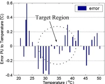
Figure 9 The measurement results of the proposed all-digital smart temperature sensor.
Figure 8 shows the architecture of the proposed TDC. The TDC is composed of the coarse counter and the fine code decoder to achieve high resolution quantization. In the proposed TDC, 16 latches are used to compose the TDC cell line. When the signal “PU” outputted from the pulse generator is enabled, then all latches in the TDC cell line are turned on and the TDC cell line starts to oscillate. The TDC’s coarse counter counts the arrival positive edges to generate the TDC coarse code. This operation is continued until the signal“PU” is disabled. Then the residual pulse width information can be generated after the fine code decoder. And the output of the TDC coarse counter and the fine code decoder are combined as the TDC_output[12:0]. The resolution of the TDC is limited by the propagation delay of the TDC cell line and the setup/hold time requirements of the latches. As a result, the TDC must perform simulation with PVT variations to make sure that the output temperature error are not mainly comes from the TDC. Then we can get the absolute temperature informa-tion after one-point or two-point temperature calibrainforma-tion during chip measurement.
4 Experimental Results
The proposed all-digital smart temperature sensor with WBAN baseband transceiver chipset is fabricated on a standard 90 nm 1P9M CMOS process. Figure 9shows the measured temperature error of the proposed temperature sensor. This temperature sensor is designed for human body temperature measurement in the range from 35ºC to 40ºC. The proposed design performs good linearity in this range and achieves error<0.6ºC.
Table1lists the comparisons of recent smart temperature sensors. In BJT-based smart temperature sensor [8], the sensor has large chip area because of the complex calibration circuits. And this sensor can only achieve a maximum conversion rate at 10 samples/sec. In the all-digital smart temperature sensors [9, 10], the proposed design can achieve higher conversion rate with lower power consumption. And the two-point temperature calibration is performed in the proposed design. Although the tempera-ture error is very small (±0.1ºC) in [8], this BJT-based temperature sensor is not suitable for on-chip body
Timing Synchronizer Post-FFT Sync. FFT Misc. Pre-FFT Sync. Timing Sync. FFT(1) FFT(2) Post-FFT Sync. Equalizer Data Decoder PFTCG OFDM-DLTX Timing Synchronizer SCO Est. CFO Est. Equalizer Packet Detector FFT MT-CDMA TX FIFO OFDM-UL modulator PFTCG Temp. Sensor PR OFDM-UL TX OFDM-DL RX OFDM-UL RX MT-CDMA Transfer Domain Transfer Domain
Figure 11 The microphotograph of WSN and CPN.
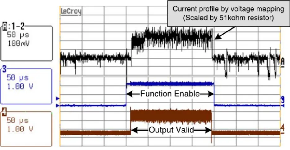
Function Enable
Output Valid
Current profile by voltage mapping (Scaled by 51kohm resistor)
Figure 10 The current profile between sleep and active modes.
temperature sensor in biotelemetry applications. And in [10], the high power consumption and large chip area makes it is also not suitable for biotelemetry applications.
The power-domain of this chip is turned on by the DCG-PGC. The OFDM DL-TX building block is used for the illustration of the current profile between active and sleep states. This current profile is generated by concatenating a resistor (51 k ohm) in the way of core power path for clear instrument observation, and the voltage between this resistor’s two sides is shown in Fig. 10. As the ENABLE signal is activated, the OFDM DL-TX domain is turned on, and more current is drawn that corresponds to μ-level power consumption.
This WBAN transceiver improves the system data rate from 143 kbps to 7 Mbps. This largely reduces the system working duty cycle (i.e. the percentage of circuit active time). The transmission energy is reduced from previous proposal 21 μW [1] to this work 5.52 μW, resulting in 73.7% efficiency improvement in baseband circuit processing. Figure11 shows the micro chip photos. Each bold-rectangular denotes a separate power domain with the rest region as the transfer domain for I/O-pad interfaces.
5 Conclusions
This work provides an all-digital smart temperature sensor with dual-mode baseband transceiver chipset for wireless body area network (WBAN). The proposed delay line-based all-digital smart temperature sensor implemented with long-channel MOS devices achieves good linearity in temperature measurement. A clock generator with frequen-cy and phase tuning capability is provided for system performance improvement and power reduction. The supply voltage is scaled to 0.5 V with dedicated power-domain partitions. The power efficiency is improved in baseband signal processing. As a result, this work provides an extreme low-power and highly-integrated WBAN platform, especially suitable for the biotelemetry applications.
Acknowledgement The authors would like to thank United Micro-electronics Corporation (UMC) for the university shuttle program in fabricating the test chip and Cadence Design Systems for EDA tool support.
References
1. Yu, J-Y., Chung, C-C., Liao, W-C., & Lee, C-Y. (2007). A sub-mW multi-tone CDMA baseband transceiver chipset for wireless body area network applications. ISSCC Dig. Tech. Papers, 364–365.
2. Wireless Medium Access Control (MAC) and Physical Layer (PHY) Specifications for Wireless Personal Area Networks (WPANs), IEEE Standard 802.15.1, 2005.
3. Wireless Medium Access Control (MAC) and Physical Layer (PHY) Specifications for Low-Rate Wireless Personal Area Networks (LR-WPANs), IEEE Standard 802.15.4, 2003. 4. Federal Communications Commission (2000). Amendment of parts
2 and 95 of the Commission’s rules to create a wireless medical telemetry services. FCC Washington, D.C., Rep. FCC00-211. 5. Wong, A. C-W., Mc Donagh, D., Kathiresan, G., Omeni, O. C.,
El-Jamaly, O., Chan, T. C-K., et al. (2008). A 1 V, micropower system-on-chip for vital-sign monitoring in wireless body sensor networks. ISSCC Dig. Tech Papers, 138–139.
6. Wong, A. C. W., Kathiresan, G., Chan, C. K. T., Eljamaly, O., & Burdett, A. J. (2007). A 1 V wireless transceiver for an ultra low power SoC for biotelemetry applications. ESSCIRC Dig. Tech. Papers, 127–130.
7. Guermandi, D., Gambini, S., & Rabaey, J. (2007). A 1 V 250 Kbps 90 nm CMOS pulse based transceiver for CM-range wireless communication. ESSCIRC Dig. Tech. Papers, 135–138. 8. Pertijs, M. A. P., & Huijsing, J. H. (2005). A CMOS smart
temperature sensor with a 3 sigma inaccuracy of +/− 0.1 degree from −55 degree to 125 degree. IEEE Journal of Solid-State Circuits, 40, 2805–2815.
9. Chen, P., Chen, C.-C., Tsai, C.-C., & Wen-Fu, Lu. (2005). A time-to-digital-converter-based CMOS smart temperature sensor. IEEE Journal of Solid-State Circuits, 40, 1642–1648.
10. Woo, K., Meninger, S., Xanthopoulos, T., Crain, E., Ha, D., & Ham, D. (2009). Dual-DLL-based CMOS all-digital temperature sensor for microprocessor thermal monitoring. ISSCC Dig. Tech. Papers, 68–70.
Ching-Che Chung received the B.S. and Ph.D. degrees in electronics engineering from National Chiao-Tung University, HsinChu, Taiwan, in 1997 and 2003, respectively. From 2004 to 2008, he was serving as a postdoctoral researcher in the same university, working in the area of system-on-chip design methodologies and high-speed interface circuit design. In August 2008, he joined the faculty of the Computer Science and Information Engineering Department, National Chung Cheng University, Chia-Yi, Taiwan, where he is currently an Assistant Professor. His research interests mainly include wireless and wireline communication systems, low-power and system-on-a-chip (SoC) design technology, mixed-signal IC design and sensor circuits design, all-digital phase-locked loop, all-digital delay-locked loop and its applications.
Jui-Yuan Yu was born in Taipei City, Taiwan, in 1979. He received the B.S. degrees and Ph.D. degrees in electronics engineering from National Chiao-Tung University, Hsinchu, Taiwan, in 2002 and 2008, respectively. He is currently serving as a post-doctor researcher in the same university. His research interests include VLSI architecture, low-power SoC, and wireless communication systems, especially in OFDM-based baseband transceiver for high-speed WLAN, ultra-wideband (UWB) systems, and low-power WBAN systems.
Shiou-Ru Jang received the B.S. degree in electronics engineering from National Tsing-Hua University, Hsinchu, Taiwan, in 2004, and the M.S. degree in electronics engineering from National Chiao-Tung
University, Hsinchu, Taiwan, in 2008. In 2008, she joined Mediatek Inc., wireless communications technology division, Hsinchu, Taiwan, where she worked on wireless baseband products. Her interests include all-digital phase-locked loop design and all-digital temperature sensor circuits.
Chen-Yi Lee received the B.S. degree from National Chiao-Tung University, HsinChu, Taiwan, in 1982, and the M.S. and Ph.D. degrees from Katholieke University Leuven (KUL), Belgium, in 1986 and 1990, respectively, all in electrical engineering. From 1986 to 1990, he was with IMEC/VSDM, working in the area of architecture synthesis for DSP. In February 1991, he joined the faculty of the Electronics Engineering Department, National Chiao-Tung University, Hsinchu, Taiwan, where he is currently a Professor and Dean of Research and Development Office. His research interests mainly include VLSI algorithms and architectures for high-throughput DSP applications. He is also active in various aspects of high-speed networking, system-on-chip design technolo-gy, very low power designs, and multimedia signal processing. In these areas, he has published more than 150 papers and holds decades of patents. Dr. Lee served as the Director of Chip Implementation Center (CIC), and organization for IC design promotion in Taiwan (2000-2003), and the microelectronics program coordinator of Engineering Division under National Science Council of Taiwan (2003-2005). He was the former IEEE CAS Taipei Chapter Chair.
![[102-2] WNFA lab4 - A Tiny Wireless Sensor Network 2014/5/12 Chih-Hsien Ou](data:image/gif;base64,R0lGODlhAQABAIAAAP///wAAACH5BAEAAAAALAAAAAABAAEAAAICRAEAOw==)