國
國
國
國
立
立
立
立
交
交
交
交
通
通
通
通
大
大
大
大
學
學
學
學
電子物理
電子物理
電子物理
電子物理研究所
研究所
研究所
研究所
碩士論文
碩士論文
碩士論文
碩士論文
具高介電常數閘極絕緣層之
具高介電常數閘極絕緣層之
具高介電常數閘極絕緣層之
具高介電常數閘極絕緣層之
低溫複
低溫複
低溫複
低溫複晶矽薄膜電晶體
晶矽薄膜電晶體
晶矽薄膜電晶體
晶矽薄膜電晶體之
之
之研究
之
研究
研究
研究
Investigation on LTPS-TFTs
With High-κ Gate Dielectrics
指導教授 : 趙天生 博士
研 究 生 : 劉聿民
具高介電常數閘極絕緣層之
具高介電常數閘極絕緣層之
具高介電常數閘極絕緣層之
具高介電常數閘極絕緣層之低溫
低溫
低溫
低溫複
複
複
複晶矽薄膜電晶體之研究
晶矽薄膜電晶體之研究
晶矽薄膜電晶體之研究
晶矽薄膜電晶體之研究
Investigation on LTPS-TFTs With High-κ Gate Dielectrics
指導教授
指導教授
指導教授
指導教授:
:
:
:趙天生
趙天生
趙天生
趙天生 博士
博士
博士
博士 Advisor:
:
:
: Dr. Tien-Sheng Chao
研究生
研究生
研究生
研究生:
:
:
:劉聿民
劉聿民
劉聿民
劉聿民 Student:
:
:
:Yu-Min Liu
國立交通大學
國立交通大學
國立交通大學
國立交通大學
電子物理研究所
電子物理研究所
電子物理研究所
電子物理研究所
碩士論文
碩士論文
碩士論文
碩士論文
Submitted to Institute of Electrophysics
College of Science
National Chiao Tung University
in Partial Fulfillment of the Requirements
for the Degree of Master of Science in Electrophysics
July 2010
Hsinchu, Taiwan, Republic of China.
中華民國
中華民國
中華民國
具高介電常數閘極絕緣層之
具高介電常數閘極絕緣層之
具高介電常數閘極絕緣層之
具高介電常數閘極絕緣層之低溫
低溫
低溫
低溫複
複
複
複晶矽薄膜電晶體之研究
晶矽薄膜電晶體之研究
晶矽薄膜電晶體之研究
晶矽薄膜電晶體之研究
指導教授 指導教授 指導教授 指導教授 : : : : 趙天生趙天生趙天生 趙天生 博士博士博士博士 研究生研究生研究生研究生: : : : 劉聿民劉聿民劉聿民劉聿民 國立交通大學 國立交通大學國立交通大學 國立交通大學 電子物理 電子物理 電子物理 電子物理研究所研究所研究所 研究所 摘要 摘要 摘要 摘要 在本論文中,我們製作並且研究具有不同厚度二氧化鉿閘極絕緣層的 P 形通道低溫複晶薄膜電晶體。我們比較了具有不同厚度二氧化鉿閘極絕緣 層的 P 形通道低溫複晶薄膜電晶體的電性和可靠度。在電性方面,我們發 現轉導電導的峰值會隨著二氧化鉿絕緣層的厚度增加而升高。這個現象違 反了我們之前的認知:閘極的控制能力應會隨著閘極電容值的上升而增 強。因此,造成這個現象的原因值得我們探討。我們發現具有小厚度二氧 化鉿的薄膜電晶體其轉導電導的峰值會因為二氧化鉿產生相變而發生劣 化;另外,具有較厚二氧化鉿閘極絕緣層的薄膜電晶體會因其中具有較多 本質的帶正電荷的氧缺陷使其轉導電導的峰值獲得較大幅度地提升。最 後,我們系統性地探討了閘極負偏壓高溫應力(NBTI)對具有不同厚度二氧 化鉿閘極絕緣層 P 形通道薄膜電晶體的劣化機制,我們發現臨界電壓漂移、 次臨界擺幅和轉導電導峰值的劣化主要和二氧化鉿絕緣層的厚度、應力溫 度和應力偏壓的大小有關。
Investigation on LTPS-TFTs With High-κ Gate Dielectrics
Advisor: Dr. Tien-Sheng Chao Student: Yu-Min Liu
Department of Electrophysics National Chiao Tung University
Abstract
In this thesis, p-channel LTPS-TFTs with different thickness of the HfO2
gate dielectrics were fabricated and investigated. We compared the electrical characteristics and the NBTI reliability issue of the p-channel LTPS-TFTs with the different thickness of HfO2 gate dielectrics. As for the electrical
characteristics, we found that the peak transconductance (Gm_max) increases with
the HfO2-thickness. This phenomenon violates the well known knowledge that
the gate control ability should be enhanced with a higher gate capacitance. Therefore, it is worthwhile to investigate the mechanism of this phenomenon. We found that the phase change of the HfO2 layers contributes to the Gm_max
degradation of the TFTs with the thin HfO2 layer. Besides, it was found that the
enhanced Gm_max of the p-channel TFTs with the thicker HfO2 layer is related to
the intrinsic charged oxygen vacancies in the HfO2 layer. Finally, the
degradation mechanism of the NBTI stress was systematically studied. It was found that the behavior of Vth variation, S.S. degradation and the Gm_max
degradation are mainly dependent on the thickness of the HfO2 layer, stress
誌謝 誌謝 誌謝 誌謝 時光飛逝,兩年的碩士生活一下子就要面臨尾聲。在這短短兩年的研究生涯,真的 受到太多人的愛護與幫助。首先非常感謝指導教授趙天生老師的栽培,感謝趙老師在聿 民對研究生活最徬徨的時候給予我莫大的鼓勵和指引,燃起聿民對知識的渴求以及對研 究的熱忱。老師溫文儒雅的學者風範,不論是在待人接物抑或治學態度上都將是聿民心 目中永遠的典範。 接下來,聿民要感謝的是指導我的馬鳴汶、江宗育還有葉啟瑞學長,感謝馬鳴汶和 葉啟瑞學長即使已在業界服務,但在忙碌之餘還是時常關心聿民的實驗進度並給予指 導。聿民最要感謝的是江宗育學長,感謝您從我碩一開始,就不辭辛勞地帶著我進無塵 室做實驗,你總是不厭其煩地跟我反覆解釋每一道製程步驟,因為您的悉心指導,讓聿 民對實驗的技巧越來越純熟,做事態度也越來越細心。另外在最後的量測和 data 分析 部分,如果沒有您的用心指導,聿民的論文絕對無法如期完成,您對我的恩惠,聿民將 永遠銘記在心。另外感謝實驗室的學長姐及同學平日的照顧與鼓勵,讓我感受到實驗室 無比的溫暖和喜悅。這其中包括了:郭柏儀學長、林哲緯學長、呂宜憲學長、呂侑倫學 長、王冠迪學長、廖家駿學長、吳翊鴻學長、林威良學長、王智盟學長、黃士安學長、 林玉喬學姐、楊才民學長、曾繁達學長、劉聖賢學長、嚴立丞學長。以及同學:時璟、 政昌、岷臻、琬琦。學弟妹:其儒、芳昌、添舜、立盈以及昱璇...等。感謝大家平日 帶給聿民的幫助和歡樂,都是因為你們一路的陪伴,讓聿民的研究生活變得多采多姿。 最後,我要對我的父母劉智先生和楊怡文女士致上最深的謝意,感謝您們從小到大 給聿民一個最好的教育環境,並且以身教,言教激發鼓勵聿民奮發上進;您們對聿民日 常生活的呵護備至,讓聿民可以無後顧之憂地專心完成學業,感謝您們對聿民不辭辛勞 的照顧及栽培,聿民日後將努力貢獻所學於國家社會以榮耀我偉大的父母親。另外我還 要特別感謝在論文寫作期間一路陪伴我的女友芷瑋,在我面臨研究最挫折的時候給我打 氣,讓我充滿了突破困境的能量,也可以共同分享寫論文的甘苦,寶貝我愛妳!!我謹 以這篇論文獻給所有在論文寫作期間曾經給予我幫助以及關懷的人。
Contents
Abstract (Chinese)………...……..i Abstract (English)……….…….….…..ii Acknowledgement………..…….…...iii Contents……….……….….……....iv Table Caption……….……….……….…....vii Figure Caption………..……….…..viiChapter 1 Introduction
1.1 Overview of Thin-Film Transistors……….11.2 Poly-Si TFTs using High-k Gate Dielectrics………...3
1.3 Negative Bias Temperature Instability of LTPS TFTs………...4
1.4 NBTI Stress in High-κ Gate Dielectrics………...7
1.5 Mobility Issues in High-k Dielectrics………...8
1.6 Motivation………..9
Chapter 1 Reference………..12
Chapter 2 Experimental Details and Method of Parameter
Extraction
2.1 Device Fabrication………...212.2 Measurement………22
2.3Method of Parameter Extraction (Determination of Threshold Voltage)..22
2.3.1 Determination of subthreshold swing………...24
2.3.3 Determination of field effect mobility………25
2.3.4 Determination of the trap state density………...26
Chapter 2 Reference………..31
Chapter 3 Electrical Characteristics of the p-channel LTPs TFTs
with Different Thickness of High-κ Gate Dielectrics
3.1 Electrical Characteristics...323.2 Material Analysis……….34
3.2.1 Crystallization……….35
3.2.2 Source/Drain sheet resistance………...36
3.3 Oxygen Vacancy Induced Voltage Drop across the HfO2 Layer……….37
Chapter 3 Reference………..51
Chapter 4 Negative Bias Temperature Instability in p-Channel
LTPS TFTs with Different Thickness of HfO
2Gate Dielectrics
4.1 Gate Leakage Current………534.2 NBTI Stress………..56
4.2.1 VG_stress-Vt = -3V at 25℃………58
4.2.2 VG_stress-Vt=-5V at 25℃………..62
4.2.4 VG_stress-Vt=-4V at 125℃………69
Chapter 4 Reference………..93
Chapter 5 Conclusion
5.1 Conclusion………96
Table Caption
Chapter 1
Table 1.1 Variation of electronic parameters and corresponding possible degradation mechanism and the main degraded locations………..10
Chapter 3
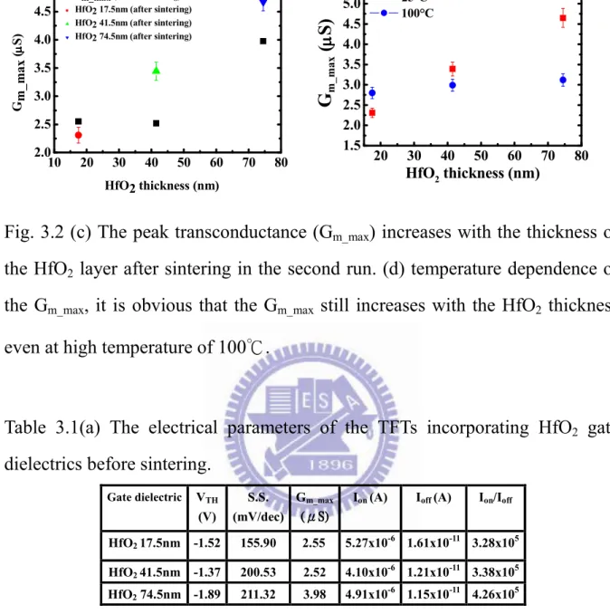
Table 3.1 (a) The electrical parameters of the TFTs incorporating HfO2 gate
dielectrics before sintering………..43
Table 3.1 (b) The electrical parameters of the TFTs incorporating HfO2 gate
dielectrics after sintering……….43
Table 3.2 The initial peak transconductance and the modified peak transconductance……….48
Chapter 4
Table 4.1 The material composition of the transition layer in the 250Ǻ sample, it is observed that the transition layer is mainly composed of Al and O atoms…..72 Table 4.2 The material composition of the transition layer in the 1700Ǻ sample, it is observed that the transition layer is mainly composed of Al and O atoms..72
Figure Caption
Chapter 1Fig. 1.1 The schematic plot of the NBTI stress mechanism in the TFTs
with SiO2 gate dielectrics………...11
Fig. 2.1 The device fabrication of the HfO2-poly-Si TFTs………..30
Chapter 3
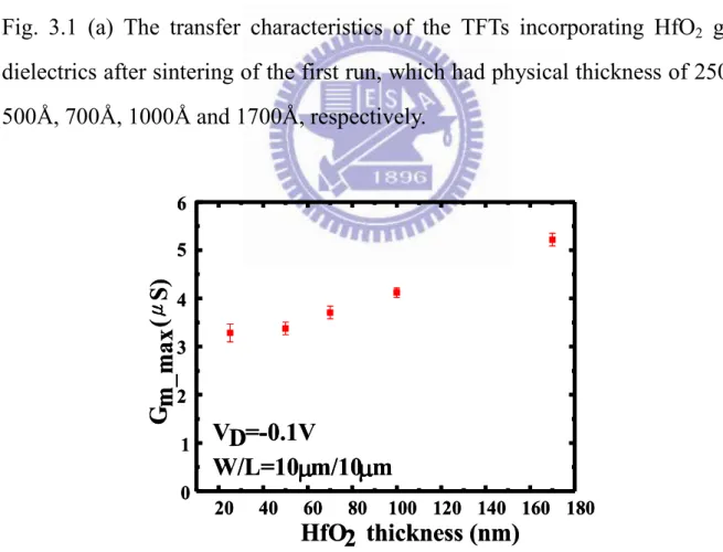
Fig. 3.1 (a) The transfer characteristics of the TFTs incorporating HfO2 gate
dielectrics after sintering of the first run, which had physical thickness of 250Å, 500Å, 700Å, 1000Å and 1700Å, respectively………41
Fig. 3.1 (b) The peak transconductance (Gm_max) increases with the thickness of
the HfO2 layer in the first run………..41
Fig. 3.2 (a) The transfer characteristics of the TFTs incorporating HfO2 gate
dielectrics before sintering at 400℃ in a N2 ambient of the second run, which
had physical thickness of 175Å, 415Å and 745Å, respectively………..42
Fig. 3.2 (b) The transfer characteristics of the TFTs incorporating HfO2 gate
dielectrics after sintering at 400℃ in a N2 ambient of the second run, which had
physical thickness of 175Å, 415Å and 745Å, respectively……….42
Fig. 3.2 (c) The peak transconductance (Gm_max) increases with the thickness of
the HfO2 layer after sintering in the second run. (d) temperature dependence of
the Gm_max, it is obvious that the Gm_max still increases with the HfO2 thickness
even at high temperature of 100℃………..43
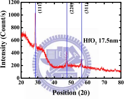
Fig. 3.3 (a) The peak positions and intensities of the XRD spectra for three main crystalline phase of HfO2, obtained from powder diffraction ICDD card files..44
Fig. 3.3 (b) XRD spectra of the 175Å-thick HfO2 layer, showing the clear peaks
correspond to the monoclinic phase in the Fig. 3-3 (a), indicating that the phase transformation completes after sintering at 400℃in a N2 ambient……….44
Fig. 3.3 (c) XRD spectra of the 415Å-thick HfO2 layer. No obvious peak was
observed, indicating that the phase remains amorphous after sintering at 400℃ in a N2 ambient………45
Fig. 3.3 (d) XRD spectra of the 745Å-thick HfO2 layer. No obvious peak was
observed, indicating that the phase remains amorphous after sintering at 400℃ in a N2 ambient………45
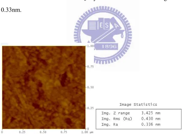
Fig. 3.4 (a) The atomic-force microscopy (AFM) image of the poly-Si surface of the TFTs with 250Å-thick HfO2 layer. The mean surface roughness is about
0.33nm……….46
Fig. 3.4 (b) The atomic-force microscopy (AFM) image of the poly-Si surface of the TFTs with 1700Å-thick HfO2 layer. The mean surface roughness is about
0.43nm………...46
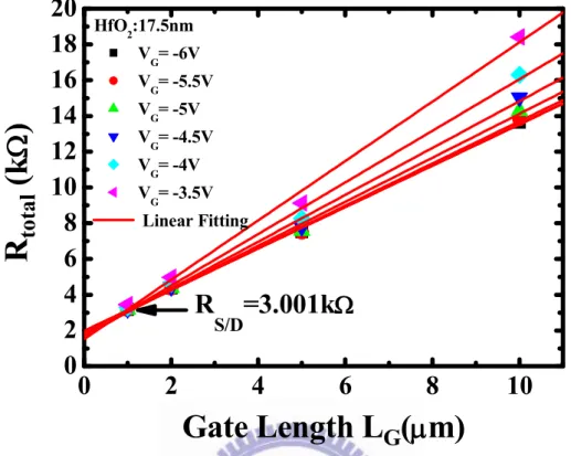
Fig. 3.5 (a) The extraction of the source/drain sheet resistance of the TFTs incorporating the 175Å-thick HfO2 gate dielectric……….47
Fig. 3.5 (b) The extraction of the source/drain sheet resistance of the TFTs incorporating the 415Å-thick HfO2 gate dielectric……….47
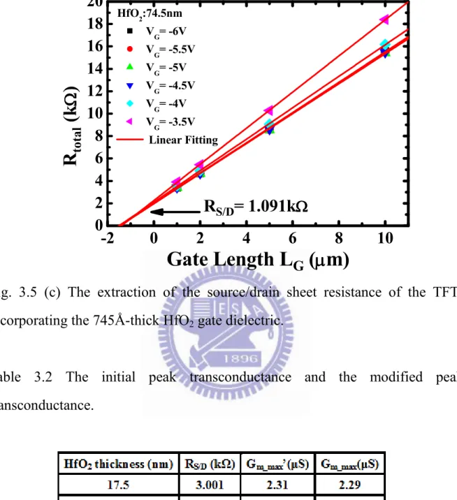
Fig. 3.5 (c) The extraction of the source/drain sheet resistance of the TFTs incorporating the 745Å-thick HfO2 gate dielectric……….48
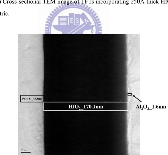
Fig. 3.6 (a) Cross-sectional TEM image of TFTs incorporating 250Å-thick HfO2
gate dielectric……….…..49
Fig. 3.6 (b) Cross-sectional TEM image of TFTs incorporating 1700Å-thick HfO2 gate dielectric……….49
Fig. 3.7Schematic of the silicon-metal oxide stack, showing the mechanism of transport of oxygen from the ambient to the silicon interface……….50
Fig. 3.8 It become easier for holes to get across the grain boundary potential barrier height after the grain boundary potential barrier height is lowered by the
voltage drop induced by the positively charged oxygen vacancies……….50
Chapter 4
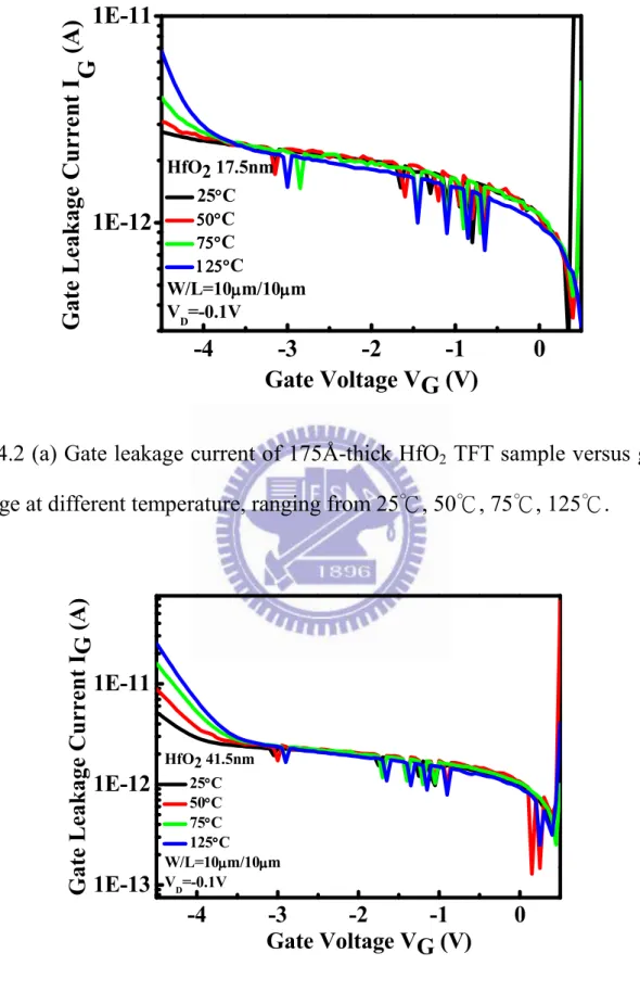
Fig. 4.1 Gate leakage current versus gate voltage of at 25℃………..71
Fig. 4.2 (a) Gate leakage current of 415Å-thick HfO2 TFT sample versus gate
voltage at different temperature, ranging from 25℃, 50℃, 75℃, 125℃……...73
Fig. 4.2 (b) Gate leakage current of 415Å-thick HfO2 TFT sample versus gate
voltage at different temperature, ranging from 25℃, 50℃, 75℃, 125℃……...73
Fig. 4.2 (c) Gate leakage current of 745Å-thick HfO2 TFT sample versus gate voltage at different temperature, ranging from 25℃, 50℃, 75℃, 125℃……...74
Fig. 4.3 The schematic plot of the Vth contribution separating method. We can
derive the Vth shift attributed to oxide trapping by shifting the Von of the initial
ID-VG curve to the Von of the ID-VG curve after stressing. On the other hand, we
can derive the Vth shift attributed to the interface states generation after shifting
the Von of the initial ID-VG curve……….74
Fig. 4.4 (a) The total Vth shift of TFTs with 175Å, 415Å and 745Å-thick HfO2
gate dielectrics versus stress time at VG_stress - Vth = -3V from 2 to 1000 seconds
Fig. 4.4 (b) The Vth shift resulted from oxide trapping of TFTs with 175Å, 415Å
and 745Å-thick HfO2 gate dielectrics versus stress time at VG_stress - Vth = -3V
from 2 to 1000 seconds at 25℃………...75 Fig. 4.4 (c) The Vth shift resulted from interface states of TFTs with 175Å, 415Å
and 745Å-thick HfO2 gate dielectrics versus stress time at VG_stress - Vth = -3V
from 2 to 1000 seconds at 25℃……….…..76 Fig. 4.4 (d) The S.S. degradation of TFTs with 175Å, 415Å and 745Å-thick HfO2 gate dielectrics versus stress time at VG_stress - Vth = -3V from 2 to 1000
seconds at 25℃………...….76 Fig. 4.4 (e) The Gm_max degradation of TFTs with 175Å, 415Å and 745Å-thick
HfO2 gate dielectrics versus stress time at VG_stress - Vth = -3V from 2 to 1000
seconds at 25℃………77 Fig. 4.4 (f) The trap state generation of TFTs with 175Å, 415Å and 745Å-thick HfO2 gate dielectrics at VG_stress - Vth = -5V after tress time of 1000 seconds at
25℃.………77 Fig. 4.4 (g) Schematic energy band diagram and the schematic degradation mechanism of the 175Å-thick HfO2 TFTs during NBTI stress with
VG_stress-Vt=-5V at 25 ℃……….….78
Fig. 4.4 (h) Schematic energy band diagram and the schematic degradation mechanism of the 415Å-thick HfO2 TFTs during NBTI stress with
VG_stress-Vt=-3V at 25℃………...78
Fig. 4.4 (i) Schematic energy band diagram and the schematic degradation mechanism of the 745Å-thick HfO2 TFTs during NBTI stress with
VG_stress-Vt=-3V at 125℃……….79
Fig. 4.5 (a) The total Vth shift of TFTs with 175Å, 415Å and 745Å-thick HfO2
gate dielectrics versus stress time at VG_stress - Vth = -5V from 2 to 1000 seconds
at 25℃……….79 Fig. 4.5 (b) The Vth shift resulted from oxide trapping of TFTs with 175Å, 415Å
and 745Ǻ-thick HfO2 gate dielectrics versus stress time at VG_stress - Vth = -5V
from 2 to 1000 seconds at 25℃………..80 Fig. 4.5 (c) The Vth shift resulted from interface states of TFTs with 175Å, 415Å
and 745Å-thick HfO2 gate dielectrics versus stress time at VG_stress - Vth = -5V
from 2 to 1000 seconds at 25℃………...80 Fig. 4.5 (d) The S.S. degradation of TFTs with 175Å, 415Å and 745Å-thick HfO2 gate dielectrics versus stress time at VG_stress - Vth = -5V from 2 to 1000
seconds at 25℃………81 Fig. 4.5 (e) The Gm_max degradation of TFTs with 175Å, 415Å and 745Å-thick
HfO2 gate dielectrics versus stress time at VG_stress - Vth = -5V from 2 to 1000
seconds at 25℃………81 Fig. 4.5 (f) The trap state generation of TFTs with 175Å, 415Å and 745Å-thick HfO2 gate dielectrics at VG_stress - Vth = -5V after tress time of 1000 seconds at
25℃……….82 Fig. 4.5 (g) Schematic energy band diagram and the schematic degradation mechanism of the 175Å-thick HfO2 TFTs during NBTI stress with
VG_stress-Vt=-5V at 25 ℃………..82
mechanism of the 415Å-thick HfO2 TFTs during NBTI stress with
VG_stress-Vt=-5V at 25℃………...83
Fig. 4.5 (i) Schematic energy band diagram and the schematic degradation mechanism of the 745Å-thick HfO2 TFTs during NBTI stress with
VG_stress-Vt=-5V at 25℃………...83
Fig. 4.6 (a) The total Vth shift of TFTs with 175Å, 415Å and 745Å-thick HfO2
gate dielectrics versus stress time at VG_stress - Vth = -3V from 2 to 1000 seconds
at 125℃………...84 Fig. 4.6 (b) The Vth shift resulted from oxide trapping of TFTs with 175Å, 415Å
and 745Å-thick HfO2 gate dielectrics versus stress time at VG_stress - Vth = -3V
from 2 to 1000 seconds at 125℃……….84 Fig. 4.6 (c) The Vth shift resulted from interface states of TFTs with 175Å, 415Å
and 745Ǻ-thick HfO2 gate dielectrics versus stress time at VG_stress - Vth = -3V
from 2 to 1000 seconds at 125℃……….85 Fig. 4.6 (d) The S.S. degradation of TFTs with 175Å, 415Å and 745Å-thick HfO2 gate dielectrics versus stress time at VG_stress - Vth = -3V from 2 to 1000
seconds at 125℃………..85 Fig. 4.6 (e) The Gm_max degradation of TFTs with 175Å, 415Å and 745Å-thick
HfO2 gate dielectrics versus stress time at VG_stress - Vth = -3V from 2 to 1000
seconds at 125℃………..86 Fig. 4.6 (f) The trap state generation of TFTs with 175Å, 415Å and 745Å-thick HfO2 gate dielectrics at VG_stress - Vth = -3V after tress time of 1000 seconds at
Fig. 4.6 (g) Sechematic energy band diagram and the schematic degradation mechanism of the 175Å-thick HfO2 TFTs during NBTI stress with
VG_stress-Vt=-3V at 125℃……….87
Fig. 4.6 (h) Sechematic energy band diagram and the schematic degradation mechanism of the 415Å-thick HfO2 TFTs during NBTI stress with
VG_stress-Vt=-3V at 125℃……….87
Fig. 4.6 (i) Schematic energy band diagram and the schematic degradation mechanism of the 745Å-thick HfO2 TFTs during NBTI stress with
VG_stress-Vt=-3V at 125℃……….88
Fig. 4.7 (a) The total Vth shift of TFTs with 175Å, 415Å and 745Å-thick HfO2
gate dielectrics versus stress time at VG_stress - Vth = -4V from 2 to 1000 seconds
at 125℃………...88 Fig. 4.7 (b) The Vth shift resulted from oxide trapping of TFTs with 175Å, 415Å
and 745Å-thick HfO2 gate dielectrics versus stress time at VG_stress - Vth = -4V
from 2 to 1000 seconds at 125℃……….89 Fig. 4.7 (c) The Vth shift resulted from interface states of TFTs with 175Å, 415Å
and 745Å-thick HfO2 gate dielectrics versus stress time at VG_stress - Vth = -4V
from 2 to 1000 seconds at 125℃……….89 Fig. 4.7 (d) The S.S. degradation of TFTs with 175Å, 415Å and 745Å-thick HfO2 gate dielectrics versus stress time at VG_stress - Vth = -4V from 2 to 1000
seconds at 125℃……….90 Fig. 4.7 (e) The Gm_max degradation of TFTs with 175Å, 415Å and 745Å-thick
seconds at 125℃………..90 Fig. 4.7 (f) The trap state generation of TFTs with 175Å, 415Å and 745Å-thick HfO2 gate dielectrics at VG_stress - Vth = -4V after tress time of 1000 seconds at
125℃………...91 Fig. 4.7 (g) Schematic energy band diagram and the schematic degradation mechanism of the 175Å-thick HfO2 TFTs during NBTI stress with
VG_stress-Vt=-4V at 125℃……….91
Fig. 4.7 (h) Schematic band diagram and the schematic degradation mechanism of the 415Å-thick HfO2 TFTs during NBTI stress with VG_stress-Vt=-4V at
125℃………...92 Fig. 4.7 (i) Schematic energy band diagram and the schematic degradation mechanism of the 745Å-thick HfO2 TFTs during NBTI stress with
VG_stress-Vt=-4V at 125℃……….92
Chapter 1
Introduction
1.1 Overview of Thin-Film Transistors
A thin-film transistor (TFT) is a special type of field-effect transistor made
by depositing thin films of a semiconductor active layer as well as the dielectric layer and metallic contacts over a substrate. A common substrate is glass, since the primary application of TFTs is in liquid crystal displays. This is different from the conventional transistor where the substrate material is typical semiconductor material, such as a silicon wafer. The first TFT device was proposed in 1961 by Dr. P.K. Wenimer in Radio Company of America (RCA). In 1966, the first polycrystalline silicon thin film transistors (Poly-Si TFTs) were demonstrated by C.H. Fa et al [1]. However, the study of poly-Si TFTs fabricated with low temperature of 600℃ was not proposed until 1980s. With its simplicity of structure and fabrication, the low-temperature polycrystalline silicon TFT (LTPS-TFT) has drawn much attention for the application in image sensors and displays. In recent years, the flat panel display (FPD) is widely used in advanced electronic products such as mobile phones, portable computers, digital cameras and PDA, etc. In all types of flat panel displays, active matrix liquid crystal display is the most popular type of FPD due to its higher refresh rate compared with the conventional passive matrix display [2]-[3]. Besides, LTPS-TFTs have been exhibited in a variety of industrial applications, such as active matrix liquid crystal displays (AMLCDs) [2]-[4], active matrix organic light emitting displays (AMOLEDs) [5]-[7], high density static random access
memories (SRAMs) [8], electrical erasable programming read only memories (EEPROM) [9]-[10], and 3D ICs’ applications [11].
It has been known that the hydrogenated amorphous silicon (a-Si) TFTs were widely used for the pixel switching devices of AMLCDs . The advantages of a-Si:H TFTs are their thermal compatibility with low temperature process on large area glass substrates and high off-stated which results in low leakage current. However, the low electron mobility typically below 1cm2V-1sec-1 will limit the performance for AMLCD applications. Consequently, the invention of poly-Si-TFTs will suppress the limitation of a-Si:H TFTs to derive higher field effect mobility due to its larger grain size of poly-grains. The high field effect mobility and drive current of poly-Si-TFTs make it possible to use them as the switching pixels and driver circuits [12]. What’s more, the aperture ratio and the panel brightness can be also prompted a lot because that there is just a small size of device needed by utilizing LTPS-TFTs [13]. Therefore, the performance of displays can be improved and thus the poly-Si -TFTs have a great potential to realize the high-performance large-area AMLCDs and system on panels (SOP). However, the low temperature process is necessary because the switch pixels are required to be embedded on the glass substrates for the applications of FPD. Generally the melting point of glass is about 660℃,so the maximum process
temperature of poly-Si TFTs must be controlled below 600℃ to avoid the glass substrate melting. Furthermore, the formation of gate insulator and the dopant activation are also limited by the low-temperature process. Hence, a new low temperature process of poly-Si TFTs is needed to make the poly-Si TFTs possible to be compatible to the industrial requirements.
strongly related to the grain boundaries between the poly-grains and the intra-granular defects in the grains. The grain boundaries consist of large amount of dangling bonds and strained bonds [14]. These imperfect bondings will trap mobile carriers in the channel and become charged to result in a high potential barrier at these locations. So the carrier mobility and subthreshold swing will be severely degraded in the poly-Si TFTs. Moreover, the grain boundaries also provide the paths of leakage current to enhance the standby power consumption. In order to obtain higher drive current and lower leakage current of LTPS-TFTs, the most import thing is to enlarge the grain size of poly-Si so that the grain boundary density will be reduced [15]. Generally speaking, growing poly-Si by low temperature chemical vapor deposition (LPCVD) will obtain the small size of poly-grains and result in a poor electrical performance of devices. However, re-crystallization of a-Si will get larger poly-grain size than growing poly-Si directly. For achieving this goal, variety methods were proposed to re-crystallize the a-Si films such as SPC (solid phase crystallization) [16]. ELA (excimer laser annealing) [17], and MILC (metal induced lateral crystallization) [18] to obtain the large grain size of poly-Si and thus enhance the field effect mobility. Apart from the method of re-crystallization of a-Si, lots of plasma treatment methods are also proposed to passivate the trap states in grain boundaries. Several plasma sources such as H2 [19], NH3 [20], N2O [21] and O2 [22] plasma have been
widely investigated recently.
1.2 Poly-Si TFTs using High-k Gate Dielectrics
have been widely used in active-matrix liquid crystal displays (AMLCD) with integrated peripheral circuits as the pixel array on the glass substrate because of their superior performance [23]. Recently, the practicability of integrating the entire system on panels (SOP) has been proposed successfully [24]. To fulfill this goal, it requires that the display driving circuits contain LTPS-TFTs are capable of operating at low voltages while delivering high drive currents. Traditionally, we use silicon dioxide (SiO2) as the gate dielectric materials in
LTPS-TFTs. However, with the scaling down of the gate oxide thickness to obtain the higher drive current and better gate control ability, SiO2 encounters
many problems including high gate leakage current [25]. Consequently, to maintain the physical dielectric thickness while increasing the gate capacitance, the conventional SiO2 gate dielectric layer must be replaced with a material that
offers a higher dielectric constant κ than SiO2, several new high-k materials have
been proposed including Al2O3, Ta2O5 and HfO2 [26]-[28]. Among these high-k
materials, HfO2 has been viewed as the most appropriate high-κ dielectrics for
the TFTs due to its high value of κ (14 to 20) , wide band-gap (~ 5.8eV) and excellent thermal stability in contact with poly-Si [29]-[30]. Hf oxide and Hf silicate thin films, currently being considered for gate dielectric applications result in a multilayer structure that includes a SiO2-like layer either
spontaneously or intentionally formed at the interface with the substrate [31].
1.3 Negative Bias Temperature Instability of LTPS TFTs
Negative bias temperature instability (NBTI) mainly occurs in the p-channel devices. During negative bias stress at elevated temperature (typically
100℃-150℃), several important electrical parameters such as threshold voltage (Vth), driving current (ID), carrier mobility and the peak transconductance (Gm)
of the device will be severely degraded [32]-[33]. The degradation of these device parameters can lead to circuit failures, both for analog and digital applications.
The NBTI induced degradation is mainly attributed to interface states and fixed oxide charges and it can be thermally and electrically activated. The NBTI stress has been widely investigated in the p-channel TFTs and the reaction-diffusion (R-D) model [34]-[35] has been used to explain the phenomenon of NBTI stress in p-channel TFTs and the physical model of NBTI stress is shown in the Fig. 1.1. The NBTI-degradation mechanism of p-channel TFTs is described as follows [32]:
It is assumed that the Si dangling bonds at the poly-Si/SiO2 interface are
passivated by the hydrogen atoms in the horizontal furnace initially. During the NBTI stress, the inversion holes will react with the Si-H bonds at the poly-Si/SiO2 interface and in the grain boundaries, and then the hydrogen atoms
of the Si-H bonds become weakly bonded to the Si atoms. Thus, the hydrogen atoms can be easily released from the weak Si-H bonds by sufficient thermal energy. The release of hydrogen results in the generation of interface states and grain boundary trap states. The released hydrogen related species from the interface either diffuse or drift into the gate oxide and react with it, forming OH groups bounded to Si atoms of oxide and leaving positive fixed oxide charges behind in the gate oxide, becoming the reacting-limiting factor.
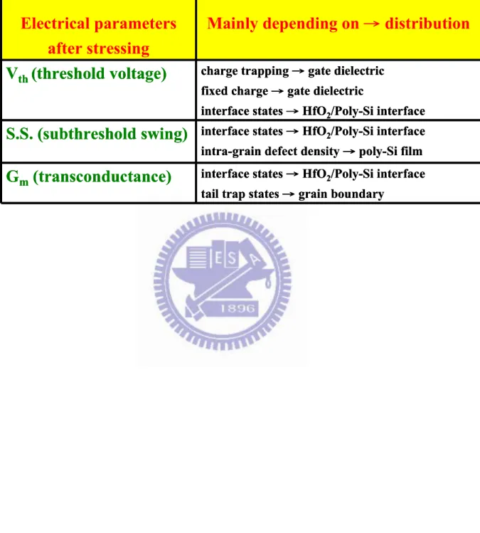
parameters during NBTI stress, we have to understand every possible factor that contributes to the degradation of electrical parameters in TFTs. In poly-Si TFTs, unlike the fundamental theory of MOSFETs, the electrical parameters such as threshold voltage (Vth), subthreshold swing (S.S.) and transconductance (Gm) are
all dependent on the generation of interface states and trap states at the interface and/or in the grain boundaries. Based on the degradation mechanism of poly-Si TFTs, the main degradation mechanism of the electrical parameters of poly-Si TFTs will be described as follows: The generation of fixed oxide charge and charge trapping in the gate dielectric will cause the Vth shift. The interface states
would contribute to Vth shift and degrade the subthreshold swing (S.S.) and
transconductance (Gm). The trap states generated in the TFTs are usually divided
into two types and their effects on the electrical performance are different [36]-[37]. (1) deep trap states : Deep trap state is a type of trap states that located in the mid-gap of the silicon energy level. The deep trap states are usually caused by the dangling bonds (defects) at the HfO2/poly-Si interface or in the
grain of the poly-Si channel film. The generation of deep trap states would severely cause the Vth shift and degrade the subthrethold swing (S.S.) , whereas
it has little effect on the transconductance (Gm) (2) tail trap states: the tail trap
state is one type of trap states that located near the conduction band or the valence band edge of the silicon energy level. The tail trap states are attributed to the strained bonds at the poly-Si/IL interface or in the grain boundary trap states. The generation of tail trap states would severely contribute to the degradation of the transconductance (Gm), whereas it has little impact on the
subthrethold swing (S.S.). The degradation of the electrical parameters after stress discussed above will help us to clarify the generation and distribution of defects and trap states of LTPs TFTs. These proposed mechanisms are
summarized in the Table 1.
1.4 NBTI Stress in High-κ Gate Dielectrics
It is generally recognized that HfO2 layer has a significant larger amount of
bulk traps than that in SiO2. The presence of bulk traps complicates the
mechanism of NBTI further [38]. Charge trapping characteristics of HfO2
MOSFETs were affected by the process conditions. One factor is the thickness of the HfO2 layer. It was observed that the charge trapping was enhanced for the
thicker HfO2 layer [39]. Charge trapping is dominant in the thick films and
dominates the generation of interface traps that are formed during the stress. The oxide trapped charge at the interface between the dielectric and the substrate is recognized to make the most significant contribution to Vth [40]. It was also
reported that the charge trapping is related to the neutral HfOH centers, indicating that the charge trapping in the HfO2 layer is hydrogen-related [41].
Huard et al. [42] reports that the Vth shift contributed by charge trapping is
composed of two steps: firstly, hole traps (meta-stable states) which recover, and interface states (Pb0) which are stable (no recovery). It was also reported that the
mechanism taking place in the NBTI stress is described as follows: The hydrogen release induces interface states and the holes will be captured by the oxide traps [43]. The observed similarities between high-κ gate dielectrics and nitride silicon dioxide [43] tell us that the property of the interfacial layer between the HfO2 and the substrate is very close to the amorphous silicon
dioxide, so the mechanism of NBTI stress in SiO2 MOSFETs will help us to
1.5 Mobility Issues in High-k Dielectrics
High-permittivity dielectrics, as an alternative of conventional SiO2 gate
oxide, are widely investigated in metal-oxide-semiconductor (MOS) devices for their capability to reduce gate leakage current for the same electrical capacitance [44]-[45]. Among all the candidates for high-κ gate dielectrics, Hf-based oxides, such as HfO2 or HfSixOy have attracted much attention. However, there are
many issues to be studied and solved for these new materials. Among the issues raised by the integration of high-κ materials, the degradation of carrier mobility for the metal gate/high-κ gate stacks remains one of the most serious issues [46]. The degradation is attributed to intrinsic properties of high-κ materials such as fixed charges induced remote coulomb scattering [47], remote surface roughness scattering [48], remote soft-optical phonon scattering (RPS) [49], interfacial dipole scattering [50] and crystallization [51].
Recently, high-κ materials are not only used in the complementary metal-oxide-semiconductor (CMOS) process but also studied in the poly-silicon thin film transistors. By using the high-κ gate dielectrics, we can preserve the physical gate-dielectric thickness while increasing the gate capacitance density and then improving the mobile carrier density in the channel region.[52]-[54] .
1.6 Motivation
As far as we know, the gate capacitance is inversely proportional to the thickness of the gate dielectrics. That is to say, the thinner gate dielectric will result in the higher peak transconductance (Gm_max). However, the Gm_max of the
TFT devices using HfO2 gate dielectrics increases with the HfO2 thickness in our
work. This phenomenon is contrary to the knowledge we had before. As a result, it is interesting and worthwhile to find out the main cause of this phenomenon.
Apart from the investigation on the electrical characteristics of the TFTs with different HfO2 thickness, the NBTI stress is also studied to compare the
Table 1.1 Variation of electronic parameters and corresponding possible degradation mechanism and the main degraded locations.
interface states →→→→ HfO2/Poly-Si interface tail trap states →→→→ grain boundary
G
m(transconductance)
interface states →→→→ HfO2/Poly-Si interface intra-grain defect density →→→ poly-Si film→
S.S. (subthreshold swing)
charge trapping →→→→ gate dielectric fixed charge →→→→ gate dielectric
interface states →→→→ HfO2/Poly-Si interface
V
th(threshold voltage)
Mainly depending on →
→
→
→ distribution
Electrical parameters
after stressing
Fig. 1.1 The schematic plot of the NBTI stress mechanism in the TFTs
Reference
Chapter 1
[1] C. H. Fa, and T. T. Jew, “The polysilicon insulated-gate field-effect transistor,” IEEE Trans. Electron Devices, vol. 13, no. 2, pp. 290, 1966.
[2] R. E. Proano, R. S. Misage, D. Jones, D. G. Ast, “Guest-host active matrix liquid-crystal display using high-voltage polysilicon thin film transistors,” IEEE Trans. Electron Devices, vol.38, no. 8, pp. 1781-1786, Aug. 1991.
[3] Y. Oana, “Current and future technology of low temperature poly-Si TFT-LCDs,” J. Soc. Inf. Disp., 9, pp. 169, 2001.
[4] S. Morozumi, K. Oguchi, S. Yazawa, Y. Kodaira, H. Ohshima, and T. Mano, “B/W and color LC video displays addressed by poly-Si TFTs,” SID Dig., pp. 156, 1983.
[5] M. Stewart, S. Pobert. Howell, Leo Pires, Miltiadis K. Hatalis, Webester Howard, and Olivier Prache, “Polysilicon VGA active matrix OLED displays – technology and performance,” in IEDM tech, Dig., 1998, pp. 871-874.
[6] Mark Stewart, Pobert S. Howell, Leo Pires, Miltiadis K. Hatalis, “Polysilicon TFT technology for active matrix OLED displays, “IEEE Trans. Electron Device, vol. 48, pp. 845-851, 2001.
displays realized using metal-induced unilateral crystallized polycrystalline silicon thin-film transistors,” IEEE Trans. Electron Devices, vol. 49, pp. 991-996, 2002.
[8] S. Batra, “development of drain-offset (DO) TFT technology for high density SRAM’s,” Extended Abstracts, vol.94-2, in Electrochemical Soc. Fall Mtg., Miami Beach, FL, Oct. pp. 677, 1994.
[9] M. Cao, et al., “A simple EEPROM cell using twin polysilicon thin-film transistors,” IEEE Trans. Electron Devices, vol. 15, pp. 304, 1994.
[10] N. D. Young, G. Harkin, R. M. Bunn, D. J. McCulloch, and I. D. French, “The fabrication and characterization of EEPROM arrays on glass using a low temperature poly-Si TFT process,” IEEE Trans. Electron Devices, vol. 43, pp. 1930-1936, 1996.
[11] K. Banerjee, S. J. Souri, P. Kapur, and K. C. saraswat, “3-D ICs: a novel chip design for improving deep-submicrometer interconnect performance and system-on-chip integration, “ Proceedings of the IEEE, vol. 89, pp. 602-633, 2001.
[12] W. G. Hawkins, “Polycrystalline-silicon device technology for large-area electronics, “ IEEE Trans. Electron Devices, vol. 33, pp. 477-481, 1996.
[13] I. Wu, “Cell design considerations for high-apeture-ratio direct-view and projection polysilicon TFT-LCDs,” in SID Tech. Dig., pp. 19, 1995.
[14] S. Seki, O. Kogure, and B. Tsujiyama, “Effects of crystallization on trap state densities at grain boundaries in polycrystalline silicon, ” IEEE
Electron Device Lett., vol. 18, no. 8, pp. 368-370, 1987.
[15] H. Kuriyama et al., “Enlargement of poly-Si film grain size by excimer laser annealing and its application on high-performance poly-Si thin film transistor,” Jpn. J. Appl. Phys., vol. 30, pp. 3700-3703, 1991.
[16] W. Little, K. I. Takahara, H. Koike, T. nakazawa, I. Yudasaka, and H. Ohshima, “ Low temperature poly-Si TFTs using solid phase crystallization of very thin films and an electron resonance chemical vapor deposition gate insulator,” Jpn. J. Appl. Phys., vol. 30, no. 12B, pp. 3724, 1991.
[17] H. Kuriyama, S. Kiyama, S. Nouguchi, “ Enlargement of poly-Si film grain size by excimer laser annealing and its application to high-performance poly-Si thin film transistor,“ Jpn. J. Appl. Phys., vol.30, no. 12B, pp. 3700-3703, 1991.
[18] S. W. Lee and S. K. Joo,” Low temperature poly-Si thin-film transistors fabrication by metal-induced lateral crystallization,” IEEE Electron Device Lett., vol. 17, no. 4, pp. 160-162, 1996.
[19] A. Yin, and S. J. Fonash, “ High-performance p-channel poly-Si TFT’s using electron cyclotron resonance hydrogen plasma passivation,” IEEE Electron Device Lett., vol. 15, no. 12, pp. 502-503, 1994.
[20] C. K. Yang, T.F. Lei, C. L. Lee, “The combined effects of low pressure NH3 annealing and H2 plasma hydrogenation on polysilicon
thin-film-transistors,” IEEE Electron Device Lett., vol. 15, pp. 389-390, 1994.
[21] J. W. Lee, N. I. Lee, J. I. Kan, C.H. Han, ”Characterization of polysilicon thin-film transistor with thin-gate dielectric grown by electron cyclotron resonance nitrous oxide plasma,” IEEE Electron Device Lett., vol. 18, pp. 172-174, 1997.
[22] K. C. Moon, J. H. Lee, M. K. Han, “Improvement of polycrystalline silicon thin film transistor using oxygen plasma pretreatment before laser crystallization,” IEEE Trans. Electron Devices, vol. 49, pp. 1319, 2002.
[23] H. Oshima and S. Morozumi. “Future trends for TFT integrated circuits on glass substrates, “ in IEDM Tech .Dig., 1989, pp. 157-160.
[24] K. Wener, “The flowering of flat displays,” IEEE Spectrum, vol. 34, no. 5. pp. 40-49, May 1997.
[25] A. Takami, A. Ishida, J. Tsutsumi, T. Nishibe, and N. Ibaraki,“Threshold voltage shift under the gate bias stress in low-temperature poly-silicon TFT with the thin gate oxide film,” in Proc. Int. Workshop AM-LCD, Tokyo , Japan, Jul. 2000, pp. 45-58.
[26] M. Y. Um, S. K. Lee, and H. J. Kim, “Characterization of thin film transistor using Ta2O5 gate dielectric,” in proc. Int. Workshop AM-LCD,
Tokyo, Japan, Jul. 1998, pp. 45-46.
[27] Z. Jin, .S. Kwok, and M. Wong, “High-performance polycrystalline SiGe thin-film transistors using Al2O3 gate insulators,” IEEE Electron
Device Lett., vol. 19, no. 12, pp. 502-504, Dec. 1998.
“High-Performance poly-Silicon TFTs using HfO2 gate dielectric,” IEEE
Electron Device Lett,” vol. 27. no. 5, May. 2006.
[29] C. Hobbs, H. Tseng, K. Reid, B. Taylor, L. Herbert, R. Garcia, R. Hegde, J. Grant, D. Gilmer, A. Franke, V. Dhandapani, M .Azrak, L. Prabhu, R. Rai, S. Bachi, J. conner ,S. Backer, F. Dumbuya, B. Nguyen, and P, Tobin, ”80nm poly-Si gate CMOS with HfO2 gate dielectric,” in IEDM Tech. Dig., 2001, pp. 651-654.
[30] Y. Kim, C. Lim, C. D. Young, K. Mathews ,J. Barnett ,B. Foran, A. Agarwal, G. A. Brown, G. Bersuker, P. Zeitzoff, M. Gardner, R. W. Murto, L. Larson, C. Metzner, S. Kher, and H. R. Huff, “Conventional poly-Si gate MOS transistors wit ha novel, ultra thin Hf-oxide layer,” in VLSI Symp. Tech. Dig., 2003, pp. 167-168.
[31] M. J. Yang, C. H. Chien, Y. H. Lu, C. Y. Shen, and T. Y. Huang,”Electrical properties of low-temperature-compatible p-channel polycrystalline-silicon TFTs using high-κ gate dielectrics,” IEEE Trans. Electron Devices, vol. 55, no. 4, Apr. 2008.
[32] C.Y. Chen, J.W. Lee, S.D. Wang, M.S. Shieh, P.H. Lee, W.C. Chen, H.Y. Lin K.L. Yeh, T.F. Lei, “Negative bias temperature instability on low-temperature polycrystalline silicon thin-film transistors,” IEEE Trans. Electron Devices, vol. 53, no. 12, pp. 2993-3000, 2006.
[33] C. Y. Chen, M. W. Ma, W. C. Chen, H. Y. Lin, K. L. Yeh, S. D. Wang, T. F. Lei, “Analysis of negative bias temperature instability in body-Tied low-temperature polycrystalline silicon thin-film transistors,“ IEEE
Electron Device Lett., vol. 29, no. 2, pp. 165-167, 2008.
[34] S. Mahapatra, P. B. Kumar, and M.A. Alam, “Investigation and modeling of interface and bulk trap generation during negative bias temperature instability of pMOSFETs,” IEEE Trans. Electron Devices, vol. 51, no. 6, pp. 1371-1379, 2004.
[35] A. T. Krishnan, S. Chakravarthi, P. Nicollian ,V. Reddy, S. Krishinan, “Negative bias temperature instability mechanism: The role of molecular hydrogen,” Appl, Phys, Lett., no. 88, 153518, 2006.
[36] I-W. Wu, Y-Y. Huang, W. B. Jackson, A. G. Lewis, and A. C. Chiang, “ Passivation kinetics of two types of defects in polysilicon TFT by plasma hydrogenation,” IEEE Electron Device Lett, vol. 12, pp. 181-183, 1991.
[37] G. A. Armstrong, S. Uppal, S. D. Brotherton, and J. R. Ayres, “ Differentiation of effects due to grain and grain boundary traps in laser annealed poly-Si film transistors,” Jpn. J. Appl. Phys.,vol. 37, pp. 1721-1726, 1998.
[38] Harris HR, Choi R, Lee BH, Young CD, Sim JH, Mathews K, Zeitzoff P, Majhi P, Bersuker G: Comparison of NMOS and PMOS stress for determining the source of NBTI TiN/HfSiON devices. In: IRPS: 2005; San Jose Ca; 2005: 80-83.
[39] K. Onishi, C. S. Kang, R. Choi, H-J. Cho, S. Gopalan, R. Nieh, S. Krishnan, and J. C. Lee, „ Charging effects on reliability of HfO2
419-420.
[40] E. H. Nicollian and J. R. Brews, MOS Physics and Technology. New York : Wiley, 1991.
[41] K. Onishi, R. Choi ,C. S. Kang , H-J. Cho, Y. H. Kim, R. E. Nieh, J. H. Siddharth, A. Kirshnan, M. S. Akbar, and J. C. Lee. “Bias-temperature instability of polysilicon gate HfO2 MOSFETs,”
IEEE, Trans, Electron Devices., vol. 50, no. 6, Jun. 2003.
[42] V. Huard, F. Monsieur ,G. Ribes, and S. Bruyere, “Evidence for hydrogen-related defects during NBTI stress in p-MOSFETs,” in Proc, Int. Reliability Physics Symp., 2003, pp. 178-182.
[43] G. Ribes, J. Mitard, M. Denais, s. Bruyeree, F. Monsieur, C. Parthasarathy, E.Vincent, and G. Ghibaudo,”Review on High-κ dielectrics reliability issues,” IEEE, Trans, Device and Materials Reliability., vol. 5, no. 1, Mar. 2005.
[44] M. Fischetti, “Scaling MOSFETs to the limit: A physicist’s perspective,” J. Comput. Electron., vol. 2, no. 2-4, pp. 73-79, 2003.
[45] G. Bersuker, P. Zeitzoff, G. Brown, and H. Huff, “Dielectrics for future transistors,” Mater. Today, vol. 7, no. 1, pp. 26-33, 2004.
[46] S. Saito, K. Torii, Y. Shimamoto, O. Tonomura, D. Hisamotom T. Onai, M. Hiratanim, S. Kiimura, Y. Manabe, M. Caymax, J. W. Maes, ”Remote-charge-scattering limited mobility in field-effect transistors with SiO2 and Al2O3/SiO2 gate stacks,” J. Appl. Phys., Vol.
98, pp. 113706, 2005.
[47] L. A. Ragnarsson, S. Guha, M. Copel, E. Cartier, N. A. Bojarczuk, and J. Karashinski,” Molecular-beam-deposited yttrium-oxide dielectrics in aluminum-gated metal–oxide–semiconductor field-effect transistors: Effective electron mobility,” Appl. Phys. Lett., Vol. 78, pp. 4169, 2001.
[48] S. Saito, K. Torii, Y. Shimamoto, s. Tsujikawa, H. hamamura, O. Tonomura, T. Mine, D. Hisamoto, T. Onai ,J. Yugami,” Effects of remote-surface-roughness scattering on carrier mobility in field-effect-transistors with ultrathin gate dielectrics,” Appl. Phys. Lett., Vol. 84, pp. 1395, 2004.
[49] M. V. Fischetti, D. A. Neumayer, and E. A. Cartier,” Effective electron mobility in Si inversion layers in metal–oxide–semiconductor systems with a high-κ insulator: The role of remote phonon scattering,” J. Appl. Phys., Vol. 90, pp. 4587, 2001.
[50] H. Ota, A. Hiranto, Y. Watanabe, N. Yasuda, K. Iwamoto, K. Akiyama, K. Okada, S. Migita, T. Nabatame, and A. Toriumi,” Intrinsic origin of electron mobility reduction in high-k MOSFETs-from remote phonon to bottom interface dipole scattering-,” in VLSI Symp. Tech. Dig., pp. 65-68, 2007.
[51] T. Yamaguchi, R. Iijima, T. Ino, A. Nishiyama, H. Satake, and N. Fukushima,”Additional scattering effects for mobility degradation in Hf-silicate Gate MISFETs,” in IEDM Tech. Dig., p.621, 2002.
Chien,“ High-performance poly-silicon TFTs using HfO2 gate
dielectric,” IEEE Electron Device Lett., vol. 19, no. 12, pp. 502-504, Dec. 1998.
[53] B.F. Hung, K.C. Chiang, C. C. Huang, A. Chin, S.P.McAlister,”High-performance poly-silicon TFTs incorporating LaAlO3 as the gate dielectric,” IEEE Electron Device Lett., Jun, vol. 26,
no. 6, pp. 384-386, 2005.
[54] T. M. Pan, C. L. Chan, T. W. Wu,” High-performance poly-Silicon TFTs using a High-κ PrTiO3 gate dielectric,” IEEE Electron Device
Chapter 2
Experimental Details and Method of Parameter Extraction
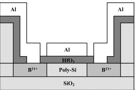
2.1 Device Fabrication
As shown in the Fig 2.1, the fabrication of the device was started by depositing a 50nm-thick un-doped amorphous Si (a-Si) layer at 550℃ by low pressure chemical vapor deposition (LPCVD) on the Silicon substrate which was capped with a 500nm-thick thermal oxide layer. Then the a-Si layer was re-crystallized to poly-silicon channel film by the SPC process at 600℃ for 24hr in a N2 ambient. The source and the drain regions were implanted with boron for
p-channel TFTs (15keV at 5x1015cm-2). Then the S/D regions were activated at 600℃ for 24hr annealing in a N2 ambient. After the implantation of S/D regions,
a 500nm-thick TEOS oxide was deposited on the poly-Si channel film at 700℃ by the LPCVD system for the device isolation. Then the TEOS oxide film was patterned and then etched to be the field oxide for the active region formation. For the HfO2-TFTs, the 175Å, 415Å and 745Å-thick HfO2 filmswere deposited
by the electron-beam evaporator system at room temperature and the process pressure of 10-5 torr. Then all the samples were annealed in the horizontal furnace with O2 at 400℃ for 0.5hr to improve the quality of the gate dielectrics.
After the patterning of the contact holes, aluminum (Al) was deposited by the electron-beam system at room temperature and 5x10⁻⁷base pressure as the gate electrodes and the S/D contact pads. Finally, the TFT devices were finished by the definition of source, drain and gate contact pads. All the fabrication
processes were shown in the Fig. 2.1.
2.2 Measurement
The NBTI tests are performed on 10µmx10µm p-channel TFTs with HfO2
thickness of 175, 415 and 745Å, with source and drain grounded during the stress. The samples are stress at a constant voltage for 1000 seconds. The threshold voltage (VTH) and the transconductance (Gm) are extracted using Id-Vg
sweeps performed during periodic interruptions of the stress. Measurements are performed at various stress voltages and 2 different temperature – Room temperature (RT) and 125°C.
2.3 Method of Parameter Extraction (Determination of
Thresholod Voltage)
Threshold voltage Vth is one of the most important electrical parameter of
semiconductor. However, the precise threshold voltage of the device is difficult to define. Therefore, several methods have been proposed to extract the Vth of
different kinds of devices. In MOSFETs, there are two common methods for the determination of Vth. One of them is the linear extrapolation method with the
drain current measured at a drain voltage of 50~100mV to make sure the operation in the linear regime. According to the ideal Id-Vg relation in the linear
) )]( ( 2 1 ) [( ( GS th DS D SD DS D SD ox eff d V V V I R V I R L W C I − − − − =µ ……… …….(2.1) ) ]( 2 1 [ GS th DS DS ox eff V V V V L W C − − ≅ µ ……… ……….(2.2)
It is worthy to note that the equation (2.2) is only valid as the series resistance is negligible such as source and drain resistance RSD, which usually
can be ignored at a low drain current and low drain bias. It is a common practice to find the point of the maximum slope of the Id-Vg curve (Gm_max) and fit a
straight line to Id=0 from this point. According to the equation (2.2), we can
obtain a VG point which is corresponding to Id=0. Hence, the Vth defined by the
extrapolation method is : 2 DS GS th V V V = − ………(2.3)
In this work, Vth is defined by the other method which is different from the
above description. We make use of a more simple way which is called constant drain current method. This method is utilized in almost every paper in the TFT field. The Vth derived by this way is close to the Vth obtained from the
extrapolation method. Here, the Vth is defined as the point at
VDS=∣0.1V∣where the drain current Id=(W/L)*100nA for n and p channel,
where the W and L are the channel width and the channel length respectively. In this paper, devices were all measured in the size of W=10µm and L=10µm. Thus the Vth is defined as the gate voltage where the drain current Id=1*10
-7
A in all of our discussions.
2.3.1 Determination of subthreshold swing
Subthreshold slope (S.S.) is a typical parameter to describe the gate control ability, which reflects how fast the device can be switched from off state to on state. It is defined by the amount of the gate voltage needed to increase or decrease the drain current by one order of magnitude. The S.S should be independent of gate voltage and drain voltage. However, the S.S. of a device is usually affected by the various degradation effects such as charge sharing, avalanche multiplication and punchthrough effect. The S.S. is usually related to the undesirable and inevitable phenomenon such as series resistance and interface states. In LTPS TFTs, the S.S. is also dependent on the trap state in the grain boundaries. It has been reported that the the S.S is strongly related to the trap states near the mid-gap (deep energy level), which is originated from the dangling bonds [1], besides, the low temperature process of the LTPS-TFTs will result in a poor interface between the gate dielectrics and the channel films. Briefly speaking, the bulk trap states and interface states will degrade the S.S. of LTPS-TFTs.
The formula of subthreshold slope was defined as :
1 ] ) ( ) (log [ . . − ∂ ∂ = GS DS V I S S ………… …………..(2.4)
2.3.2 Determination of on/off current ratio
On/off drain current ratio is other important parameters of TFT devices. High On/off ratio reflects not only the high on current but a small off current (or
leakage current). In TFTs, the on/off drain current ratio of six orders is required for the applications of AMLCDs.
In this paper, the on current is defined as the point at a fixed drain bias of 0.1V where the drain current is at a maximum of the Id-Vg curve. The off current
is defined as the point at a fixed drain bias of 0.1V where the drain current is at a minimum. Therefore, the on/off drain current ratio can be derived by the following formula: V V d d off on d
I
I
I
I
1 . 0 min _ max _ ==
………(2.5)2.3.3 Determination of field effect mobility
The field effect mobility (µFE) is usually determined from the maximum
value of transconductance (Gm) at a low drain bias. The drain current in the
linear region (VDS < VGS-Vth ) can be approximated as the following equations :
− − = 2 2 1 ) ( ) ( GS th DS DS ox FE DS V V V V L W C I µ ………. ………(2.6)
where W and L are the channel width and the channel length, respectively;Cox is
the gate oxide capacitance per unit area and Vth is the threshold voltage. Thus,
the transconductance is given by the differential equation:
DS ox FE GS DS m V L W C V I G =µ ( ) ∂ ∂ = ………. ……….(2.7)
Therefore, the field-effect mobility is defined as follows: 0 max _ ) ( → = DS V DS ox m FE V L W C G µ ………(2.8)
2.3.4 Determination of the trap state density
In LTPS-TFTs, the trap state density (Nt), which originates from dangling
bonds or strained bonds located in the grain boundaries of poly-Si films. The trap state in the channel region will trap free carriers and result in potential barrier height VB to degrade the carrier transportation like the degradation of the
field-effect mobility ( μFE), higher threshold voltage (Vth), subthreshold swing (S.S.) and leakage current. Therefore, the grain boundary trap state density is an important parameter that affects the electrical transport properties significantly of poly-Si films. Therefore, it is necessary to extract the trap state density in the channel film. Many researchers have investigated the electrical characteristics and the carrier transport mechanism in the poly-Si TFTs. Among the lots of grain boundary trap state-extraction method, The trap state density is usually derived by the Lenvinson and Proano method [2][3]. And the method is described as follows:
By modifying the mobility µb and replacing the dopant concentration with gate
induced charge density NG, the corrected expression of the transfer
characteristics (ID-VG) at low drain voltage in the poly-Si films is very similar
with that in the regular MOSFET’s. It is expressed as:
) ) ( 8 exp( ) )( ( 2 3 0 th G ox s ch t D th G ox D V V C kT t N q V V V L W C I − − − = ε µ ………..(2.9)
The equation above was modified by Proano et al [3]. It is found that the behavior of the carrier mobility under low gate bias can be expressed more accurately by using the flat-band voltage VFB instead of the threshold voltage
(Vth). The flat-band voltage VFB is defined as the gate voltage which corresponds
to the minimum drain current. Furthermore, Lenvinson et al. [2] assumed that the channel thickness tch is constant and equal to the thickness of the poly-Si
film tpoly-Si. This simplified assumption is acceptable only for the very thin film
(tpoly-Si), which is not applicable to the common thickness for the poly-Si TFTs.
As a result, a better approximation for the channel thickness tch in an undoped
poly-Si film is given by defining the channel thickness as the thickness at which 80% of the total charge resides. Therefore, by solving the Poisson’ equation, the channel thickness is given by the equation:
) ( 8 FB G ox ox s ch V V qC kT t − = ε ε ……….……..(2.10)
Substituting the modified terms discussed above for the equation (2.9), thus the drain current ID can be expressed as the following equation:
) ) ) ( exp( ) )( ( 2 2 2 2 0 FB G ox s ox t D FB G ox D V V C N q V V V L W C I − − − = ε ε µ ………(2.11)
According to the equation (2.11), we can extract the trap state density (Nt) from
the slope of the curve ln[ID/(VG-VFB)]versus (VG-VFB) -2
. the effective grain boundary trap state density Nt can be determined from the square root of the
slope described as follows:
slope q
C
N ox
SiO2
a-Si
(a) Thermal oxidation and an amorphous Si (α-Si) film was deposited by LPCVD.
SiO2
Poly-Si
(b) The α-Si film was crystallized into the poly-Si film by SPC at 600℃ for 24hr.
SiO2
Poly-Si
B11+ B11+
(c) The source and drain regions (S/D) were implanted with boron and then activated at 600℃ for 24hr.
SiO2
Poly-Si
B11+ B11+
(d) TEOS SiO2 was deposited as the field oxide and the active region was
SiO2
Poly-Si HfO2
B11+ B11+
(e) The HfO2 films with the thickness of 175Å, 415Å and 745Å were
deposited by the e-beam evaporator as the gate dielectrics. Post deposition anneal (PDA) was performed at 400℃ in the O2 ambient for
the densifying of the HfO2 films.
SiO2
Poly-Si HfO2
B11+ B11+
SiO2 Poly-Si HfO2 B11+ B11+ Al Al Al
(g) Aluminum films were deposition by the e-beam evaporator as gate electrodes and the gate and S/D regions were defined and opened.
SiO2 Poly-Si HfO2 B11+ B11+ Al Al Al
(h) The HfO2-TFT Devices are sintered at 400℃ for 30 min in a N2
ambient.
Chapter 2
Reference
[1] I-W. Wu, Y-Y. Huang, W. B. Jackson, A. G. Lewis, and A. C. Chiang, “ Passivation kinetics of two types of defects in polysilicon TFT by plasma hydrogenation,” IEEE Electron Device Lett, vol. 12, pp. 181-183, 1991.
[2] J. Levinson, F. R. Shepherd, P. J. Scanlon, W. D. Westwood, G. Este, and M. Rider, “ Conductivity behavior in polycrystalline semiconductor thin film transistors,” J. Appl. Phys, vol. 53, pp.1193-1202, 1982.
[3] R. E. Proano, R. S. Misage, D. G. Ast, “Development and electrical properties of undoped polycrystalline silicon thin-film transistors,” IEEE Trans. Electron Devices, vol. 36, pp. 1915-1922, 1989.
Chapter 3
Electrical Characteristics of the p-channel LTPs TFTs with
Different Thickness of High-κ Gate Dielectrics
3.1 Electrical Characteristics
In this work, several possible mechanisms that contribute to the degradation or the enhancement of the peak transconductance (Gm_max) are systematically
investigated and a new model is firstly proposed to explain the enhanced Gm_max
for the TFTs with the thicker HfO2 gate dielectrics.
Fig. 3.1 (a) shows the transfer characteristics (ID-VG) of the poly-Si TFTs
with HfO2 gate dielectrics, which had physical thickness of 250, 500, 700, 1000
and 1700Å, respectively. It is surprisingly that the value of the peak transconductance (Gm_max) increases with the thickness of the HfO2 layer. To
further confirm this phenomenon, we have measured and extraccted five values of Gm_max and calculated the average of them of each sample with different HfO2
thickness as shown in the Fig. 3.1 (b). We found that the same trend is observed clearly. Considering the instability of the fabrication process, this phenomenon may be due to some errors in the fabrication process. Thus, to make sure the repeatability of this phenomenon, we performed the second run of the poly-silicon TFTs with different thickness of the HfO2 layers, which had
physical thickness of 175, 415 and 745Å, respectively. The transfer characteristics (ID-VG) of the poly-Si TFTs with 175Å to 745Å-thick HfO2 gate
respectively. As shown in the Fig. 3.2 (a), the Gm_max of the 175Å and the 415Å
sample (TFTs with 175Å, 415Å and 745Å-thick HfO2 layer are called 175Å,
415Å and 745Å sample for short thereafter in this paper) are nearly the same but are much smaller than that of the 745Å sample before sintering, whereas the value of Gm_max increases with the HfO2 thickness after sintering of TFT devices
at 400℃ for 30 minutes in a N2 ambient. To further confirm this phenomenon,
we also measured and extracted five values of Gm_max of each device with
different thickness of HfO2 and calculated the average of them. We found that
the same trend is also shown in the Fig. 3.2 (c). The Figure 3.2 (d) shows the Gm_max dependence of temperature. We found that the Gm_max still increases with
the HfO2 thickness even at high temperature of 100℃ and therefore we can rule
out the contribution of the remote phonon scattering that degrades the field effect mobility of the TFTs with the thin HfO2 layer. The measured as well as the
extracted device parameters before and after sintering are summarized in the Table 2.1 (a) and (b). It is proved that the phenomenon that the Gm_max increases
with the HfO2 thickness is repeatable. As far as we know, the field effect
mobility (µFE) is proportional to the value of the Gm_max versus the gate
capacitance density (Cox). What’s more, the gate capacitance density is inversely
proportional to the thickness of the gate dielectrics, that is to say, a smaller gate capacitance density will be obtained for a thicker gate dielectric film. As a result, it is suggested that the field effect mobility increases with the thickness of the HfO2 layer more significantly if the Gm_max is divided by the gate capacitance.
Based on the knowledge we had before, the grain boundary potential barrier height in the channel region is reduced with the increasing free carrier density during the strong inversion. Because the larger gate capacitance will result in the