國 立 交 通 大 學
電子物理學系
碩 士 論 文
利用接觸蝕刻停止層以及下凹式源極和汲極
對電晶體載子遷移率提升之研究
A Study of Mobility Enhancement by
Contact Etch Stop Layer and Recess Source/Drain
研 究 生 :穆政昌
指導教授 :趙天生 博士
利用接觸蝕刻停止層以及下凹式源極和汲極
對電晶體載子遷移率提升之研究
A Study of Mobility Enhancement by
Contact Etch Stop Layer and Recess Source/Drain
研 究 生 : 穆政昌 Student : Zheng-Chang Mu
指導教授 : 趙天生 博士 Advisor : Dr. Tien-Sheng Chao
國立交通大學
電子物理學系
碩士論文
A Thesis Submitted to Department of Electrophysics
National Chiao Tung University
in Partial Fulfillment of the Requirements for the Degree of
Master of Science in Electrophysics
July 2010
Hsinchu, Taiwan, Republic of China.
中華民國 九十九 年 七 月
利用接觸蝕刻停止層以及下凹式源極和汲極
對電晶體載子遷移率提升之研究
研 究 生 : 穆政昌 指導教授 : 趙天生 博士 國立交通大學 電子物理學系 摘要 在本論文中,我們將 n 型電晶體製作於(110)的基板上,加上接觸蝕刻停止 層以及下凹式源極和汲極的結構,來提升通道的應力,進而改善載子遷移率。 其 中,我們的元件活化是使用微波退火方式活化離子佈值。 另外,我們從材料分 析中發現,氮化矽(接觸蝕刻停止層)材料經過微波退火過程之後,會提高伸張應 力, 所以我們將此項方法加入製程之中,來提升接觸蝕刻停止層的伸張應力, 可以有更高的載子遷移率。 之後,我們再對電晶體做熱載子測試,針對元件的 可靠度做一簡單的分析。 在實驗結果中,我們發現接觸蝕刻停止層經由微波活化提升伸張應力可以明 顯改善驅動電流。而在閘極線寬縮小至 0.2 微米以後,下凹式源極和汲極的結構 加上微波活化提升伸張應力,可以提高驅動電流。而在氮化矽沉積的過程之中, 因沉積氧化矽的反應氣體含有大量的氫元素,氫元素在沉積過程中擴散進入通道, 修補矽與氧化矽交界的懸浮鍵,因而降低了表面陷阱密度。在熱載子分析部分, 熱載子對元件介面的破壞對於下凹式源極和汲極的結構是相當嚴重的。因為在測 試過程中,熱載子會被捕捉在閘極與 spacer 之中,造成在做完熱載子測試後的驅 動電流量測中,電子經過有大量電子被捕捉的閘極與 spacer 附近,會產生散射, 而我們會發現驅動電流有明顯的衰減。並且在等效電壓變動(threshold voltageshift)對熱載子測試時間的結果之中,下凹式源極和汲極的結構的等效電壓明顯 的變動也證明此項結果。
A Study of Mobility Enhancement by
Contact Etch Stop Layer and Recess Source/Drain
Student:Zheng-Chang Mu Advisors:Dr. Tien-Sheng Chao
Department of Electrophysics National Chiao Tung University
Abstract
In this thesis, we fabricate nMOSFET with recess source/drain and CESL (contact etch stop layer) on (110) substrate for channel strain and carrier mobility enhancement. Dopant activation is executed by the microwave anneal. Besides, from the result of material analysis, SiN film annealed by microwave shows with a tensile stress shift. This technique is used in device fabrication for tensile strain and mobility enhancement.
From the result, CESL with microwave anneal for tensile enhancement technique improves driving current obviously. As gate length scales down to 0.2μm, recess source/drain structure with CESL with microwave anneal for tensile enhancement technique significantly enhances driving current. During SiN deposition, hydrogen diffuses to the interface of silicon and oxide to passivate dangling bonds. From charge pumping measurement, interface state density of SiN split is smaller than that of control split.
From hot carrier stress analyses, the recess source/drain device shows a serious degradation after the hot carrier stress. In the process, channel hot electron would be trapped in the spacer. When the electrons flow through the spacer, Coulomb scattering
would become serious in current-voltage measurement. As a result, current-voltage curves show a serious degradation. This phenomenon is confirmed from the result of shift of threshold voltage versus time under stress.
誌 謝
兩年的碩士生活轉眼間就過去了,在這段期間很辛苦,但也很充實。而能夠 把這篇論文順利的完成,首先要感謝我的指導教授趙天生老師,有您的鼓勵及關 心才讓我有動力及信心將這篇論文完成。接下來要感謝李耀仁博士,在實驗上或 是想法上給予的協助,以及在製程上的訓練都對我有莫大的貢獻。再來要感謝呂 侑倫學長在製程上的協助,及對於我所有問題很有耐心的解惑。 要特別感謝廖家駿學長及林岷臻學姊對於實驗上及問題上的建議及王冠迪 學長在量測上的大力協助,對於本論文的完成貢獻良多。 由衷感謝郭柏儀、江宗育、呂宜憲、林哲緯、吳翊鴻、嚴立丞、林威良、蔡 博安、王智盟、高國興、張競之、鄭子彥、林玉喬、黃士安、葉啟瑞、楊才民等 學長姐在實驗室生活上或是課業上的關心及照顧。一起打拚的同學黃國欽、莊尚 勳、薛富國、林婉琪、劉聿民、李時璟及可愛的學弟妹吳立盈、陳昱璇、謝其儒、 薛芳昌、張添舜,感謝你們平常帶給實驗室的歡樂,讓實驗室一直都是這麼有趣。 國家奈米元件實驗室的工程師周棟煥、劉正財、巫振榮、謝錦龍、鍾昌貴、 彭馨誼、吳鴻佑、侯福居,代工小姐魏耘木疌、周家如、林婉貞、范庭瑋、陳琇 芝、趙子綾、蕭明娟、徐台鳳,在製程中的所有幫忙我都由衷感謝。 最後,要感謝我的母親,練菊枝女士,因為有您的支持,才有我現在的成就。 穆政昌 誌于風城交大 2010/07Contents
Chinese Abstract……….………i
English Abstract……….iii
Acknowledgements………v
Table Captions……….………...…...viii
Figure Captions………....ix
Chapter 1 Introduction………..…………...………1
1-1 General Background………..………...…..1
1-1.1 Strain Technology………..…………....….1
1-1.2 Orientation and Ideal CMOSFET….……….………..……..4
1-2 Motivation……….………...………..5
1-2.1 Recess Source/Drain Technique…….………5
1-2.2 Low Temperature Microwave Anneal………..……..5
1-2.3 Low Temperature Anneal for Strain Enhancement………...6
1-2.4 The Combination of Recess Source/Drain Technique and
Microwave Anneal ………..……...………6
Chapter 2 Material Analysis, Device Fabrication, and
Measurement………...…...……….………8
2-2 Device Fabrication………..………..……8
2-3 Measurement…….……….……….…..9
Chapter 3 Result and Conclusion……….….11
3-1 Material Characteristic……….…..…11
3-2 Device Characteristic………..12
3-2.1 Basic Device Analysis………...…..12
3-2.2 Capacitor-Voltage and Current-Voltage Characteristics..….12
3-2.3 Interface State………..….14
3-2.4 Series Resistance……….…….15
3-2.5 The Device Characteristics After Hot Carrier Stress
Process……….….16
Chapter 4 Summary and Conclusion……….18
References………....20
Table Captions
Chapter 1
Table.1-1 The stress types for FET enhancement on general <110>/(100)
substrate……….……….31
Chapter 2
Figure Captions
Chapter 1
Fig. 1-1 The transistors count of CPU increases with year, and doubles every 2 years………...………..25
Fig. 1-2 Transistor size scale down for high speed and high density CPU………...25
Fig. 1-3 ITRS 2009 Process Integration Device and Structures Logic Potential
Solution………26
Fig. 1-4 Electron mobility decrease with gate length………26
Fig. 1-5 The conduction band valley in k space with and without biaxial tensile strain.(The energy band diagram of electron split for biaxial tensile strain.)………...27
Fig. 1-6 The valance band in k space with and without biaxial tensile strain……...28
Fig. 1-7 (a) Strain silicon technique to enhance electron mobility……….…..……29
(b) Raised source and drain to enhance hole mobility……….……29
Fig. 1-8 Strain silicon and raise source/drain technique for nMOS and pMOS
enhancement……….………30 Fig. 1-9 The CMOS performance for strain enhancement structure……….………31 Fig. 1-10 Channel direction on three type of orientation substrate………...32
Fig. 1-11 The carrier mobility for different channel direction on different orientation
Fig. 1-12 Two types of Hybrid-Orientation Technology (HOT) substrates………..33
Fig.1-13 Symmetrical current versus voltage characteristics for HOT substrates…33
Fig. 1-14 TEM cross section of FET with recess Source/Drain about 20nm………34
Fig. 1-15 The Ion − Ioff performance for NFET and PFET by recess S/D……...…34 Fig. 1-16 The SIMS profile of boron that before and after RTA and microwave annealing. ……….….35
Fig. 1-17 The stress shift by RTA anneal for different composition of SiN….…..35
Fig. 1-18 The model of stress shift after thermal annealing……….…….36 Fig.1-19 The intrinsic and microwave annealed stress of SiN 200nm……...…….36
Chapter 2
Fig. 2-1 Strain measurement system for measuring the radius of curvature……….37
Fig. 2-2 Process flow for device fabrication……….37
Fig. 2-3 (a) Standard LOCOS isolation process………39
(b) Gate oxide growth, poly silicon deposition, and hard mask deposition.39
(c) E-beam lithography process………39
(d) Dry etching of gate formation, and photo resist remove………40
(e) Source/Drain extension implant with As (Dose: 1 × 1015cm−2, Energy: 10KeV)……….…..40
(g) Dry etching to define the recess source and drain………..41
(h) Source/drain implant with P (Dose: 5 × 1015cm−2, Energy: 10KeV)...41
(i) First microwave annealing to activate doping……….41
(j) PECVD tensile SiN deposition………42
(k) Second microwave annealing to enhance the SiN stress………42
(l) PECVD TEOS passivation deposition………42
(m) Dry etching to define the contact hole, metal deposition by PVD, and dry etching to define the metal pad……….………...43
Fig. 2-4 Four-point probe measurement to extract sheet resistance………..44
Fig. 2-5 Charge pumping measurement setup. (Fixed gate voltage amplitude mode.)………...44
Fig. 2-6 Hot carrier stress to induce hot electron traps………..45
Chapter 3
Fig.3-1 Strain for intrinsic, anneal, and strain shift value with different nitride thickness………...46Fig.3-2 Nitride stress for different thickness……….…….46
Fig. 3-3 Temperature profiles for microwave and RTA anneal conditions………47
Fig.3-4 The SiN stress shift after microwave and RTA process………47
Fig.3-5 The TEM cross section of control sample...……….48
CESL 2000A , sample. The Recess depth is about 30nm……….49
Fig. 3-7 Temperature versus time of microwave annealing for device activation. (2800W,600s)………..………50
Fig. 3-8 Sheet resistance for poly gate and source/drain region………...50
Fig. 3-9 The capacitance for W/L=20/20(um) and frequency at 100KHz.
The effective oxide thickness=2.98nm in the inversion region…………..51
Fig. 3-10 The ID − VG performance for W/L=10μm/10μm nMOS………51 Fig. 3-11 The ID − VG performance for W/L=10μm/0.4μm nMOS………..52 Fig. 3-12 The ID − VG performance for W/L=10μm/0.2μm nMOS………..52 Fig. 3-13 The characteristic of transconductance maximum and gate length……...53
Fig.3-14 The recess source/drain characteristic for transconductance versus gate
voltage for high gate electric field……….53
Fig. 3-15 (a) Electron path from source to drain for normal MOSFET………54
(b) Electron path from source to drain for recess S/D MOSFET………...54
Fig. 3-16 Subthreshold swing of nMOSFET for all split with W/L=10μm /0.2μm..55
Fig. 3-17 Drain induce barrier lowing characteristics for nMOS………...55
Fig. 3-18 The charge pumping current of nMOS on <100>/(110) . The W/L=10μm /0.4μm, pulse frequency is 10MHz, and amplitude is 1.5V……….56
Fig. 3-19 The charge pumping current of nMOS on <100>/(110) . The W/L=10μm /0.2μm, pulse frequency is 10MHz, and amplitude is 1.5V………56
Fig. 3-20 Hydrogen diffuse to the interface and passivate the dangling bond in
deposit SiN process………..…..57
Fig. 3-21 The schematic a MOSFET with source and drain resistances…….…….57
Fig. 3-22 Rtotal versus 1/(VG− Vth) for difference channel length…………..……58 F i g . 3 - 2 3 RSD i s t h e l i n e i n t e r c e p t a t m = 0 , C E S L 1 = 2 11 6 . 5 ( Ω ) ,
Recess 2=2059.2(Ω)...58
Fig. 3-24 Impact ionization induce substrate current at VG = 5V………59 Fig. 3-25 Subthreshold and transconductance characteristics after 5000s hot carrier
stress for control sample………59
Fig. 3-26 Subthreshold and transconductance characteristics after 5000s hot carrier
stress for CESL 1 sample………..60
Fig. 3-27 Subthreshold and transconductance characteristics after 5000s hot carrier
stress for Recess 2 sample………60
Fig. 3-28 (a) The electron trap in spacer at the process of hot carrier stress…….61
(b) The electron traps induce Coulomb scattering at current-voltage
measurement. ………61
Fig. 3-29 Threshold voltage shift with hot carrier stress time………..62
Fig. 3-30 Transconductance degrade with stress time for Control, CESL 1, and
Chapter 1
Introduction
1-1 General Background
Field Effect Transistor (FET) is used in advanced integrated circuit (IC) products. One of representative product for advanced semiconductor is computer. To enhance the speed and advance the compute efficiency of computer, the transistors count of CPU increases with year is shown in Fig. 1-1[1]. To increasing the transistors count of CPU, transistors must be scaled down. Fig. 1-2 [2] shows the transistor scale down 30% for every generation. The goals of MOSFET scale down are higher transistor density and high operating speed for CPU.
From International Technology Roadmap for Semiconductors (ITRS) 2009 [3], the FET physical gate length scale down to 29nm for high-performance logic beyond 2009. Fig. 1-3 show the process integration device and structures logic potential solution.
1-1.1
Strain Technology
As FET scale down, short channel effect and surface roughness would become the main issue for nanometer-scale transistors. In Fig. 1-4[4], the mobility degraded by surface roughness scattering obviously as the gate length under 100 nm. To enhance the carrier mobility which degraded by surface roughness scattering, strain technique was introduced in FET fabrications.
in integrated circuits. The mobility associate with the effective carrier mass m∗ from μ = mqτ∗ ⋯ eq. (1 − 1)
, where μ is carrier mobility and τ is the mean free time of carrier. The effective carrier mass associate with the band diagram in reciprocal (k) space, from
m∗ = ℏ �d2E
dk2� ⋯ eq. (1 − 2)
, where ℏ is Plank constant divided by 2π and E is the energy in k space. We could derive the effective mass from the energy band diagram in k space.
Biaxial tensile strain is a general method to enhance electron mobility [5-7]. Si channel grown on a relaxed SiGe substrate as shown in Fig. 1-8(a), the Si crystal would be biaxial-tensile strained by SiGe substrate. Fig. 1-5(a) shows the conduction band valley in the reciprocal space. For electrons, the biaxial tensile strain caused the degenerate band valleys splitting. Two fold valleys with lower energy and four fold valleys with higher energy are shown in Fig. 1-5(c). The electron population shift to two fold out-of-plane valleys in the reciprocal (k) space as shown in Fig. 1-5(b). The total electron effective mass is given by
m∗= � 1 6 � 2 ml� + � 4 mt�� −1 … eq. (1 − 3).
The longitudinal mass (parallel to the axis) is given by ml=0.98m0 (m0 is free electron mass), the transverse mass (perpendicular to the axis) is given by mt =0.19m0. Most electrons populate at two fold valleys, which result more electrons with an in-plane transverse mass (0.19m0) and less electrons with out-of-plane longitudinal mass (0.98m0).The direction from source to drain is transverse direction, most of electron with transverse mass (0.19m0). Then the electron mobility is
enhanced by biaxial tensile stress. From reference [8] as shown in Fig. 1-7(a), the universal curve was the line which linked the peak mobilities of bulk Si for nFETs, and the strained Si technique could enhance effective electron mobility obviously. From the viewpoint of holes, the biaxial tensile strain split the valence bands for light hole band and heavy hole band as shown in Fig. 1-6(d). The heavy hole band is low energy and the light hole band is high energy. Most of hole populated at light hole band. From source to drain, holes transport for in- plane direction, the energy band in k space as shown in Fig. 1-6(b). From Eq. (1-2), the effective mass of hole at light holes band is heavier than heavy hole band in the situation, so the effective mass of hole become heavier for in-plane transportation. This is why pFET degraded by tensile stress.
To enhance the holes mobility for pFET, reference [9] proposed that epitaxial SiGe form on recess source and drain regions, as shown in Fig. 1-8(b), to enhance hole mobility. The direction from source to drain is out-of-plane direction, most of hole populate at light hole band as shown in Fig. 1-6(d). In Fig. 1-6(c), the E-K diagram for out-of-plane valence band, the light hole band curve is smaller than the heavy hole band. In this situation, from Eq. (1-2), the effective mass for most of hole is become smaller. Then hole mobility would be enhance in pFET as shown in Fig.1-7(b).
Besides, SiN film with stress deposited on transistors could strain the channel. SiN cap on transistors with tensile/compressive stress would enhance the electron/hole mobility [10-12]. It is well-known process strain technique in advanced CMOS fabrication. Recently, SMT (stress memorization technique) was used for enhancing nFET performance [13]. The mechanics of SMT is using the high temperature anneal to enhance the tensile stress of SiN, and channel strained by the
stress shift of SiN [14-15].
The direction of strain would affect the MOSFET characteristics. Table 1-1 [16-17] summarizes the stress effect CMOS performance on general channel direction <110> and substrate orientation (100). For nFET, the x and y direction with tensile strain and z direction with compressive strain would enhance electron mobility. For pFET, the y and z direction with tensile strain and x direction with compressive strain would enhance hole mobility.
1-1.2
Orientation and Ideal CMOSFET
Fig. 1-10 shows the different channel directions on (100), (110), (111) substrate orientations [18], it’s also a factor for effecting on carrier mobility. From Fig. 1-11 [19-20] (a) and (b), we could summary the effect on different channel directions with (100), (110) and (111) substrate orientations. NFETs fabricate on <110> channel direction and (100) substrate orientation with high electron mobility. PFETs fabricate on <110> channel direction and (110) substrate orientation with high hole mobility.
As a result of Fig. 1-11, Hybrid-Orientation Technology (HOT)[19] combined the nMOS with (100) channel and pMOS with (110) channel for high carrier mobility as shown in Fig. 1-12. HOT structure also proposed for ideal CMOS which with symmetrical current -voltage characteristics as shown in Fig. 1-13. But it more cost with the additional processes is the disadvantage for HOT structure. Ideal CMOS could fabricate by other low cost methods.
One method of ideal CMOS is fabricating CMOS on (100) substrate, and enhancing the pMOS performance. In 2006, X. Chen et al [21] proposed Stress Proximity Technique to improve the pMOS performance on (100) substrate. NMOS fabricate on (100) substrate with high electron mobility, and we could only enhance
the pMOSFET performance on (100) substrate for ideal CMOS.
The other method for ideal CMOS is fabricating CMOS on (110) substrate, and enhancing the nMOSFET performance. PMOS with high intrinsic hole mobility on (110) substrate, we could only enhance the nMOSFET on (110) substrate for ideal CMOS. And this thesis is study of enhancing the nMOSFET performance on (110) substrate.
1-2 Motivation
1-2.1 Recess Source/Drain Technique
From the reference [22], VLSI technology 2008, S. S. Tan et al proposed recess
Source/Drain technique to enhance channel strain. Fig 1-14 shows the TEM cross section of the recess S/D structure, and all FETs are on <110> channel direction and (100) substrate orientation. Fig 1-15 shows the Ion − Ioff performance of NFET and PFET. Recess S/D structure enhance the on current of PFET about 15%~40%, but not for NFET.
But the performance of recess S/D NFET structure on (110) substrate is unknown. Maybe we could fabricate NFETs on (110) substrate with enhancement by recess S/D technique. It might be a method to improve the electron mobility on (110) substrate, and then we could realized the ideal CMOS on (110) substrate.
1-2.2 Low Temperature Microwave Anneal
Ion implantation is the standard process for CMOS fabrication. After implantation, CMOS would anneal for doping activation. Because of the CMOS scale
down, anti-punch through implantation is introduced to avoid the punch through effect. But the main factor of increasing dopant diffusion is the thermal budget of device fabrication [23]. Therefore, decrease the thermal budget should be the key point of device scaling down.
The dopant activation has been used in the fabrication of thin film transistor (TFT) [25]. It is different that anneal mechanism of RTA and microwave. The thermal source heat the surface of the wafer, and the heat transmit to the inside of the wafer to activate dopant for RTA. And the microwave run through the wafer, the particles accept the energy of the microwave to oscillate and anneal the dopant.
In Fig. 1-16 [25], the SIMS profile shows the boron diffusion after RTA 900˚C 15s and Microwave 100s. After 100 seconds microwave anneal is almost the same as implanted. The dopant diffusion is effectively suppressed by microwave anneal [26].
1-2.3 Low Temperature Anneal for Strain Enhancement
From reference [14], the stress of SiN is associate with the anneal temperature. And reference [15] proposed that the stress shift with difference composition of SiN by rapid thermal anneal. Fig 1-17 [15] shows the stress of SiN for intrinsic, annealed, and stress shift. The SiN films are different composition of Si and N. The SiN strain with about 1200MPa after annealed for SiH4 high sample. Fig 1-18 [15] shows the model that stress shift enhancement for thermal anneal. As annealed, the SiN expanded by thermal mechanism. But high temperature would effect upon the implant profile.
From reference [14-15], we have an idea of strain enhancement by microwave annealing. We check the microwave enhance stress ability, and measuring the stress
before and after microwave annealing. In Fig. 1-19, the intrinsic stress is about 350MPa as we deposited SiN 200nm on wafer. Then we anneal the wafer by microwave 2100W 600s, the after annealed stress is about 1250MPa. It indicates microwave annealing could enhance tensile stress as RTA.
1-2.4 The Combination of Recess Source/Drain Technique and
Microwave Anneal
We want to combine recess source/drain technique and microwave annealing to enhance nitride stress for our device fabrication. It might enhance channel strain and electron mobility of nMOSFET on (110) substrate.
Chapter 2
Material Analysis, Device Fabrication, and
Measurement
2-1 Material Analysis
We discussed the strain of nitride for intrinsic and annealed condition. Our
deposition of SiN on 6-in silicon wafers by Oxford PECVD in 850 mTorr with high frequency RF power 20 Watt and the temperature is 300°C. The recipes for SiN deposition were SiH4 for 20 sccm, NH3 for 20 sccm, and N2 for 980 sccm. The nitride strain was measured by stress measurement system [27]. Fig. 2-1 show strain measured by the shift of curvature.
First, we studied the relation of nitride thickness and strain. We deposited the SiN 20nm~200nm on wafers by PECVD and strain measurement for intrinsic strain. After deposition, the wafers annealed by microwave (2100W, 600s) and RTA (900˚ C,15s). We measured the stain enhancement by annealed process for different thickness condition of nitride.
Then, we compared the relation of strain and annealed condition. All the wafer was deposited SiN 200nm and compared the strain shift. Wafers annealed by microwave (2100W, 600s), RTA (500˚C, 600s), and RTA(900˚C, 15s) . After annealing, strain measurement for different annealed condition.
2-2
Device Fabrication
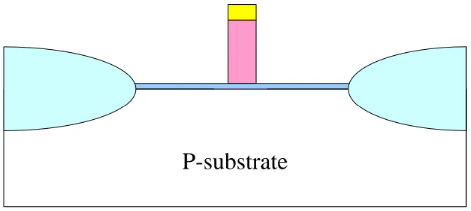
Fig. 2-2 show the process flow of device fabrication, and Figs. 2-3(a) ~ (m) are the steps of process. NMOSFET fabricated on 6-in p-type (110) silicon wafers. First,
well implanted BF2 with the dose and energy were 1.2 × 1013cm−2 and 70 KeV. Then standard LOCOS for isolation. Threshold voltage implant BF2 with the dose and energy were 1 × 1013cm−2 and 90 KeV. Anti punch through implant Boron with the dose and energy were 2 × 1012cm−2 and 70 KeV.
Gate oxide was grown in vertical furnace, and the thickness were 3nm for (110)
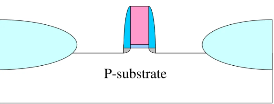
orientation wafers. In situ phosphorous poly gate 100nm was deposited by vertical furnace; gate was patterned by e-beam lithography and dry etching. After halo and S/D extension implantation, low temperature PECVD TEOS deposited and spacer was formatted by dry etching.
After spacer formation, S/D recessed by dry etching for recess S/D splits. S/D implant phosphorous with dose and energy were 5 × 1015cm−2 and 10 KeV. After body etching, body implanted BF2 (5 × 1015cm2, 40 KeV) for ohmic contact.
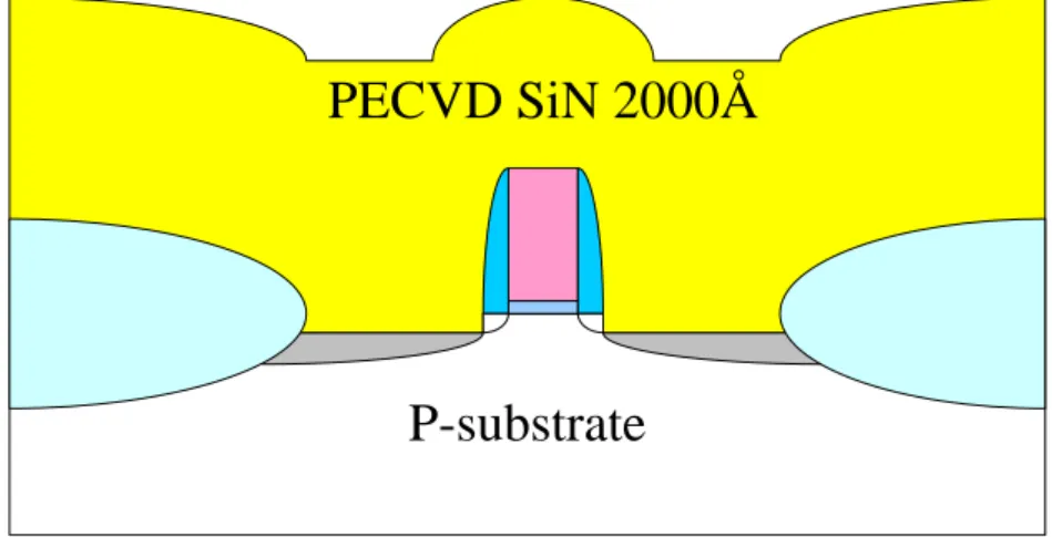
First microwave anneal (2800W, 600s) the implant activation. After deposition of PECVD SiN 200nm (control sample without SiN deposition), we used second microwave annealing for SiN tensile strain. Finally, 300nm TEOS oxide passivation was deposited by PECVD. Contact etching process by dry etching, metal contact deposited by PVD, and metal pad etching by dry etching.
2-3
Measurement
Basic current-voltage (I-V) and capacitor-voltage (C-V) characteristics was measured for all samples by Keithley 4200 semiconductor analyzer and HP 4284 meter.
Fig. 2-4 shows the four point probe method to extract the sheet resistance with length=500μm and different width (from 1μm to 5μm). Sheet resistance and dopant
activation are associated. We can check dopant activation from the measurement value.
Charge pumping measurement setup [28] (fixed gate voltage amplitude mode) is shown in Fig. 2-5. Interface trap density can extract by the measurement.
Hot carrier stress setup show in Fig. 2-6, drain voltage (VD) is 5V, gate voltage (VG) at substrate current maximum, and the stress time for 5000s. During the stress, we measured basic current-voltage characteristics for device reliability.
Chapter 3
Result and Discussion
3-1
Material Characteristic
At first, we want to figure out the relation of nitride thicknesses and anneal processes. Fig. 3-1 shows the tensile stress enhancement by microwave and RTA process for different nitride thickness. The microwave (2100W, 600s) stress shifts for different SiN thicknesses are better than RTA (900°C, 15s). Eq. 3-2 shows the relation of film stress and curvature [27].
σ = 1 − νE h6t �2 R1
2−
1
R1� … Eq. (3 − 1)
Where σ is the stress of the film, E is Young’s modulus of the substrate, ν is Poisson ratio, h is the thickness of the substrate, t is the film thickness, R1 is the radius of curvature before film deposition, and R2 is the radius of curvature after film deposition. Fig. 3-2 shows relation of the Δσt (stress shift multiplied by thickness) versus nitride thickness. ∆σt is proportional to the curvature shift (1/R2-1/R1) of the wafer. In Fig. 3-2, we could know the thickness proportional to curvature shift. The stress enhancement of microwave at low temperature is higher than RTA.
Then we compare anneal condition at the same nitride thickness (2000Å). The anneal condition are microwave (2100W, 600s), RTA (500°C, 600s), and RTA (900°C, 15s). Fig. 3-3 shows the temperature profile for three annealing conditions. Before annealing, from Fig. 3-4, the intrinsic stress for PECVD SiN deposition is about 360MPa. After annealing, the SiN enhanced to 1250MPa and the stress shift to 900MPa for microwave condition. And the stress shift of microwave condition are higher than RTA samples, it indicates we could enhance tensile strain without high
temperature process.
3-2 Device Characteristic
3-2.1 Basic Device Analysis
Fig. 3-5 shows the TEM cross section for control sample, (gate length=0.1μm) which without recess source/drain and nitride deposition. Fig. 3-6 shows the TEM cross section for Recess 2 sample, which with recess source/drain and nitride deposition. The recess source/drain depth is about 30nm, and SiN film thickness is 200nm.
Fig. 3-7 shows the temperature profile of microwave annealing for 2800W and 600s. All of our splits are anneal with this condition. First we checked the device activation by microwave, and four-point probe measurement extracted the sheet resistance of poly silicon gate and source/drain region. Fig. 3-8 shows the relation of sheet resistance versus the width of resistance.
The resistance value are about 150~200 (Ω/□) and 350~450(Ω/□) for poly silicon gate and source/drain region at width is 5μm. Sheet resistance of CESL 2 (without recess S/D and with once microwave annealed) sample for poly silicon gate and S/D region are higher than others. We consider that CESL 2 with only once microwave anneal (2800W, 600s) is not enough to activate the dopant. So we do not subsume the CESL 2 sample for following discussion.
3-2.2 Capacitor-Voltage and Current-Voltage Characteristics
The capacitance-voltage (C-V) characteristics of samples (W/L=20μm/20μm) are shown in Fig. 3-9. All the curves coincided together, indicating the follow observation are not caused by thickness difference of the oxide. From accumulation region, the
effective oxide thickness are about 2.76nm. The effective oxide thickness is about 2.98nm at inversion region.
The drain current versus gate voltage and transconductance characteristics of the samples are shown in Figs. 3-10~3-12. In Fig. 3-10, the maximum of transconductance (Gm,max) characteristics are similar for all samples. It indicates that the length is 10 μm, the stress of CESL has not affect the channel obviously. When length scales down to 0.4μm, the Gm,max characteristics for nitride deposition samples are enhanced obviously as Fig. 3-11. It indicates the CESL stress in channel become obviously for short channel devices. The Gm,max value for CESL 1 sample and Recess 2 sample are close to the same as Fig. 3-11. Then in Fig. 3-12, the length scale down to 0.2μm, the Gm,max of Recess 2 sample are higher than CESL 1 sample. It indicates that recess source/drain with nitride MOSFET enhance obviously for short channel devices, and the Gm,max overlaped at length is 0.4μm for CESL 1 and Recess 2 sample. Fig. 3-13 summarizes the relationship of channel length and the maximum of transconductance for samples. When length scale down to 0.2μm, the Gm,max enhancement of Recess 2 compared to CESL 1 is about 18%.
In Fig. 3-14, we observer that the transconductance decreased slowly for short channel and recess source/drain devices at gate voltage= 2V. Fig. 3-15(a) shows the path of electron for normal MOSFET. When gate voltage increased, the path of electron is more nearly the interface of silicon and oxide. The surface rough scattering is serious for normal MOSFET. We consider the electron path of recess source/drain device causes the transconductance decreased slower than normal MOSFET. Fig. 3-15(b) shows the electron path of recess source/drain devices. Because of the recess structure, we consider most of electrons from source to drain go through path 1, but some of electrons might go through path 2. Surface roughness scattering is serious for
path 1, but less scattering affect for path 2. And the transconductance of recess source/drain MOSFET decreased slower than normal MOSFET in high gate voltage.
Subthreshold swing (S.S.) characteristics are shown in Fig. 3-16. The subthreshold swing of control sample is slightly higher than others. Subthreshold swing of MOSFET at room temperature can be expressed as [29]
S. S. = 60 �1 +CdC+ Cit
ox � �
mV
dec� … eq.(3 − 2).
Where S.S. is subthreshold swing, Cd is the depletion capacitance, Cit is the interface state capacitance. When SiN deposition by PECVD, the high hydrogen contain precursors (SiH4 and NH3) for SiN film deposition. The species of hydrogen diffuse to the oxide and silicon interface to passivate the dangling bonds [30]. The interface capacitance decreased for nitride deposition splits, and the S.S. also decreased [31].
Drain induce barrier lowing (DIBL) characteristics are shown in Fig. 3-17, and the definition of DIBL is
DIBL =VT[VD2 = 1.55(V)] − VV T[VD1 = 0.55(V)]
D2− VD1 … Eq. (3 − 4).
In Fig. 3-17, the trends are approximately the same for all splits. It indicates the SiN deposition process or microwave anneal would not make the DIBL worse for devices.
3-2.3 Interface State
Interface traps density measurement by charge pumping method. Fig. 3-18 and Fig. 3-19 show the graph of the charge pumping current versus base voltage for length are 0.2μm and 0.4μm. The charge pumping current of SiN deposition samples are lower than control. The charge pumping current can be expressed as [28]
Icp,max = q f Nit W L … Eq. (3 − 3)
Where f is the gate pulse frequency, Nit is the interface trap density, W is channel width, and L is the channel length. The charge pumping current is proportional to the interface trap density. The split with lower charge pumping current for SiN deposited splits. It also indicates that hydrogen passivate the dangling bonds when SiN deposition process. Fig. 3-20 shows the path of hydrogen diffuse to the oxide and silicon interface, and passivate the dangling bonds [30]. The path 1 is through the gate electrode into the gate oxide and channel region, the path 2 is through the oxide spacer into the gate oxide and channel region, the path 3 is through the source/drain contact into the silicon substrate and diffuse into the channel region.
3-2.4 Series Resistance
On MOSFET equivalent circuit, series resistance (Fig. 3-21) reduces the intrinsic voltage and degrades the drive current. We compare the series resistance (RSD) of recess source/drain MOSFET and normal MOSFET. We extract series resistance by De La Moneda et al method [32], which base on Eq. (3-5)~(3-7).
Rtotal = RSD + Rchannel = RSD +μ L eff Cox W (VG− VT) … Eq. (3 − 5) μeff = 1 + θ(Vμ0 G− VT) … Eq.(3 − 6) Rtotal = RSD +μ θL 0Cox W + L μ0Cox W (VG− VT) … Eq.(3 − 7).
Where Rtotal is VD/ID, RSD is source and drain region resistance, μeff is effective mobility, μ0 is mobility, θ is mobility degradation factor, Cox is oxide capacitor, L is channel length, and W is channel width. From ID − VG measurement, we extract R ( V /I , V = 0.05V ) and 1 / (V − V ) for a straight line. Slope (m) of the
line is L / (μ0 Cox W), and intercept (Rmi) of the line is RSD + θL/(μ0Cox W). The Rtotal can be rewrite as
Rtotal = RSD + mθ +V m
G − VT = Rmi +
m
VG− VT… Eq. (3 − 8)
Fig. 3-22 shows the Rtotal versus 1 / (VG− VT) which extract from ID − VG (length = 0.1, 0.2, 0.4μm) measurement for CESL 1 and Recess 2 samples. We can extract Rmi and m from the figure for different length. From Eq. (3-8), we can obtain the
relation of Rmi and m.
RSD + mθ = Rmi … Eq. (3 − 9)
Fig. 3-23 shows the straight line made by Rmi and m for each CESL 1 sample and Recess 2 sample. The Slope of line is θ, and intercept of the line is RSD. From the intercept, we obtain the source and drain region resistance are 2116.5(Ω) and 2059.2(Ω) for each CESL 1 and Recess 2 samples. The result of RSD is similar for CESL 1 and Recess 2 samples. It indicates that recess source and drain structure would not degrade the resistance of source and drain region (RSD).
3-2.5 The Device Characteristics After Hot Carrier Stress Process
Substrate current characteristics are shown in Fig. 3-24, the substrate current of CESL 1 and Recess 2 samples are larger than control sample. It indicates that tensile SiN induce channel strain samples generate more channel hot electron. Impact ionization generates electron and hole pair at gate edge near the drain, and holes diffuse to substrate for substrate current. When maximum of substrate current, it also indicates the most serious for impact ionization.Hot carrier stress 5000s is the drain voltage at 5V and gate voltage at maximum substrate current. Fig. 3-25 to Fig. 3-27 are show subthreshold and transconductance
characteristics which before and after hot carrier stress for 5000s. All the stress samples are degraded the subthreshold swing and transconductance. Hot electrons cause damage to the edge of the gate, and degrading the current-voltage. At gate voltage is 2V, drive current degrade seriously for Recess 2 sample as shown in Fig. 3-27. When impact ionization occur as shown in Fig. 3-28(a), the more hot electrons trap at the spacer and gate oxide. After hot carrier stress, current-voltage measurement is shown in Fig. 3-28(b). Coulomb scattering is serious at the edge of the gate, it like a resistance at the edge. It explains the degrading of drive current for Recess 2 sample.
Fig. 3-29 shows the threshold voltage shift increasing with the stress time. CESL 1 and Recess 2 samples are with a large threshold voltage shift. Threshold voltage shift causes by fixed charge density ( Qf ) and interface trap charge density ( Qit ) [33].
ΔVT = −ΔQfC+ ΔQit
ox … Eq. (3 − 10),
As shown in Eq. (3-10), where Cox is the oxide capacitance, it indicates the electron traps induce the threshold shift for CESL 1 and Recess 2 samples with serious hot electron trapping.
Fig. 3-30 shows the transconductance degrade seriously for Recess 2 sample. It means that Coulomb scattering seriously after hot carrier stress, and degrading the transconductane as shown in Fig. 3-28.
Chapter 4
Summary and Conclusion
Base on the nMOSFET enhancement on (110) orientation substrate for ideal CMOS structure. Microwave technology activate the dopant and enhance tensile stress shift are effective for our nMOSFET. Recess source/drain structure and microwave enhance tensile strain method are obvious for gate length scaling down to 200nm.
Subthreshold swing show the interface state density for control sample is higher than the SiN deposition samples. And the DIBL is similar for all sample, it indicate the short channel characteristics would not be worse for microwave process and PECVD SiN deposition process. We extract the interface state density by charge pumping method, and the interface state density of SiN deposited samples is lower than control sample. It indicates hydrogen diffuse to the oxide and silicon interface to passivated dangling bonds at the PECVD deposition process.
Discussion of series resistance for recess source/drain and normal structure indicate that recess structure would not increase the resistance of source and drain region.
But hot carrier degradation is the most serious problem for recess structure. Hot electrons trap in the spacer induce large electron field to scattering the transport at device operation mode, and a large degradation for drive current as shown in the result of Fig.3-27.
Even through recess S/D structure with microwave enhance tensile stress technique improved the current-voltage characteristics, the recess S/D structure make
devices degrade easily. The device characteristics and reliability should be improved by fabrication processes. But from our result, microwave enhance tensile stress technique should be a feasible technique for improving nMOS performance.
References
[1] Intel corporation. ( http://www.intel.com/ ) [2] Intel corporation.
[3] “Process Integration, Devices, and Structures.” International Roadmap for Semiconductor (ITRS), pp.10, 2009.
[4] Intel technology. ( http://www.intel.com/ )
[5] J. Welser, J.L. Hoyt, S. Takagi, and J.F. Gibbons, “Strain dependence of the
performance enhancement in strained-Si n-MOSFETs,” IEDM ,pp. 373–376, 1994. [6] M.V. Fischetti and S.E. Laux, “Band structure, deformation potentials, and carrier mobility in strained-Si, Ge, and SiGe alloys,” J. Appl. Phys. vol. 80, no. 4, pp. 2234–2252, 1996.
[7] S.E. Thompson, G. Sun, K. Wu, J. Lim, and T. Nishida, “Key differences for process-induced uniaxial vs. substrate-induced biaxial stressed Si and Ge channel MOSFETs,” IEDM, pp. 221–224, 2004.
[8] J.L. Hoyt et al, ”Strain Silicon MOSFET Technology,” IEDM 2002.
[9] Scott E. Thompson et al,” A Logic Nanotechnology Featuring Strained-Silicon,” Electron Device Letters,VOL. 25, NO. 4, 2004.
[10] H.S.Yang, R. Malik, S. Narasimha et al,” Dual Stress Liner for High Performance sub-45nm Gate Length SOI CMOS Manufacturing,” IEDM 2004.
[11] S.Pidin, T.Mori, K.Inoue, S.Fukuta, N.Itoh, E.Mutoh, K.Ohkoshi, R.Nakamura, K.Kobayashi, K.Kawamura, T.Saiki, S.Fukuyama, S.Satoh, M.Kase, and K.Hashimoto,” A Novel Strain Enhanced CMOS Architecture Using Selectively Deposited High Tensile And High Compressive Silicon Nitride Films,” IEDM 2004.
[12] H.Ohta, N.Tamura, H.Fukutome, M.Tajima, K. Okabe, A.Hatada, K.Ikeda, K.Ohkoshi,T.Mori, K. Sukegawa, S.Satoh and T.Sugii,” High Performance Sub-40
nm Bulk CMOS with Dopant Confinement Layer (DCL) technique as a Strain Booster,” S11P05, IEDM 2007.
[13] C. Ortolland, P. Morin, C. Chaton, E. Mastromatteo, C. Populaire, S. Orain, F. Leverd,P. Stolk, F. Boeuf & F. Arnaud, “Stress Memorization Technique (SMT) Optimization for 45nm CMOS,”VLSI technology 2006.
[14] Pierre Morin, Claude Ortolland , Eric Mastromatteo ,Catherine Chaton , Franck Arnaud, ” Mechanisms of stress generation within a polysilicon gate for nMOSFET performance enhancement,” Materials Science and Engineering, pp.215, 2006
[15] Chiao-Chun Liao, Tsung-Yu Chiang, Min-Chen Lin, and Tien-Sheng Chao,” Benefit of NMOS by compressive SiN as stress memorization technique and its mechanism,” Electron Device Letters 2010.
[16] C.-H. Ge, C.-C. Lin, C.-H. Ko, C.-C. Huang, Y.-C. Huang, B.-W. Chan, B.-C. Perng, C.-C. Sheu, P.-Y.Tsai, L.-G. Yao, C.-L. Wu, T.-L. Lee, C.-J. Chen, C.-T. Wang, S.-C. Lin, Y.-C. Yeo and C. Hu,” Process-Strained Si (PSS) CMOS Technology Featuring 3D Strain Engineering, ”IEDM 2003.
[17] Yee-Chia Yeo,” Enhancing CMOS transistor performance using lattice-mismatched materials in source/drain regions,” Semiconductoe Science and Technology, 22 (2007) S177–S182.
[18] Chee Wee Liu, S. Maikap,and C.-Y. Yu,”Mobility Enhancement Technologies,” IEEE Circuit and Devices Magazine, May/June 2005.
[19] M. Yang, M. Ieong, L. Shi, K. Chan, V. Chan, A. Chou, E. Gusev, K. Jenkins, D. Boyd,Y. Ninomiya, D. Pendleton, Y. Surpris, D. Heenan, J. Ott, K. Guarini, C. D’Emic, M. Cobb,P. Mooney, B. To, N. Rovedo, J. Benedict, R. Mo and H. Ng,” High Performance CMOS Fabricated on Hybrid Substrate With Different Crystal
[20] Min Yang, Victor W. C. Chan, Kevin K. Chan, Leathen Shi, David M. Fried, James H.Stathis, Anthony I. Chou, Evgeni Gusev, John A. Ott,Lindsay E. Burns, Massimo V. Fischetti, and Meikei Ieong, “Hybrid-Orientation Technology (HOT): Opportunities and Challenges,” Transactions on Electron Devices, vol. 53, no. 5, May 2006.
[21] X. Chen, S. Fang, W. Gao, T. Dyer, Y. W. Teh, S. S. Tan, Y. Ko, C. Baiocco, A. Ajmera, J. Park, J. Kim, R. Stierstorfer, D. Chidambarrao, Z. Luo, N. Nivo, P.Nguyen, J. Yuan, S. Panda, O. Kwon, N. Edleman, T. Tjoa, J. Widodo, M.Belyansky, M. Sherony, R. Amos, H. Ng, M. Hierlemann,D. Coolbough, A. Steegen, I. Yang, J. Sudijono, T. Schiml, J. H. Ku, C. Davis,” Stress Proximity Technique for Performance Improvement with Dual Stress Liner at 45nm Technology and Beyond,”Symposium on VLSI Technology Digest of Technical Papers,2006. [22] S. S. Tan, S. Fang, J. Yuan, L. Zhao, Y. M. Lee, J. J. Kim, R. Robinson, J. Yan, J.Park, M. Belyansky, J. Li,R. Stierstorfer, S. D. Kim, N. Rovedo, H. Shang, H. Ng, Y. Li, J. Sudijono, E. Quek, S. Chu, R. Divakaruni, S.Iyer, “Enhanced Stress Proximity Technique with Recessed S/D to Improve Device Performance at 45nm and Beyond,” VLSI tech., 2008.
[23] Yu-Lun Lu, Fu-Kuo Hsueh, Kuo-Ching Huang, Tz-Yen Cheng, Jeff M. Kowalski, Jeff E. Kowalski, Yao-Jen Lee, Tien-Sheng Chao, and Ching-Yi Wu,” Nanoscale p-MOS Thin-Film Transistor With TiN Gate Electrode Fabricated by Low-Temperature Microwave Dopant Activation,” Electron Device Letters 2010. [24] T. L. Alford,D. C. Thompson, J. W. Mayer,and N. David Theodore,” Dopant activation in ion implanted silicon by microwave annealing,” Journal of Applied Physics 106, 114902 ,2009.
[25] Yao-Jen Lee, Yu-Lun Lu, Fu-Kuo Hsueh, Kuo-Chin Huang, Chia-Chen Wan, Tz-Yen Cheng,Ming-Hung Han, Jeff M. Kowalski, Jeff E. Kowalski, Dawei Heh,
Hsi-Ta Chuang, Yiming Li,Tien-Sheng Chao, Ching-Yi Wu, and Fu-Liang Yang,”3D 65nm CMOS with 320°C Microwave Dopant Activation,” IEDM 2009.
[26] Yao-Jen Lee, Fu-Kuo Hsueh, Shih-Chiang Huang, Jeff M. Kowalski, Jeff E. Kowalski, Alex T. Y. Cheng, Ann Koo, Guang-Li Luo, and Ching-Yi Wu,” A Low-Temperature Microwave Anneal Process for Boron-Doped Ultrathin Ge Epilayer on Si Substrate,” Electron Device Letters, Vol. 30, No. 2, February 2009.
[27] Hong Xiao,” Introduction to Semiconductor Manufacturing Technology,” chapter 10, fig.10.45.
[28] J.S. Brugler and P.G. Jespers,” Charge Pumping in MOS-Devices,” IEEE Trans. Electron Device, vol.16, no.3, pp.297-302,1969.
[29] B.G. Streetman,and S. Banerjee,”Solid State Electronic Device,”5th Ed.,2000. [30] Ching-Sen Lu, Horng-Chih Lin, Jian-Ming Huang, Yao-Jen Lee, ” Impacts of a polycrystalline-silicon buffer layer on the performance and reliability of strained n-channel metal-oxide-semiconductor field-effect transistors with SiN capping,” Applied Physics Letters, 2007.
[31] J.Masin, R. Mena, M. Brugler, B. Rajagopalan,”Impact of Si/N Ratio in a Pre-Metal SixNy: Hz Dielectric Film on NMOS Film on NMOS Channel Hot Carrier Rrliability,” IEEE Int. conference on Integrated Reliability Workshop Final Report , pp. 164-165,1999.
[32] F.H. De La Moneda, H.N. Kotecha and M.Shatzkes, “Measurement of MOSFET Constants,” IEEE Electron Device Letters, vol.3, no.1,pp.10-12,1982.
[33] In-Shik Han, Hee-Hwan Ji, Ook-Sang You, Won-Ho Choi, Jung-Eun Lim, Kyong-Jin Hwang, Sung-Hyung Park, Heui-Seung Lee, Dae-Byung Kim, and Hi-Deok Lee, “New Observation of Mobility and Reliability Dependence on Mechanical Film Stress in Strained Silicon CMOSFETs,” IEEE Transactions on
Fig. 1-1 The transistors count of CPU increases with year, and doubles every 2 years [1].
Fig. 1-3 ITRS 2009 Process Integration Deviced and Structures Logic Potential Solution [3].
(a)
(b)
(c)
Fig.1-5 The conduction band valley in k space with and without biaxial tensile strain. (The energy band diagram of electron split for biaxial tensile strain.)
(a)
(b)
(c)
(d)
Fig. 1-7 (a) Strain silicon technique to enhance electron mobility [8].
(a)
(b)
Fig. 1-8 Strain silicon and raise source/drain technique for nMOS and Pmos enhancement. [8-9]
Fig.1-9 The CMOS performance for strain enhancement structure [16].
Table.1-1 The stress types for FET enhancement on general <110>/(100) substrate [16].
Fig. 1-10 Channel direction on three type of orientation substrate [18] .
(a)
(b)
Fig.1-11 The carrier mobility for different channel direction on different orientation substrate [19-20].
Fig. 1-12 Two types of Hybrid-Orientation Technology (HOT) substrates [19-20].
Fig. 1-14 TEM cross section of FET with recess Source/Drain about 20nm. [22]
Fig. 1-16 The SIMS profile of boron that before and after (RTA or microwave) annealing [25].
Fig. 1-18 The model of stress shift after thermal annealing [15].
Intrinsic
MW. annealed
0
200
400
600
800
1000
1200
1400
S
tr
es
s (
M
P
a
)
SiN 200nm on wafer
Laser
Mirror
Sensor
Wafer
SiN
Fig. 2-1 Strain measurement system for measuring the radius of curvature [27] .
Standard LOCOS
Gate oxide 30Å growth , in-situ poly Si
deposition, and hard mask deposition
Gate stack formation
S/D implantation and first microwave
anneal for implant activation
S/D extension
Spacer formation; normal S/D and recess
S/D (depth d
1and depth d
2) formation
Tensile PECVD SiN deposition and second
microwave anneal for strain enhancement
TEOS passivation deposition, and contact
hole etching
Metal deposition and metal pad formation
Table 2-1 Split table.
Recipe
Control
CESL 1
CESL 2 Recess 1 Recess 2
Recess S/D
X
X
X
depth 1
depth 2
M1
O
O
X
O
O
CESL 2000Å
X
O
O
O
O
M2
O
O
O
O
O
M1: First 2800W microwave annealing for 600 seconds. M2: Second 2800W microwave annealing for 600 seconds.
P-substrate
LOCOS
LOCOS
Fig. 2-3(a) Standard LOCOS isolation process.
In situ poly-Si 1000Å
P-substrate
Gate Oxide 30Å
PE-SiN hard mask 200Å
Fig. 2-3(b) Gate oxide growth, poly silicon deposition, and hard mask deposition.
poly-Si 1000Å
P-substrate
PR
P-substrate
Fig. 2-3(d) Dry etching of gate formation, and photo resist remove.
Fig. 2-3(e) Source/Drain extension implant with As (Dose: 1 × 1015cm−2, Energy: 10KeV)
P-substrate
P-substrate
Fig. 2-3(g) Dry etching to define the recess source and drain.
Fig. 2-3(h) Source/drain implant with P (Dose: 5 × 1015cm−2, Energy: 10KeV)
P-substrate
P-substrate
PECVD SiN 2000Å
Fig. 2-3(j) PECVD tensile SiN deposition.
P-substrate
PECVD SiN 2000Å
P-substrate
PECVD SiN 2000Å
PECVD TEOS 3000Å
Fig. 2-3(l) PECVD TEOS passivation deposition.
P-substrate
Fig. 2-3(m) Dry etching to define the contact hole, metal deposition by PVD, and dry etching to define the metal pad.
Fig. 2-4 Four-point probe measurement to extract sheet resistance.
P-substrate
Gate
Drain
Source
Fixed V
ampmode
V
base= -2V~0V
V
amp= 1.5V
V
ampV
thV
FBI
cpReverse Bias
electron hole0
50
100
150
200
400
600
800
1000
1200
1400
1600
1800
2000
2200
Intrinsic (RTA)
Annealed (RTA)
Intrinsic (MW)
Annealed (MW)
S
tr
es
s (
M
P
a
)
Thickness (nm)
Fig.3-1 Stress versus nitride thickness under different anneal conditions.
0
50
100
150
200
5.0x10
41.0x10
51.5x10
52.0x10
52.5x10
5RTA
Microwave
∆σ
t
(dy
ne
/c
m
)
Nitride Thickness (nm)
0
200
400 600 800 1000 1200 1400 1600
0
200
400
600
800
1000
T
em
p
er
a
tu
re
(
oC
)
Process Time (s)
Microwave 2100W 600s
RTA 500
oC 600s
RTA 900
oC 15s
Fig. 3-3 Temperature profiles of microwave and RTA anneal conditions.
-200 0 200 400 600 800 1000 1200 1400 RTA 900(oC) 15(s) S tr ess ( M P a ) Microwave 2100(W) 500(oC) 600(s) SiN 200nm Intrinsic Anneal Stress shift RTA 500(oC) 600(s)
Fig.3-5 The TEM cross section of control sample. 100nm
100nm
Source
Fig.3-6 The TEM cross section of Recess 2, with recess source/drain and CESL 200nm , sample. The Recess depth is about 30nm.
100nm 30nm 200nm Source Drain PECVD SiN TEOS 300nm
0
200
400
600
800 1000 1200 1400
0
100
200
300
400
500
600
Process Time (s)
T
em
p
era
tu
e
(
oC
)
Microwave 2800W 600s
Fig. 3-7 Temperature profiles versus time of microwave annealing for device activation. (2800W, 600s)
0
1
2
3
4
5
100
200
300
400
500
600
700
800
900
1000
S
h
eet
R
es
is
ta
n
ce
(Ω
/s
q.
)
Width(
µm)
Poly Gate: Solid
S/D : Open
Control
CESL 1
CESL 2
Recess 1
Recess 2
-3 -2 -1 0 1 2 3 0.4 0.5 0.6 0.7 0.8 0.9 1.0 1.1 1.2 1.3 C ap ac it an ce ( m F/ cm 2 ) Gate Voltage (V) W/L=20µm/20µm Frequency=100KHz Control CESL 1 Recess 1 Recess 2 Tox,inv= 2.98(nm)
Fig. 3-9 The capacitance for W/L=20μm/20μm and frequency at 100KHz. The effective oxide thickness=2.98nm in the inversion region.
-0.4 -0.2 0.0 0.2 0.4 0.6 0.8 1.0 10-13 10-12 10-11 10-10 10-9 10-8 10-7 10-6 10-5 I D ( A) VG-VT(V) W/L= 10µm/10µm VD= 50mV Control CESL 1 Recess 1 Recess 2 0 1 2 3 4 5 6 7 G m (µ S ) I − V μm/10μm nMOS.
-0.4 -0.2 0.0 0.2 0.4 0.6 0.8 1.0 10-13 10-12 10-11 10-10 10-9 10-8 10-7 10-6 10-5 I D (A) VG-VT(V) W/L= 10µm/0.4µm VD= 50mV Control CESL 1 Recess 1 Recess 2 0 5 10 15 20 25 30 G m ( µS )
Fig. 3-11 The ID − VG performance for W/L=10μm/0.4μm nMOS.
-0.4 -0.2 0.0 0.2 0.4 0.6 0.8 1.0 10-12 10-11 10-10 10-9 10-8 10-7 10-6 10-5 I D ( A) VG-VT(V) W/L=10µm/0.2µm VD= 50mV Control CESL 1 Recess 1 Recess 2 0 5 10 15 20 25 30 35 40 G m (µ S )
1
10
0
10
20
30
40
G
mma x(µ
S
)Gate Length (
µm)
Width= 10
µm
V
D= 50mV
Control
CESL 1
Recess 2
18%
Fig. 3-13 The characteristic of transconductance maximum and gate length.
0.0
0.5
1.0
0
5
10
15
20
25
30
35
G
m
(
µS
)
V
G-V
T(V)
W/L=10
µm/0.2µm
V
D= 50mV
Control
CESL 1
Recess 1
Recess 2
Fig. 3-15(a) Electron path from source to drain for normal MOSFET.
Control
CESL 1 Recess 1 Recess 2
76
78
80
82
84
86
88
90
Subt
hr
es
ho
ld Sw
ing
(
m
V
/de
c)
W/L = 10
µm/0.2µm
Fig. 3-16 Subthreshold swing of nMOSFET for all split with W/L=10μm /0.2μm.
0.1
1
10
0
10
20
30
40
50
Gate length(
µm)
DI
B
L
(m
V/
V)
W= 10
µm
V
D=0.55~1.55V
Control
CESL 1
Recess 1
Recess 2
-2.0 -1.5 -1.0 -0.5 0.0 0.0 0.5 1.0 1.5 2.0 2.5 3.0 3.5 4.0 I CP ( n A) VBase (V) W/L=10µm/0.2µm Frequency=10MHz Amplitude=1.5V Control CESL 1 Recess 1 Recess 2
Fig. 3-18 The charge pumping current of nMOS on <100>/(110) . The W/L=10μm/0.4μm, pulse frequency is 10MHz, and amplitude is 1.5V.
-2.0 -1.5 -1.0 -0.5 0.0 0.5 1.0 1.5 2.0 ICP (n A ) VBase (V) W/L=10µm/0.2µm Frequency=10MHz Amplitude=1.5V Control CESL 1 Recess 1 Recess 2
Fig. 3-19 The charge pumping current of nMOS on <100>/(110) . The W/L=10μm/0.4μm, pulse frequency is 10MHz, and amplitude is 1.5V.
PECVD SiN
H H H H H H H H H 1 2 3Fig. 3-20 Hydrogen diffused to the interface and passivate the dangling bond in deposit SiN process.
Gate
Source
Drain
Body
R
SR
DFig. 3-22 Rtotal versus 1/(VG− Vth) for difference channel length.
Fig. 3-23 RSD is the line intercept at m=0,CESL 1= 2116.5(Ω), Recess 2=2059.2(Ω).
0.0
0.5
1.0
0
1000
2000
3000
4000
5000
6000
Solid: CESL 1
Open: Recess 2
L= 0.1 (um)
L= 0.2 (um)
L= 0.4 (um)
R
tot al(
Oh m)
1/
(V
G-V
T)(V
-1)R
mi0
200
400
600
800
1000
1200
1400
0
1000
2000
3000
4000
5000
CESL 1
Recess 2
R
mi(
Oh
m
)
m
R
SD0.0
0.5
1.0
1.5
2.0
2.5
3.0
0
10
20
30
40
50
60
Subs
tr
a
te
C
ur
re
nt
(
−
µA
)
Gate Voltage (V)
W/L = 10
µm/0.4µm
V
D= 5 (V)
Control
CESL 1
Recess 2
Fig. 3-24 Impact ionization induce substrate current at VG = 5V.
-0.5
0.0
0.5
1.0
1.5
10
-1410
-1310
-1210
-1110
-1010
-910
-810
-710
-610
-510
-4I
D(
A)
V
G(V)
Control
W/L=10/0.4
µm
V
D=50mV
Fresh
5000s Stress
0
5
10
15
20
25
G
m (µS
)Fig. 3-25 Subthreshold and transconductance characteristics after 5000s hot carrier stress for control sample.
![Fig. 1-1 The transistors count of CPU increases with year, and doubles every 2 years [1]](https://thumb-ap.123doks.com/thumbv2/9libinfo/8245349.171491/40.892.153.745.135.522/fig-transistors-count-cpu-increases-year-doubles-years.webp)
![Fig. 1-3 ITRS 2009 Process Integration Deviced and Structures Logic Potential Solution [3]](https://thumb-ap.123doks.com/thumbv2/9libinfo/8245349.171491/41.892.149.743.113.556/itrs-process-integration-deviced-structures-logic-potential-solution.webp)
![Fig. 1-10 Channel direction on three type of orientation substrate [18] .](https://thumb-ap.123doks.com/thumbv2/9libinfo/8245349.171491/47.892.138.759.107.351/fig-channel-direction-type-orientation-substrate.webp)
![Fig. 1-14 TEM cross section of FET with recess Source/Drain about 20nm. [22]](https://thumb-ap.123doks.com/thumbv2/9libinfo/8245349.171491/49.892.202.694.112.450/fig-tem-cross-section-fet-recess-source-drain.webp)
![Fig. 1-17 The stress shift by RTA anneal for difference composition of SiN [15].](https://thumb-ap.123doks.com/thumbv2/9libinfo/8245349.171491/50.892.167.700.544.1036/fig-stress-shift-rta-anneal-difference-composition-sin.webp)
![Fig. 1-18 The model of stress shift after thermal annealing [15]. Intrinsic MW. annealed0200400600800100012001400Stress (MPa)SiN 200nm on wafer](https://thumb-ap.123doks.com/thumbv2/9libinfo/8245349.171491/51.892.194.705.117.397/model-stress-shift-thermal-annealing-intrinsic-annealed-stress.webp)
![Fig. 2-1 Strain measurement system for measuring the radius of curvature [27] .](https://thumb-ap.123doks.com/thumbv2/9libinfo/8245349.171491/52.892.223.697.110.511/fig-strain-measurement-measuring-radius-curvature.webp)