國 立 交 通 大 學
電信工程學系
碩士論文
應用於超寬頻之低雜訊放大器
Low Noise Amplifiers for Ultra-wideband
Application
研究生:許志偉
指導教授:張志揚 博士
應用於超寬頻之低雜訊放大器
Low Noise Amplifiers for Ultra-wideband
Application
研 究 生:許志偉
Student:Chi-Wei Hsu
指導教授:張志揚 博士 Advisor:Dr. Chi-Yang Chang
國立交通大學
電信工程學系
碩士論文
A Thesis Submitted to Institute of
Communication Engineering
College of Electrical Engineering and Computer Science
National Chiao Tung University
In Partial Fulfillment of the Requirements
for the Degree of Master of Science
In
Communication Engineering
June 2005
Hsinchu, Taiwan, Republic of China
應用於超寬頻之低雜訊放大器
研究生:許志偉 指導教授:張志揚 博士
國立交通大學電信工程學系
摘要
本論文提出適合用於超寬頻的低雜訊放大器。在元件的選擇上,
使用由 GCTC 所提供的異質接面雙載子電晶體( heterojunction bipolar
transistor, HBT )。電路架構上,則採用達靈頓回授式放大器結構。除
了基本架構外,本論文另外提出三種衍生架構:
(1)為節省功率損耗,利用一個基極和集極相接的電晶體取代基
本架構中提供偏壓的電阻。
(2)為改善雜訊指數,在輸出級並聯數個電晶體。
(3)為提高增益,直接串接兩個基本架構。
除了理論分析和模擬結果,實際製作出來的電路和量測結果呈現
在最後一個章節中。
Low Noise Amplifiers
for Ultra-wideband Application
Student: Chi-Wei Hsu Advisor: Dr. Chi-Yang Chang
Department of Communication Engineering
National Chiao-Tung University
Abstract
Low noise amplifiers for ultra-wideband application are presented in this thesis. Darlington feedback topology has been adopted to design a broadband amplifier and
demonstrated using heterojunction bipolar transistors (HBT). Except for the basic
Darlington feedback topology, three other derivative configurations are introduced in
this thesis:
(1) To save the power consumption, a transistor, whose base and collector are
connected together, is utilized to substitute the bias resistor.
(2) To improve the noise figure, parallel several transistors at the output stage.
(3) To get higher insertion gain, cascade two basic configurations.
In addition to theoretical analyses and simulation results, the circuits and
Acknowledgement
誌謝
本論文能夠順利完成,首先感謝指導教授張志揚博士這兩年來的指導與鼓 勵;專業知識外,他為人處世的態度和作研究的精神,也堪稱學生的表率。此外, 也感謝周復芳老師、楊正任老師以及邱煥凱老師在口試時對論文的指導,使內容 更加完善。 特別感謝工研院的建誠學長,讓我有這次下線的機會,並在電路架構上不厭 其煩的給予指導;中科院的多位人士在電路量測上的幫助,也是功不可沒。還有 實驗室的同學思嫻、秀琴、子閔、俊賢以及學弟妹的砥礪與照顧,充實了我兩年 的研究生生涯。 最後感謝我的父母和哥哥,在我多年的求學生涯支持我,鼓勵我,讓我順利 完成學業。Contents
Abstract (Chinese) ……….1 Abstract………..3 Acknowledgments………..5 Contents………..6 List of Figures………7 Chap.1 Introduction ...9Chap.2 Analysis of Darlington feedback amplifiers ... 11
2-1 Introduction ... 11
2-2 GCTC HBT devices...12
2-3 Basic Darlington cell ...14
2-4 Input and output matching...16
2-5 Darlington feedback amplifier...18
Chap.3 Circuit designs and layouts...20
3-1 Type I: Basic Darlington amplifier ...20
3-2 Type II: Darlington amplifier with an active load ...23
3-3 Type III: Darlington amplifier with parallel output stage...25
3-4 Type IV: Cascade Darlington amplifier ...27
3-5 Layouts ...29
3-6 Modified simulation results ...36
Chap.4 Measurement results and conclusions ...41
List of Figures
Fig.1-1 Comparison between ...9
Conventional narrow band and Ultra-wideband...9
Fig.2-1 Topology of a distributed amplifier ... 11
Fig.2-2 Cross-section of HBT ...12
Fig.2-3 Basic Darlington cell ...14
Fig.2-4 (a) A shunt input resistor for input matching...16
(b) A common-base transistor for input matching...16
Fig.2-5 A negative feedback resistor for input matching...17
Fig.2-6 Darlington feedback amplifier...18
Fig.2-7 Small signal model of Darlington feedback amplifier ...18
Fig.3-1 Initial guess ...20
Fig.3-2 Schematic of Type I configuration...21
Fig.3-3 Simulation result of Type I configuration...22
Fig.3-4 Noise figure of Type I configuration...22
Fig.3-5 Schematic of Type II configuration ...23
Fig.3-6 Simulation result of Type II configuration ...24
Fig.3-7 Noise figure of Type II configuration ...24
Fig.3-8 Schematic of Type III configuration...25
Fig.3-9 Simulation result of Type III configuration...26
Fig.3-10 Noise figure of Type III configuration...26
Fig.3-11 Schematic of Type IV configuration ...27
Fig.3-12 Simulation result of Type IV configuration ...28
Fig.3-14 Layout of a single HBT device ...29
Fig.3-15 Layout of an AC feeding structure ...30
Fig.3-16 Comparison of insertion loss...30
Fig.3-17 Comparison of return loss...31
Fig.3-18 Layout of Type I configuration ...32
Fig.3-19 Central part of Type I configuration...32
Fig.3-20 Layout of Type II configuration ...33
Fig.3-21 Central part of Type II configuration ...33
Fig.3-22 Layout of Type III configuration ...34
Fig.3-23 Central part of Type III configuration...34
Fig.3-24 Metal 1 and Metal 2 ...35
Fig.3-25 Layout of Type IV configuration ...35
Fig.3-26 Central part of Type IV configuration ...36
Fig.3-27 Ground metal drawn by Sonnet9.52 ...37
Fig.3-28 Practical ground metal ...37
Fig.3-29 Schematic with ground metal model ...38
Fig.3-30 Modified simulation result of Type I configuration ...38
Fig.3-31 Modified simulation result of Type II configuration ...39
Fig.3-32 Modified simulation result of Type III configuration...39
Fig.3-33 Modified simulation result of Type IV configuration ...40
Fig.4-1 Photograph of the circuit...41
Fig.4-2 S-parameter of Type I configuration...41
Fig.4-3 S-parameter of Type II configuration ...42
Fig.4-4 S-parameter of Type III configuration...42
Fig.4-5 S-parameter of Type IV configuration ...43
Chap.1 Introduction
Since Federal Communications Commission (FCC) has approved the
ultra-wideband (UWB) radio for commercial applications on February 14, 2002, this
relatively new wireless technology, which is originally pursued for military purpose,
has been exploited in recent years. Compared to conventional narrow band
communication systems, UWB technology spreads the energy of radio signal over a
very wide bandwidth, as shown in Fig.1-1.
Frequency Transmitted Power Conventional narrow band FCC limit Ultra-wideband
Fig.1-1 Comparison between
Conventional narrow band and Ultra-wideband
According to Shannon’s information capacity theorem:
data rate = bandwidth log (
×
2SNR
)
(1.1) Theoretically, data rate increases linearly with the transmission bandwidth.Therefore, UWB technology can provide high data rate at low cost with relatively low
power consumption.
in the 3.1 ~ 10.6 GHz frequency band. Based on this exceptionally large frequency
spectrum, UWB technology has attracted a lot of interest from both industries and
academia. Since for UWB applications, power spectral density of the transmitted
signal is extremely low, it suggests that one of the most critical components in an
analog front-end is a broadband amplifier with sufficient gain, low return loss, and as
little additional noise as possible. In this thesis, Darlington feedback topology has
been adopted to design a broadband amplifier and demonstrated using InGaP/GaAs
heterojunction bipolar transistors (HBT).
In the chapter 2, a brief introduction of the HBT devices fabricated by the Global
Communication Technology Corporation (GCTC) is presented. In addition, a detailed
theoretical analysis of Darlington feedback topology is also described.
The chapter 3 presents the simulation results (by ADS) and layouts. Four types of
Darlington feedback amplifier configurations are introduced. The first type is the
basic topology using a resistor for biasing, while the second type using a transistor,
whose base and collector are connected together, to form an active load. The third
type uses several parallel transistors at the output stage of Darlington amplifier to
increase insertion gain and lessen noise figure. The fourth type simply cascades two
basic topologies to achieve a much higher gain.
Chap.2 Analysis of Darlington feedback amplifiers
2-1 Introduction
The most common approach to design a broadband microwave amplifier in
recent years is distributed or traveling-wave amplifier design technique. The basic
topology of a distributed amplifier is shown in Fig.2-1.
Input Zd Zd ld Zg lg Output Zg Zd ld Zg lg Zd ld Zg lg
Fig.2-1 Topology of a distributed amplifier
It utilizes several identical transistors having their gates connected to a
transmission line of characteristic impedance Zg, with a spacing of lg, while their
drains connected to a transmission line of characteristic impedance Zd, with a spacing
of ld. The reason why this configuration can achieve broadband amplification is that
these transmission lines can “absorb” parasitic capacitance of devices. However, this
method has some drawbacks: large in size, power hungry, and very poor noise figure
with a moderate gain.
When HBT devices are designed with distributed amplification technique, there
are still some obstacles to overcome because HBT devices have high input
capacitance. It mainly comes from the close proximity to the base to the active
also limits high frequency performance at the same time. By scaling the device to a
small size to get lower input capacitance, the connecting transmission line must
incorporate larger unwanted base and emitter resistances, resulting in a very lossy
transmission line.
Single-stage direct-coupled configuration reported in the past is well suited for
GaAs-based HBT [1], [2]. This topology consists of two Darlington-connected
transistors. Negative feedback is achieved by a shunt-shunt resistor connection. This
feedback resistor also dominates input and output impedances. As a result, if this
resistor is well chosen so that input/output is matched to the system impedance
(always 50Ω), excess matching networks are not needed, which eases the complexity
of the circuit.
We start with a brief introduction of GCTC HBT devices.
2-2 GCTC HBT devices
HBT technology is an advanced transistor technology for high performance and
high frequency applications. The GCTC HBT power process is based on InGaP/GaAs
materials. Fig.2-2 illustrates the cross-section of a GCTC HBT.
The basic operating physics of GCTC HBT devices is similar to that of silicon
BJTs. For NPN type devices, when base-emitter junction is forward biased, electrons
are injected from the emitter into the base, thereby allowing charge to flow between
the collector and the emitter. The ratio of electron-to-hole injection is called the
emitter efficiency, γ, which can be expressed as:
e e exp( g ) b h n E kT p
ν
γ
ν
∆ = (2-1) ne is the emitter electron doping concentration. ve is the effective velocity ofelectrons injected into the base. pb is the base hole doping concentration. vh is the
corresponding velocity of holes injected into the emitter, and ΔEg is the difference in
bandgaps of emitter and base. The larger value of γ would directly lead to a lager
current gain, β.
GaAs-based HBT benefits from a wide bandgap material in the emitter layer,
particularly at the emitter-base junction. That means there is some degree of
discontinuity in both the conduction and the valence band edges in the junction region,
leading to a large value of ΔEg. According to equation (2-1), this, in turn, allows the
base doping to be made quite high without degrading γ. As a result, high base
doping concentration makes the GaAs HBT have a very high current gain, a relatively
low base resistance, and a high Early voltage.
The high base doping concentration also allows the base region to be made quite
thin. This has two important effects: the transit time across the base is very short; and
the base transport factor, αT, is very high, allowing for high operating frequency and
increasing the current gain, respectively.
In addition, GCTC power HBT process employs a relatively low collector
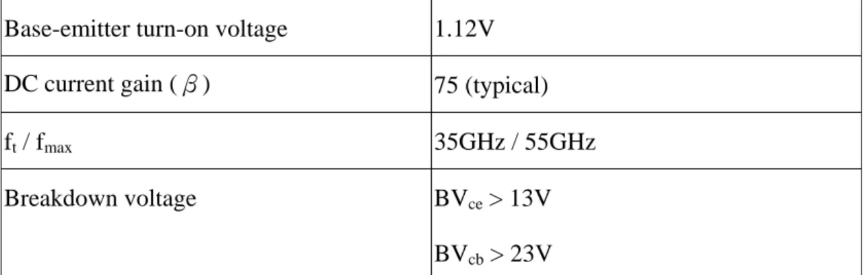
doping level to further increase the breakdown voltages, BVce and BVcb.
Base-emitter turn-on voltage 1.12V
DC current gain (β) 75 (typical)
ft / fmax 35GHz / 55GHz
Breakdown voltage BVce > 13V
BVcb > 23V
Table 2.1 Performance of GCTC HBT
2-3 Basic Darlington cell
A basic Darlington cell and the corresponding AC currents are shown as Fig.2-3.
R
biasI
iβ
acI
iβ
acI
x/(β
ac+
1)
I
x(β
ac+1)I
iI
x/(β
ac+1)
I
oQ
1Q
2Fig.2-3 Basic Darlington cell
The primary advantage of the Darlington cell is that: an appropriate choice for
resistor Rbias yields twice the cutoff frequency (ft) of a single common-emitter
The low frequency voltage gain of a simple common emitter amplifier is
proportional to the ac beta βac of the transistor. The low frequency ac beta of the
transistor can be characterized by a dominant pole approximation given by
( ) 0 1 a c s s β
β
β
ω
= + (2-2)where ωβ is the 3-dB bandwidth of the ac current gain. The cutoff frequency ωt is
related toωβ,
ω
t =β ω
0× β (2-3) From Fig.2-3, the effective ac current gain of the Darlington cell, βeff, can beapproximated as
(
1)
2
(
2)
o ac eff ac ac ac i acI
I
β
β
β
β
β
β
+
=
=
+
≈
+
(2-4)This equation occurs when the resistor Rbias is adjusted so that the ac current
through Rbias is equal to the ac current in the emitter of Q2. Under this condition, the
Darlington cell can have an effective cutoff frequency of (2β0 × ωβ), which twice
that of a single transistor. Therefore, the Darlington cell significantly improves the gain-bandwidth product of the common emitter amplifier topology.
Besides, the Darlington cell also provides larger input impedance. According to the resistance reflection rule, the input impedance looking into the base of Q1 is
R
in=
(
β
+
1)(
r
e1+
R
bias||
r
π2)
≈
(
β
+
1)(
r
e1+
R
bias)
(2-5)Output impedance is approximately (ro1 || ro2), where ro1 and ro2 are the output
resistances due to the Early effect. Therefore, both input and output impedances are relatively large compared to 50Ω. How to achieve input and output matching simultaneously will be discussed in next section.
2-4 Input and output matching
Elementary wideband amplifier topologies, such as the common-emitter, always
use two methods for input matching: put (1) a shunt input resistor as Fig.2-4 (a) or (2)
a common-base transistor at input as Fig.2-4 (b).
Zin
Ri = Rs Zin
(a) (b)
Fig.2-4 (a) A shunt input resistor for input matching (b) A common-base transistor for input matching
For Fig.2-4 (a), the input impedance looking into the base of a common-emitter
transistor is very large compared to 50Ω. It is quite straightforward to put a 50Ω
resistor across the input terminals. Unfortunately, this impedance-matching resistor
also adds as much equivalent noise as that of the source resistance and produces a
very high noise figure.
As for the configuration in Fig.2-4 (b), the resistance looking into the emitter is
approximately equal to 1/gm, where gm is the transconductance of the common-base
transistor. It follows that a proper choice of the bias current can provide the desired
input resistance. However, this bias condition is usually far from the optimum noise
In contrast with the open-loop architecture, negative feedback can break the
trade-off between source impedance match and noise performance. A useful wideband
amplifier topology is illustrated as Fig.2-5.
R
FZin
Fig.2-5 A negative feedback resistor for input matching
A resistor RF is inserted to provide shunt feedback. The input impedance is given
as:
1
F i nR
R
A
β
≈
+
(2-6) where A is the amplifier’s open-loop gain and β is the feedback factor. Hence, thefeedback resistor RF becomes the dominant noise source, as well as determines the
input impedance. Simple noise analysis shows that the equivalent noise contribution
of RF is (1+Aβ) times smaller than that of source resistance. As a result, theoretically,
if the open-looped gain A is sufficient over the operating frequency band, a broadband
amplifier with low noise figure and good impedance matching could be achieved.
A Darlington feedback amplifier combines both advantages of a Darlington cell
and negative feedback technique. It can be proved the feedback resistor is able to
2-5 Darlington feedback amplifier
Rbias Q1 Q2 RF RS=R RL=R VsFig.2-6 Darlington feedback amplifier
A Darlington feedback amplifier with an AC source and terminal impedances is illustrated in Fig.2-6. Some designers also add another resistor at the emitter terminal of Q2 to introduce negative feedback and improve high frequency response, but also
degrade insertion gain at the same time. The following analysis is based on the configuration without this resistor.
At low frequency, Q1 acts as an emitter follower forcing Q2 to dominate the
effective transconductance of the circuit. Neglect Q1, the small signal model of
Fig.2-6 can be simplified as Fig.2-7.
RS=R RL=R Ri Ro RF Vs GmVin Vin +
-Rin RoutSystem impedances (RS, RL) are set to the same value R (always 50Ω). Ri can be
obtained from equation (2-5), which is much larger than R. Ro approximates (ro1 || ro2),
which is also a large value with respect to R. Gm is the transconductance of Q2.
Assume the feedback resistor RF is comparable to R, the input and output impedances
(Rin and Rout) can be expressed as:
1
F in out mR
R
R
R
G R
+
≈
≈
+
(2-7)Setting RF equal to GmR2 will make Rin and Rout approach system impedance R. Under these matched conditions, the low-frequency voltage gain is the same as the
insertion gain S21 as:
Chap.3 Circuit designs and layouts
3-1 Type I: Basic Darlington amplifier
The design methodology is described in details as follows. We start with an
expected insertion gain of 15dB. According to Equation (2.8) in the previous chapter,
the transconductance of Q2 can be calculated as 132.47mS. Then, the corresponding
bias DC current of Q2 is about 4 ~ 5mA. Referring to the design manual provided by
GCTC, the best-performance device for this biasing condition is selected. In addition,
the feedback resistor is set to GmR2, 330Ω, and the DC bias current of Q1 is initially
set to 1mA.
The simulation result of this initial guess is shown in Fig.3-1.
m1 freq= dB(S(2,1))=14.5790.0000 Hz m3 freq= dB(S(1,1))=-30.2430.0000 Hz m2 freq= dB(S(2,2))=-30.0020.0000 Hz 2 4 6 8 10 12 14 0 16 -30 -20 -10 0 10 -40 20 freq, GHz d B (S (2 ,1 )) m1 d B (S (1 ,1 )) m3 d B (S (2 ,2 )) m2
In Fig.3-1, at DC condition, the insertion gain is very close to the expected value
15dB. The first emitter follower stage accounts for the slight difference between the
expected value (15dB) and the simulation result (14.579dB). Both input and output
return losses are about –30dB without matching circuits.
However, since the 3dB-bandwidth is expected to cover 3.1 ~ 10.6GHz (UWB),
the values of the bias resistor and the feedback resistor need to be modified. After
tuning, the optimal schematic of the circuit is shown in Fig.3-2.
Fig.3-2 Schematic of Type I configuration
In Fig.3-2, the biasing condition is also annotated. The total power consumption
is 49.25mW. The DC power supply is set to be a normal value, 5V. A 230Ω resistor,
rather than a choke inductor, is used to provide proper biasing conditions for two
Darlington connected transistors. It is because: (1) an on-chip inductor will occupy a
very large area, and (2) the 230Ω resistor, which introduces much less noise than the
The simulation result is illustrated in Fig.3-3. m3 freq= dB(S(1,1))=-9.43114.00GHz m1 freq= dB(S(2,1))=11.4621.000GHz m2 freq= dB(S(2,1))=8.61515.00GHz m3 freq= dB(S(1,1))=-9.43114.00GHz m1 freq= dB(S(2,1))=11.4621.000GHz m2 freq= dB(S(2,1))=8.61515.00GHz 2 4 6 8 10 12 14 0 16 -40 -30 -20 -10 0 10 -50 20 freq, GHz dB (S (1 ,1 )) m3 dB (S (2 ,1 )) m1 m2 dB (S (2 ,2 ))
Fig.3-3 Simulation result of Type I configuration
After setting the current through Q1 to 6.66mA, the insertion gain is much flatter
and the 3-dB bandwidth is extended to about 15GHz. The output return loss is less than –15dB, and the input return loss degrades to about –9.5dB in 10 ~ 15GHz.
The noise figure is listed in Fig.3-4.
freq 0.0000 Hz 1.000GHz 2.000GHz 3.000GHz 4.000GHz 5.000GHz 6.000GHz 7.000GHz 8.000GHz 9.000GHz 10.00GHz 11.00GHz 12.00GHz 13.00GHz 14.00GHz 15.00GHz NFmin 4.769 4.797 4.881 5.014 5.188 5.393 5.620 5.863 6.113 6.366 6.619 6.868 7.112 7.348 7.577 7.797 nf(2) 5.278 5.298 5.355 5.449 5.575 5.729 5.906 6.100 6.308 6.525 6.747 6.970 7.192 7.412 7.626 7.835
According to the simulation results, this configuration has two obvious
drawbacks: relatively large power consumption and poor noise figure. The following
two sections provide some methods for improving of these drawbacks.
3-2 Type II: Darlington amplifier with an active load
As mentioned in the previous section, the basic configuration consumes a lot of
power. In this section, a transistor where its base and collector are connected
substitutes the 200Ω resistor. The schematic circuit with corresponding biasing
condition is shown in Fig.3-5.
Fig.3-5 Schematic of Type II configuration
The simulation result and noise figure are shown in Fig.3-6 and Fig.3-7,
m4 freq= dB(S(1,1))=-14.24715.00GHz m1 freq= dB(S(2,1))=11.9603.100GHz m2 freq= dB(S(2,1))=8.95610.60GHz m3 freq= dB(S(2,1))=7.03415.00GHz m4 freq= dB(S(1,1))=-14.24715.00GHz m1 freq= dB(S(2,1))=11.9603.100GHz m2 freq= dB(S(2,1))=8.95610.60GHz m3 freq= dB(S(2,1))=7.03415.00GHz 2 4 6 8 10 12 14 0 16 -30 -20 -10 0 10 -40 20 freq, GHz d B (S(1 ,1 )) m4 d B (S(2 ,1 )) m1 m2 m3 d B (S(2 ,2 ))
Fig.3-6 Simulation result of Type II configuration
freq 0.0000 Hz 1.000GHz 2.000GHz 3.000GHz 4.000GHz 5.000GHz 6.000GHz 7.000GHz 8.000GHz 9.000GHz 10.00GHz 11.00GHz 12.00GHz 13.00GHz 14.00GHz 15.00GHz NFmin 5.147 5.173 5.249 5.366 5.514 5.681 5.859 6.042 6.223 6.402 6.577 6.747 6.912 7.072 7.229 7.382 nf(2) 6.014 6.028 6.069 6.135 6.220 6.322 6.435 6.556 6.683 6.813 6.944 7.077 7.211 7.345 7.478 7.612
Fig.3-7 Noise figure of Type II configuration
This configuration consumes 38.3mW, which saves almost 25% power compared with the basic type. Nevertheless, the flatness of insertion gain is heavily influenced, and the 3-dB bandwidth shrinks to about 10GHz. In 3.1 ~ 10.6GHz frequency band,
the average insertion gain is still about 10.5dB, and the noise figure is similarly poor.
3-3 Type III: Darlington amplifier with parallel
output stage
As mentioned in the previous sections, the biasing condition of Q2 (the output
stage) dominates the insertion gain while that of Q1 (the first stage) influences the
flatness. In this section, the DC current through Q2 is equalized to several parallel
transistors. Considering the magnitude and the flatness of insertion gain, the number
of these parallel transistors should be carefully selected. After the observation, the
number is set to be three, and the schematic circuit is shown in Fig.3-8
The simulation result and noise figure are in Fig.3-9 and Fig.3-10, respectively. m4 freq= dB(S(1,1))=-13.67014.00GHz m1 freq= dB(S(2,1))=13.8146.000GHz m2 freq= dB(S(2,1))=10.81914.00GHz m3 freq= dB(S(2,2))=-11.6981.200GHz m4 freq= dB(S(1,1))=-13.67014.00GHz m1 freq= dB(S(2,1))=13.8146.000GHz m2 freq= dB(S(2,1))=10.81914.00GHz m3 freq= dB(S(2,2))=-11.6981.200GHz 2 4 6 8 10 12 14 0 16 -20 -10 0 10 -30 20 freq, GHz d B (S (1 ,1 )) m4 d B (S (2 ,1 )) m1 m2 d B (S (2 ,2 )) m3
Fig.3-9 Simulation result of Type III configuration
freq 0.0000 Hz 1.000GHz 2.000GHz 3.000GHz 4.000GHz 5.000GHz 6.000GHz 7.000GHz 8.000GHz 9.000GHz 10.00GHz 11.00GHz 12.00GHz 13.00GHz 14.00GHz 15.00GHz NFmin 4.198 4.215 4.266 4.348 4.459 4.592 4.745 4.914 5.093 5.281 5.474 5.670 5.867 6.064 6.260 6.453 nf(2) 4.441 4.454 4.494 4.559 4.649 4.759 4.889 5.035 5.195 5.366 5.546 5.731 5.921 6.113 6.305 6.498
Fig.3-10 Noise figure of Type III configuration
both input and output return loss maintain below –10dB.
The noise figure of Darlington feedback structure is relatively high (reported
5-6dB at 10GHz in [1]), because that feedback resistor unavoidably introduces the
input noise to the output. Besides, noises coming from devices also should be
considered. In Type III configuration, paralleling these transistors is equivalent to
paralleling these corresponding noise sources, leading to a smaller noise source and
indirectly improving the noise figure. Compare Fig.3-10 with Fig.3-4, paralleling
three transistors at the output stage improves the noise figure of about 1dB.
3-4 Type IV: Cascade Darlington amplifier
This configuration simply cascades two Darlington amplifiers. Since both input
and output are well matched to 50Ω, two Darlington feedback amplifiers are
connected directly. The schematic is shown in Fig.3-11.
The simulation result and the noise figure are in Fig.3-12 and Fig.3-13, respectively. m1 freq= dB(S(2,1))=18.6396.400GHz m2 freq= dB(S(2,1))=15.70415.00GHz m3 freq= dB(S(1,1))=-10.16614.00GHz m1 freq= dB(S(2,1))=18.6396.400GHz m2 freq= dB(S(2,1))=15.70415.00GHz m3 freq= dB(S(1,1))=-10.16614.00GHz 2 4 6 8 10 12 14 0 16 -10 0 10 -20 20 freq, GHz d B (S (2 ,1 )) m1 m2 d B (S (1 ,1 )) m3 d B (S (2 ,2 ))
Fig.3-12 Simulation result of Type IV configuration
freq 0.0000 Hz 1.000GHz 2.000GHz 3.000GHz 4.000GHz 5.000GHz 6.000GHz 7.000GHz 8.000GHz 9.000GHz 10.00GHz 11.00GHz 12.00GHz 13.00GHz 14.00GHz 15.00GHz NFmin 5.975 5.999 6.069 6.182 6.331 6.509 6.710 6.926 7.153 7.386 7.623 7.861 8.098 8.334 8.568 8.800 nf(2) 6.355 6.374 6.430 6.522 6.644 6.793 6.963 7.151 7.351 7.560 7.775 7.994 8.215 8.437 8.660 8.883
Fig.3-13 Noise figure of Type IV configuration
These two feedback resistors are set to be 250Ω as considering of the flatness of
figure degrades about 1dB than that of a single-stage one. Power consumption is
almost twice while insertion gain boosts up of about 5dB.
3-5 Layouts
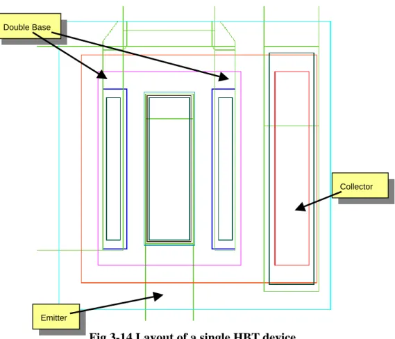
The layout of a HBT device is shown in Fig.3-14.
Fig.3-14 Layout of a single HBT device
Metal 1 is used to interconnect the primary circuit elements. A length of metal
could be considered as a microstrip line with substrate thickness of 100µm and dielectric constant of 12.9 (εr = 12.9 for GaAs). The width of a 50Ω microstrip line
is about 73 µm. Since the width of base (about 20μm) is much smaller than 73 µm, a “stepwise” layout, as shown in Fig.3-15 on next page, is used to feed the RF signals.
Double Base
Emitter
Fig.3-15 Layout of an AC feeding structure
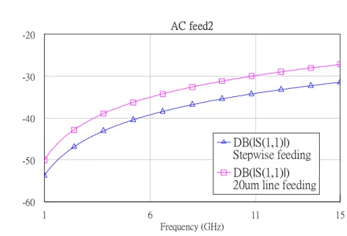
Fig.3-16 and Fig.3-17 show the comparisons of insertion loss and return loss
between a stepwise structure and a feeding line of 20μm in width.
1 6 11 15 Frequency (GHz) AC feed1 -0.025 -0.02 -0.015 -0.01 -0.005 DB(|S(2,1)|) Stepwise feeding DB(|S(2,1)|) 20um line feeding
1 6 11 15 Frequency (GHz) AC feed2 -60 -50 -40 -30 -20 DB(|S(1,1)|) Stepwise feeding DB(|S(1,1)|) 20um line feeding
Fig.3-17 Comparison of return loss
It is obvious that a stepwise structure (“△” dots) provides lower insertion loss
and better return loss.
There is another important issue: current density. It governs the sizes of
interconnecting metals and thin film resistors. The table below lists some relative
design rules.
Metal 1 Metal 2 Thin film resistor
Min. width 2μm 2μm 1.4μm
Min. spacing 2μm 2μm 2μm
Max. current density 3mA/μm of width 5mA/μm of width 1mA/μm of width
Sheet resistance 50Ω/square
According to Table 3-1 and DC currents annotated in the schematics of four
configurations, the sizes of resistors and interconnecting metal can be decided. The
layout of Type I configuration is shown in Fig.3-18.
Fig.3-18 Layout of Type I configuration
Fig. 3-19 shows the enlarged view of central part of Fig. 3-18.
Fig.3-19 Central part of Type I configuration
230 ohm W = 15 um 200 ohm W = 10 um 300 ohm W = 2 um Spacing = 10 um Backside Via
In Fig.3-18, the backside via provides electrical contact between metals and the
ground plane. The distance between the central part and the backside pad is 20μm,
which is a little longer than the minimum space, 15μm. The spacing between two
HBT devices is kept to be 10μm. The widths (in μm) of thin film resistors are
chosen to handle 1.5 times (in mA) of the corresponding DC currents.
The overall layout of Type II configuration is shown in Fig.3-20 and the central
part is zoomed in Fig.3-21.
Fig.3-20 Layout of Type II configuration
Fig.3-21 Central part of Type II configuration
300 ohm
W = 2 um
300 ohm
The overall layout of Type III structure is shown in Fig.3-22 and the central part
is zoomed in Fig.3-23.
Fig.3-22 Layout of Type III configuration
Fig.3-23 Central part of Type III configuration
The bases and emitters of three transistors are connected together through silicon
nitride vias between metal 1 and metal 2. A more detailed view is shown in Fig.3-24
on next page. 250 ohm W =2 um 240 ohm W =10 um 220 ohm W =20 um
Fig.3-24 Metal 1 and Metal 2
The sizes of vias are set to minimum (1.6μm × 1.6μm). The widths of two
parallel metal 2 are both 3μm, and the spacing is 10μm. The relatively large spacing
(compared with line width) can avoid unwanted coupling and feedback effects.
The Type I, II, III configurations occupies no more than 550 μm × 350 μm
of chip area.
The overall layout of Type IV structure is shown in Fig.3-25 and the central part
is zoomed in Fig.3-26.
Fig.3-25 Layout of Type IV configuration
Spacing = 10 um
Fig.3-26 Central part of Type IV configuration
3-6 Modified simulation results
The arrangement of layouts will significantly influence measurement results,
especially the emitter-to-ground metals. These connecting metals can be
approximately equivalent to inductors. It is known that ground inductors definitely
have great effects on the stability and high frequency performance. As a result, these
metals must be taken into account.
An EM simulator (Sonnet9.52) is utilized to simulate ground metals and then
export to a “.sp file”. These files are used to modify ordinary simulation results. For
example, reconsider Type I configuration. After the layout is fixed, the ground metal 250 ohm W =2 um 200 ohm W =10 um 272 ohm W =15 um 235 ohm W =15 um
is drawn (by Sonnet9.52) as Fig.3-27.
Fig.3-27 Ground metal drawn by Sonnet9.52
The practical ground metal is shown in Fig.3-28.
Fig.3-28 Practical ground metal
transistor. Port 2 corresponds the ground pad, and Port 3 de-embeds to the joint of the
biasing resistor. Since the thickness of metal 1 is much greater than the upper
dielectric layer (silicon nitride), the “Thick Metal” model provided by Sonnet9.52 is
utilized for a more precise simulation results.
After including the ground metal effect (as in Fig.3-29), the modified simulation
result of Type I configuration is shown in Fig.3-30.
Fig.3-29 Schematic with ground metal model
m3 freq= dB(S(1,1))=-9.06313.50GHz m2 freq= dB(S(2,1))=7.93315.00GHz m3 freq= dB(S(1,1))=-9.06313.50GHz m1 freq= dB(S(2,1))=11.3221.000GHz m2 freq= dB(S(2,1))=7.93315.00GHz 2 4 6 8 10 12 14 0 16 -40 -20 0 -60 20 freq, GHz dB (S (1 ,1 )) m3 dB (S (2 ,1 )) m1 m2 dB (S (2 ,2 )) m1 freq= dB(S(2,1))=11.3221.000GHz
Fig.3-30 Modified simulation result of Type I configuration
Compare Fig.3-30 with Fig.3-3, it is almost the same at low frequency while
insertion gain reduces about 0.6dB at high frequency, leading to the shrinkage of 3dB
Similarly, Fig.3-31, Fig.3-32, and Fig.3-33 show the modified simulation results
of Type II, Type III, and Type IV configurations.
m4 freq= dB(S(1,1))=-13.95015.00GHz m1 freq= dB(S(2,1))=11.8063.100GHz m2 freq= dB(S(2,1))=8.77510.60GHz m3 freq= dB(S(2,1))=6.86915.00GHz m4 freq= dB(S(1,1))=-13.95015.00GHz m1 freq= dB(S(2,1))=11.8063.100GHz m2 freq= dB(S(2,1))=8.77510.60GHz m3 freq= dB(S(2,1))=6.86915.00GHz 2 4 6 8 10 12 14 0 16 -30 -20 -10 0 10 -40 20 freq, GHz d B (S (1 ,1 )) m4 d B (S (2 ,1 )) m1 m2 m3 d B (S (2 ,2 ))
Fig.3-31 Modified simulation result of Type II configuration
m4 freq= dB(S(1,1))=-11.99514.00GHz m1 freq= dB(S(2,1))=13.0956.000GHz m2 freq= dB(S(2,1))=9.58514.00GHz m3 freq= dB(S(2,2))=-12.2251.200GHz m4 freq= dB(S(1,1))=-11.99514.00GHz m1 freq= dB(S(2,1))=13.0956.000GHz m2 freq= dB(S(2,1))=9.58514.00GHz m3 freq= dB(S(2,2))=-12.2251.200GHz 2 4 6 8 10 12 14 0 16 -20 -10 0 10 -30 20 freq, GHz d B (S (1 ,1 )) m4 d B (S (2 ,1 )) m1 m2 d B (S (2 ,2 )) m3
m1 freq= dB(S(2,1))=18.2066.000GHz m2 freq= dB(S(2,1))=14.64015.00GHz m3 freq= dB(S(1,1))=-10.25914.00GHz m1 freq= dB(S(2,1))=18.2066.000GHz m2 freq= dB(S(2,1))=14.64015.00GHz m3 freq= dB(S(1,1))=-10.25914.00GHz 2 4 6 8 10 12 14 0 16 -10 0 10 -20 20 freq, GHz d B (S (2 ,1 )) m1 m2 d B (S (1 ,1 )) m3 d B (S (2 ,2 ))
Chap.4 Measurement results and conclusions
A photograph of a circuit is shown in Fig.4-1.
Fig.4-1 Photograph of the circuit
Two 100pF capacitors are added at the input and output feeding lines.
The S-parameters and noise figures of these four configurations are presented in
Fig.4-2, Fig.4-3, Fig.4-4 and Fig.4-5, Fig.4-6, respectively.
1 6 11 15 Frequency (GHz) Darlington_basic1 -40 -30 -20 -10 0 10 20 4.33 GHz -13.71 dB 10.6 GHz -10.36 dB 10.6 GHz 9.536 dB 3.1 GHz 12.23 dB DB(|S(1,1)|) Darlington_basic1 DB(|S(2,1)|) Darlington_basic1 DB(|S(2,2)|) Darlington_basic1 DB(|S(1,2)|) Darlington_basic1 DB(|S(2,1)|) Simulation S21
Fig.4-2 S-parameter of Type I configuration
1 6 11 15 Frequency (GHz) Darlington_active2 -60 -40 -20 0 20 10.6 GHz -15.57 dB 6.03 GHz -13.86 dB 10.6 GHz 7.786 dB 3.101 GHz 12.47 dB DB(|S(1,1)|) Simulation S21 DB(|S(2,1)|) Darlington_active2 DB(|S(2,2)|) Darlington_active2 DB(|S(1,2)|) Darlington_active2 DB(|S(2,1)|) Dar_active
Fig.4-3 S-parameter of Type II configuration
1 6 11 15 Frequency (GHz) Darlington_par2 -40 -30 -20 -10 0 10 20 10.6 GHz 8.947 dB 3.1 GHz 13.16 dB 4.4 GHz -9.961 dB 6 GHz -13.84 dB DB(|S(1,1)|) Darlington_par2 DB(|S(2,1)|) Darlington_par2 DB(|S(2,2)|) Darlington_par2 DB(|S(1,2)|) Darlington_par2 DB(|S(2,1)|) Simulation S21
1 6 11 15 Frequency (GHz) Darlington_cas2 -60 -30 0 30 7.13 GHz -5.608 dB 5.73 GHz -3.389 dB 10.6 GHz 18.7 dB 3.1 GHz 25.08 dB DB(|S(1,1)|) Simulation S21 DB(|S(2,1)|) Darlington_cas2 DB(|S(2,2)|) Darlington_cas2 DB(|S(1,2)|) Darlington_cas2 DB(|S(2,1)|) Dar_cas
Fig.4-5 S-parameter of Type IV configuration
Noise Figure 0 2 4 6 8 10 0 5 10 15 20 Frequency (GHz) dB Parallel Basic Active Cascade
Fig.4-6 Noise figures of four configurations
Generally, except for Type IV configuration, the insertion gains at low frequency are close to simulation results. Type I configuration has a smooth insertion gain. Type
II configuration consumes less power but has a poor noise figure. Type III
configuration has larger insertion gain and better noise performance.
Amazingly, the insertion gain and noise figure of Type IV configuration is
superior to simulation results, while return loss degrades to about –3.4~-5dB. I think it
Reference
[1] K. Kobayashi, R. Esfandiari, A. Oki, D. Umemoto, J. Camou, M. Kim
“GaAs heterojunction bipolar transistor MMIC DC to 10 GHz direct-coupled feedback amplifier”
Gallium Arsenide Integrated Circuit (GaAs IC) Symposium, 1989. Technical Digest 1989. 11th Annual 22-25 Oct. 1989 Page(s):87 – 90.
[2] K. Kobayashi, D. Umemoto, R. Esfandiari, A. Oki, L. Pawlowicz, M. Hafizi, L. Tran, J. Camou, K. Stolt, D. Streit, M. Kim
“GaAs HBT MMIC broadband amplifiers from DC to 20 GHz”
Microwave and Millimeter-Wave Monolithic Circuits Symposium, 1990. Digest of Papers, IEEE 1990 7-8 May 1990 Page(s):19 – 22.
[3] K. Kobayashi, A. Oki
“A low-noise baseband 5-GHz direct-coupled HBT amplifier with common-base
active input match”
Microwave and Guided Wave Letters, IEEE [see also IEEE Microwave and Wireless Components Letters] Volume 4, Issue 11, Nov. 1994 Page(s):373 – 375
[4] K. Kobayashi, R. Esfandiari, M. Hafizi, D. Streit, A. Oki, L. Tran, D. Umemoto, M. Kim
“GaAs HBT wideband matrix distributed and Darlington feedback amplifiers to 24 GHz”
Microwave Theory and Techniques, IEEE Transactions on Volume 39, Issue 12, Dec 1991 Page(s):2001 – 2009
[5] C. Armijo, R. Meyer
“A new wide-band Darlington amplifier”
Solid-State Circuits, IEEE Journal of Volume 24, Issue 4, Aug. 1989 Page(s):1105 - 1109
[6] D. Cui, D. Sawdai, S. Hsu, D. Pavlidis
“Low DC power, high gain-bandwidth product, coplanar Darlington feedback
amplifiers using InAlAs/InGaAs heterojunction bipolar transistors”
Annual5-8 Nov 2000 Page(s):259 - 262
[7] N. Sheng, W. Ho, N. Wang, R. Pierson, P. Asbeck, W. Edwards
“A 30 GHz bandwidth AlGaAs-GaAs HBT direct-coupled feedback amplifier” Microwave and Guided Wave Letters, IEEE [see also IEEE Microwave and
Wireless Components Letters] Volume 1, Issue 8, Aug. 1991 Page(s):208 – 210
[8] Y. Kuriyama, J. Akagi, T. Sugiyama, S. Hongo, K. Tsuda, N. Iizuka, M. Obara “DC to 40-GHz broad-band amplifiers using AlGaAs/GaAs HBT's”
Solid-State Circuits, IEEE Journal of Volume 30, Issue 10, Oct. 1995 Page(s):1051 - 1054
[9] Bo Shi, Yan Wah Chia
“Design of a SiGe low-noise amplifier for 3.1-10.6 GHz ultra-wideband radio” Circuits and Systems, 2004. ISCAS '04. Proceedings of the 2004 International
Symposium on Volume 1, 23-26 May 2004 Page(s):I-101 - I-104 Vol.1
[10] Power HBT Design Manual of GCTC
[11] M.F. Chang
“Current trends in heterojunction bipolar transistors”, World Scientific Publishing Co.
[12] D. Pozar