國立交通大學
機械工程學系
博士論文
抓爬式靜電微致動器之模擬及
低電壓區輸出特性的改善
Modeling of Scratch Drive Actuator and
Performance Enhancement
in Low-Voltage Region
研 究 生:
陳 雄 章
指導教授:
徐 文 祥 博士
抓爬式靜電微致動器之模擬及
低電壓區輸出特性的改善
Modeling of Scratch Drive Actuator and
Performance Enhancement
in Low-Voltage Region
研 究 生:陳雄章
Student: Shawn Chen
指導教授:徐文祥
Advisor: Wensyang Hsu
國 立 交 通 大 學
機 械 工 程 學 系
博 士 論 文
ADissertationSubmitted to Department of Mechanical Engineering College of Engineering
National Chiao Tung University in partial Fulfillment of the Requirements
for the Degree of PhD in
Mechanical Engineering
Modeling of Scratch Drive Actuator and Performance
Enhancement in Low-Voltage Region
Student:Shawn Chen Advisor:Wensyang Hsu
Department of Mechanical Engineering
National Chiao Tung University
Abstract
An improved model is proposed to reduce the cost due to trial and error in selection of Scratch Drive Actuator (SDA) geometry, driving voltage and output force level. Besides, a novel SDA design to reduce driving voltage from at least 80 volts to 40 volts to get better reliability with comparable output is also proposed. It is assumed that the deformation and property of SDA is same along the width direction, as the main plate may be treated by a beam model. Governing equation based on Euler-Bernoulli beam is first constructed. Solving this equation with proper boundary conditions, key SDA characteristics can be determined analytically, such as non-contact length, priming voltage, deflection curve, output force, bending moment and stress. The output force just stated is the input of SDA dynamic model of single degree-of-freedom including friction. To verify proposed model, electroplated nickel SDA arrays of 80 µm in length and 65 µm in width with suspended spring are fabricated and tested. The average travel distance after 1500 input pulses from 80 to 120 volts are measured to be from 5.9 to 13.9 µm, while average measured output forces are from 12.4 to 30.2 µN per SDA. Deviations between simulated and measured results are less than 10%, showing the superior ability of the proposed integrated SDA model for better performance prediction.
A low-voltage scratch drive actuator (LVSDA) is also proposed here by incorporating flexible joint into the conventional rectangular SDA to improve performance in low-voltage region. Experimental results show that, at the same total plate length of 80 µm and width of 65 µm, the proposed LVSDA can be actuated as low as 40 volts, much lower than 80 volts, the minimum required input voltage of conventional SDA. From nonlinear finite element analysis conducted by CosmosWorks, yielding effect is found to be a critical factor. Before yielding, LVSDA can provide better performance than SDA at the same input voltage. However, the yielding stress in flexible joint would limit the achievable maximum output force in high-voltage region. By varying joint length, width, or location, LVSDA has been operated in low-voltage region where the conventional SDA can not be operated, and can still provide comparable performance as SDA in high-voltage region. The proposed LVSDA design can provide more flexibility in design selection to meet different performance requirements.
抓爬式靜電微致動器之模擬及低電壓區輸出特性的改善
學生:陳雄章 指導教授:徐文祥
國立交通大學機械工程學系
摘 要
抓爬式靜電微致動器(SDA)有微牛頓等級輸出力、在數十奈米等級步進尺寸下可行 進達數毫米。 迄今,此類致動器的幾何尺寸選擇主要依賴經驗,驅動電壓及輸出力亦需 經由實驗測試後方有依據。為減少試誤法造成成本負擔,發展系統化的解析模型有其必 要性。此外傳統矩形抓爬式微致動器的啟動電壓常超過 80 伏特,容易造成介電層崩潰 之可靠度問題。因此開發新設計以降低操作電壓、能源消耗、並維持足夠輸出力及可靠 度是另一研究重點。 本研究第一部份旨在建立抓爬式微致動器的較符合現實情況之解析模型,並以面型 鎳基微加工技術製作。由於抓爬式微致動器的運動以單一方向為主,假設其沿寬度方向 的變形及應力分佈一致;因此可依據 Euler-Bernoulli 樑的模型,配合適當的邊界條件以 解出相關的積分常數,再依序推導如未接觸長度、貼底(priming)電壓、變形曲線、輸出 力、彎矩及最大正向應力等特徵。上述輸出力可設為單自由度運動方程式的輸入。在長 80 微米、寬 65 微米的尺寸下,以 80 到 120 伏特為輸入範圍,其步進尺寸預測值在 22 到 41 奈米之間。以 500Hz 電壓測試結果發現,1500 次輸入脈波所得總行程位移介於 5.9 到 13.9 微米;每個抓爬式微致動器輸出力介於 12.4 到 30.2 微牛頓,其測試結果與預測 值誤差小於 10%,顯示本文提出之解析模型具有可預測輸出力的較佳實用性。 本研究第二部份提出一種新式可在較低電壓驅動的抓爬式微致動器設計,主要是將 撓性接頭加入傳統矩形板的中間適當處。在同樣總長 80 微米和寬 65 微米的尺寸下,製 作並測試具有不同撓性接頭尺寸及位置的設計,其結果發現啟動電壓最小可降低到約 40 伏,遠低於傳統同尺寸抓爬式微致動器所需要的 80 伏特。當輸入電壓在 40 到 120 伏之 間時,其步進尺寸預測值在 9 到 67 奈米之間,而實測輸出力在 4.9 到 19.6 微牛頓之間。 證實所提出的新設計可在傳統抓爬式微致動器無法操作的低電壓區有效操作。但有限元 素法分析結果亦顯示,在高電壓區的最大輸出力,會受到撓性接頭最大應力達到降伏應 力的限制。在此提出的融合撓性接頭的設計,將可提供抓爬式微致動器更大的設計空誌 謝
謝天謝地謝謝你, 感謝關心與督促。 特別感謝指導教授徐文祥博士。 他的美式風格如當頭棒喝讓我頓悟覺醒,終能修成 正果,體會作研究的精義、寫論文的方法及待人處世之道。佩服、值得。 感謝交大老師們的無私教誨及傾囊相授,讓我見識理解到教學和研究的典範。 感謝中央大學王國雄教授。在我就讀中大碩士班的指導與提攜,讓我了解學術殿堂 的訣竅與奧妙。在交大博士班修業期間,也常鼓勵並提醒相關研究的重點;使我能 在關鍵時刻做出恰當的判斷。 感謝各位口試委員教授們的肯定及愷切指導;讓我能將論文修正到更為嚴謹週延。 且在研究的未來方向確認出較佳的切入點。 謝謝同門師兄弟的切磋及協助,終於完成博士班的研究訓練。 最要感謝家維學弟在製程及測試的努力與投入,這是我們共同分享的榮耀,Hokila! 感謝內人妙芳的愛與全力支持、父母的養育教導,家人的體貼包容讓我安心完成學 業。我愛你們。 終於、 我畢業了。山又是山、水又是水;肩頭上多的是 責任,心裡多的是 理想。 如何在各項拘束之間取得平衡,這是一個 重要的課題! 風城的各位,有空到文化城台中說新敘舊、煮酒泡茶、點子就誕生了。再會。 雄章 于 新竹交通大學 2010.07.13CONTENTS
Abstract I Chinese Abstract II Acknowledgements III Figure List VI Table List VIII Notation IX
Chapter 1 Introduction 1
1.1 Motivation 1
1.2 Literature review 1
1.3 Goals 4
1.4 Approach in this study 5
Chapter 2 Modeling of Scratch Drive Actuator 11
2.1 Operation principle of SDA 11
2.2 Static analysis of SDA 11
2.3 Dynamic analysis of SDA 18
Chapter 3 Performance Enhancement of Scratch Drive Actuator with Modified Flexible Joint 24
3.1 Concept design of low volatge Scratch Drive Actuator (LVSDA) 24
3.2 Qualitative analysis 25
3.3 Finite element analysis 26
Chapter 4 Fabrications and Results 34
4.2 Analytical and testing results of SDA 39
4.3 FEA and testing results of LVSDA 55
Chapter 5 Conclusions 63 5.1 Summary 63 5.2 Future work 64 References 69 Publication List 74 Chinese Vita 75
Figure List
Figure 1-1 Operation principles of SDA 7
Figure 1-2 Typical applications of SDA in microelectromechanical system 8
Figure 1-3 Step size estimated from experimental results in Akiyama’s work 9
Figure 1-4 Step size estimated from experimental results in Langlet’s work 9
Figure 1-5 Step size predicted from analytical model in Kazuaki’s work 9
Figure 1-6 Snap through and priming voltages predicted from analytical model in Linderman’s work 9
Figure 1-7 Output force estimation methods 10
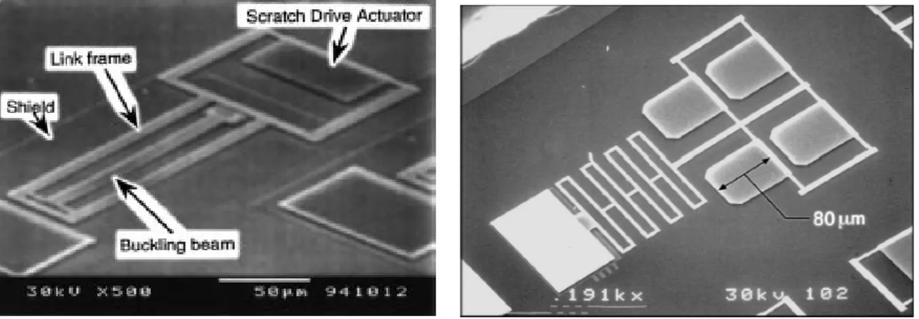
Figure 2-1 Structures and elements of SDA 20
Figure 2-2 Five states in SDA operation at different input voltages 21
Figure 2-3 Coordinate system and electrostatic force in post-priming configuration 22
Figure 2-4 Step size of SDA operated in fully-discharge mode 22
Figure 2-5 Step size of SDA operated in constantly-contact mode 23
Figure 3-1 Concept design of low-voltage Scratch Drive Actuator with flexible joint 28
Figure 3-2 Operation procedures of conventional SDA and LVSDA 28
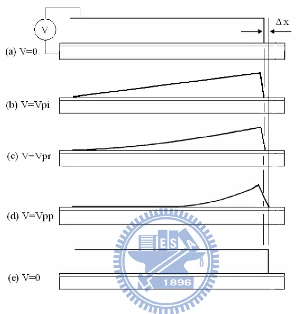
Figure 3-3 Design layout of micro-electroplated nickel SDA 29
Figure 3-4 Qualitative analysis on flexible joint effect 30
Figure 3-5 Finite Element Analysis (FEA) results of LVSDA 31
Figure 4-1 Fabrication process of micro-electroplated nickel SDA 36
Figure 4-2 SEM pictures of fabricated results 38
Figure 4-3 Driving test of released devices 38
Figure 4-4 Non-contact length of SDA vs. input voltage 45
Figure 4-5 Simulated results on priming voltage 45
Figure 4-6 Simulated results on step size 46
Figure 4-7 Simulated results on maximum bending moment and stress 47
Figure 4-9 SDOF and Simulink models of SDA 49
Figure 4-10 Effects of viscous damping on displacement response 50
Figure 4-11 Effects of Coulomb offset on displacement response 51
Figure 4-12 Matching the dynamical parameters by Simulink model 52
Figure 4-13 Measured and simulated total travel distances 53
Figure 4-14 Output force plot of experimental and simulated results 54
Figure 4-15 Driving test and measurement of device LV-10-20-50-6 59
Figure 4-16 Effects of scratch plate length 60
Figure 4-17 Effects of flexible joint width and length 61
Figure 4-18 Simulated maximum stresses of device series LV-15-15-50-Wj 62
Figure 5-1 Contact and Non-contact length for different plate length 68
Table List
Table 1-1 Summary of previous researches on SDA modeling 10
Table 3-1 Notation of LVSDA testing types 32
Table 3-2 Simulation parameters for FEA 33
Table 4-1 Lithography parameters 37
Notation
Vpi Pull-in voltage
Vpr Priming voltage
Vpp Post-priming voltage
Zb, Zn Bushing height and thickness of dielectric layer, respectively
Zm Constant equal to Zb+ Zn
q Distributed load
ε0 Permittivity of air;
κ, κ1 Relative dielectric constant
V Input voltage
W Plate width
d Gap distance between two plates
y Main beam deflection
∆x Step size
l SDA plate length
h Bushing height
Ud Elastic energy of bending
Us Electrostatic energy of capacitor
UT Total energy
l' Contact length of plate with dielectrics
L’’ Plate length
L’ Measured contact length of plate
xb(L’) Bushing position at L’
a Thickness t of the dielectric layer divided by the relative permittivity κ
b Equal to h / ln2
ln Non-contact length of main beam at the given input voltage
E Young’s modulus of SDA material
I Second area moment of main beam
x Horizontal coordinate of the element in consideration
c1, c2, c3, c4 Integration constants
kt Torsional spring constant of support beam
β Aspect ratio constant based on ratio of width to thickness of support beam
Wp Width of support beam
Lp Length of support beam
G Shear modulus of SDA material
M Bending moment at position x in non-contact part of main beam
Mmax Maximum moment
xmax Position the maximum moment Mmax happens along main beam for an input
σmax Maximum bending stress along main beam for an input
Fo Horizontal output force of charged SDA array
N SDA number in the SDA array
θ Angle between the horizontal and the tangent line along main beam
∆x1, ∆x2 Backward displacement of bushing top at pull-in and (post) priming respectively
∆xpr, ∆xpp Step size at priming voltage and post priming voltage, respectively
m Lump-mass of SDA or LVSDA array including the ring
k Spring constant of suspended tether spring
µ Coulomb friction coefficient between contact surfaces
FN Normal force between contact surfaces
ω Αngular velocity of sinusoidal driving voltage
σe, σy, σult Endurance limit, yielding stress, and ultimate stress, respectively
σmax, σmin Maximum and minimum bending stress, respectively
σav, σr Average and range of bending stress, respectively
σR Equivalent fully-reverse stress amplitude of same fatigue life
Lm, Ls Main plate length and scratch plate length in LVSDA, respectively
Lj, Wj Length and width of flexible joint in LVSDA, respectively
k1 Spring constant of one box spring
Lr, Wr Half length and width of box spring, respectively
FE Equivalent electrostatic force
A, B Characteristic coefficients in Basquin’s equation
∆x0 Step size with zero spring load
∆x(n) Step size at nth input pulse
Chapter 1 Introduction
Regular micro actuators can perform nano/micro-meter scale resolution displacement and
micro-Newton scale output force. Electrostatic microactuators produce relative high output
force per unit input voltage due to their surface-force nature.
1.1 Motivation
Among them, the scratch drive actuator (SDA) is operated mainly in nonlinear manner and
in post-priming region. As shown in Figure 1-1 [1], SDA can step forward with 10~100 nm
resolution, 1 mm long travel distance and 63 µN output force per SDA at 200V. These good characteristics make the SDA competitive in the field of microactuators. In general, present
models of SDA are basically restricted in static region because the complexity from the
nonlinear coupling between the electrostatic, mechanical and friction forces. Yet, it is less
understood in the MEMS field in spite of its importance. Besides, conventional rectangular
SDA is often driven by voltage over 80 volts which is somewhat too high in electronic system.
1.2 Literature review
The scratch drive actuator (SDA) was first proposed by Akiyama and Shono to show the
controllable step-wise motion of nano-meter resolution [2, 3]. By transforming the electrostatic
energy into mechanical displacement elegantly with friction, SDA is attractive in micro or even
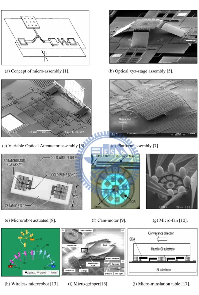
nano manipulation. Applications of SDA have been reported in many microelectromechanical
systems (MEMS), such as design of platform self-assembly [1,4], optical xyz-stage assembly
[5], variable optical attenuator (VOA) assembly by triangular SDA array [6], platform
self-assembly by buckled beam [7], microrobot actuation by large SDA array [8], operation of
micro-gripper [16], microtranslation table [17], and inverted SDA array for large area
actuation[18]. Some typical devices in these literatures are shown in Figure 1-2. Generally, the
required driving voltages in the literatures on are still very high, usually above 80 volts.
In geometrical design of SDA, different shapes on SDA main plate have been reported,
and the most common one is the rectangular shape. It was found that the output force was
proportional to the width of main plate and square of input voltage [1]. Also, a longer main
plate could reduce the minimum required driving voltage, so-called threshold voltage, to
activate the SDA [1, 8]. However, the output force of a longer SDA would be smaller than that
of a shorter SDA at the same driving voltage in general [1, 8]. Besides the rectangular shape,
triangular and trapezoidal shapes [19] also have been reported. In triangular design, the apex is
placed at the free edge of main plate. While in trapezoidal design, the wider side is placed at
free edge. The yield rates at different dimension-ratio designs were investigated, but output
forces at different designs were not mentioned [19]. For the effect on bushing height, it was
reported that a bigger step size could be achieved for a larger bushing height with the price of
higher input voltage.
Some researches attempted to explore the relation between step size and input voltage of
SDA. The step size under constant load is the most fundamental case and has been studied by
various methods. One approach was to measure the contact length of charged SDA with
insulated layer using interference image, and then calculated the step size from geometry of
selected images as in Figure 1-3 [2]. The step size may be calculated from the equation (1-1)
Step size ∆x = h2 / 2(l-l’) (1-1) where l is the SDA plate length, h is bushing height and l' is the contact length of plate by
measuring interference image. In [19], an empirical equation (1-2) is used to calculate the step
Step size ∆x = xb(L’)-xb(L’(0)) (1-2)
where L’(0) and L’ are the measured contact length at beginning xb(L’(0) and xb(L’), the latter is
the bushing position when L’. These two approaches did not relate the step size with input
voltage analytically. In [20], the energy method is used to derive and predict the step size and
non-contact length of SDA for given input by treating the reaction force at bushing as
concentrated load as shown in Figure 1-5. Since electrostatic force did exist along the main
beam in SDA operation, the predicted step size was overestimated comparing to measured
results. The results in [20] is summarized as following
Another approach used a second-order differential equation [8] to predict the snap through and
priming voltages by using square load model in Figure 1-6. The results are as following
11) -(1 )] ln 2 ) ln( ) ( tan 3 ( 24 [ voltage Priming 10) -(1 ln ) 2 / 1 ( tanh ) 2 / 3 ( 1 3 1 ln tanh 3 3 2 6 voltage in) -(pull through Snap 2 1 1 4 2 2 2 1 2 1 1 1 2 1 n n b b n b n b b n pr m m m m m m m m m m m m m pi Z Z Z Z Z Z Z Z Z Z W L EI Z V ) d/Z (Z d Z d d Z d d) /Z L))( K/Z ( /d) (( )]} d/Z (Z Z d ) Z d ( d)) (Z (Kd/L)/Z d(Z )[ dEI We {( L W EI V b − + − + = − − − − + − − − − + = − − − εκ κ εκ 9) -(1 ) 4 27 ( : size Step then ), 0 (at and 8) -(1 , ) 4 3 ( : length contact -Non 0, when and , : energy Total 7) -(1 , 2 : energy tic Electrosta 6) -(1 , ) ( : e Capacitanc ) 5 1 ( ] [ 2 : energy Elastic 4) -(1 ), 2 3 ( 2 : curve Deflection then conditins, boundary with twice g integratin 3) -(1 , : equation Governing The 4 1 3 6 4 1 2 2 3 2 0 2 2 2 3 2 3 3 2 2 V Edt h h x x dx dy V h Edt l dl dU U U U CV U d l L W C dx dx y d EI U l x l x l h y EI M dx y d T s d T s l d ε θ θ ε ε = ≅ ∆ = ≅ = = + = − = − = − = + − = − =
∫
Other works on the determination of deflection and step size [21, 22] followed basically the
piecewise combination of previous methods [2, 8, and 19] with minor modifications and the
results were like that of previous literatures. For the step size with variable load, such as SDA
connected to a suspended spring under continuous loading/unloading process, was not reported
yet. The increasing spring force will decrease the step size dynamically. As the driving voltage
continuously input, the total travel distance is accumulated also and represented the positioning
ability of SDA device.
For the determination of SDA output force, experimental approaches have been reported
mainly. These methods include buckling-load method [1] and spring-deflection method [8, 23]
as shown in Figure 1-7. The output force of SDA array in Figure 1-7(a) is expressed as the
buckling load of the slender buckle beam, which is related to the geometry, material and
constraint type of the beam. The test results [1] showed that the buckle beam sometimes
bifurcated into two different mode shapes; as a result, the output force was not easily
determined as one unique value. In Figure 1-7(b), the SDA output force is determined as the
multiplication of the spring constant and its total deflection. Arranging and classifying results
in previous literatures, some key characteristics and performances are listed in Table 1. It is
clear that till now, no analytical formulations are reported to be able to model completely both
the static and the dynamic behavior of SDA including friction effect.
1.3 Goals
From the discussion above, the goals of this work may be ascribed into two major topics.
The first one is to propose a better analytical model on SDA to improve the prediction
capability such as priming voltage, step size, total travel distance, output force and dynamic
response simulation. The second one is to propose a novel lower voltage SDA (LVSDA) design
compatibility of SDA with integrated circuit process.
1.4 Approach in this study
To achieve research goals of this work, the current approach is stated as following. In
chapter 1, the motivation is first declared and followed by a comprehensive literature review of
SDA and related topics. Then the goals are introduced and followed with detail description on
research methods and procedures. In chapter 2, a unified analytical method for improved SDA
modeling is proposed and derived in sequence. Governing differential equation of fourth-order
is presented based on Euler-Bernoulli beam and distributed electrostatic load. From this
equation, much valuable information may be extracted in systematic manner; such as deflection
curve, step size, bending moment, maximum stress and output force. The output force data just
derived is applied into a single degree of freedom model of SDA. By simulating its vibrational
motion, total travel distance and dynamic output force can be determined numerically for the
first time under given parameters of mass, friction, spring constant and input voltage.
In chapter 3, a novel flexible joint design is proposed to incorporate into the conventional
SDA design to improve performance in low-voltage region due to the smaller flexural rigidity.
This novel design of lower voltage scratch drive actuator (LVSDA) is confirmed by qualitative
analysis and finite element analyses on stress distribution and deformation of test structures. In
chapter 4, micro-electroplated nickel SDA and LVSDA arrays connected with suspended
spring are fabricated by a two-mask process developed in NCTU. Then the released devices are
tested to verify capability of the proposed SDA model and novel LVSDA design with analytical
and simulated results. The test results show good agreement between the prediction of
improved SDA model with experiment data, including total travel distance and output force.
Because the step size is in nanometer range, as its measurement is not as easier as the
measurement is in stead of total travel distance. The test results also show that the LVSDA can
operate well even at as low as 40 volts, a 50% reduction than 80 volts of SDA, which can not be
done by conventional rectangular SDA with the same size. In chapter 5, the major contributions
Figure 1-1. Operation principles of SDA [1]. (a) Terminologies, (b) SDA placed on
insulator and substrate, driven by voltage pulse in capacitor circuit, (c) Positive signal, main plate priming, bushing scratches ahead, (d) Low signal, main plate spring back and sliding forward, (e) Negative signal, main plate priming again, bushing scratches ahead
Figure 1. Typical applications of SDA in microelectromechanical system (MEMS).
Figure 1-2. Typical applications of SDA in microelectromechanical system (MEMS).
(a) Concept of micro-assembly [1]. (b) Optical xyz-stage assembly [5].
(c) Variable Optical Attenuator assembly [6]. (d) Platform assembly [7]
(e) Microrobot actuated [8]. (f) Cam-motor [9]. (g) Micro-fan [10].
Figure 1-4. Step size estimated from experimental results in Langlet’s work [19].
Figure 1-5. Step size predicted from analytical model in Kazuaki’s work [20].
Figure 1-6. Snap through voltage (a) and priming voltage predicted from analytical model in
Linderman’s work [8].
Table 1-1. Summary of previous researches on SDA modeling Property Reference Priming voltage Non-contact length
Step size Traveling distance
Output force Dynamical simulation Akiyama,1993 [2] No after testing* after testing after testing No No
Langlet, 1997 [19] No after testing after testing after testing No No
Akiyama,1997 [1] No after testing after testing after testing after testing No
Kazuaki,1998 [20] No Yes Yes No No No
Linderman, 2001 [8]
Yes No after testing after testing after testing No
This work Yes Yes Yes Yes Yes Yes
Note: “after testing” means the property is estimated after testing has been done.
Figure 1-7. Output force estimation methods. (a) Buckling beam method in Akiyama’s
work [1], (b) Tether spring method proposed in Linderman’s work [8] and Li’s work [23] respectively.
Chapter 2 Modeling of Scratch Drive Actuator
The typical structures of SDA are shown in Figure 2-1(a). One usual constraint type at thecontact part of support beams with rail is a slider joint without rotation as in Figure 2-1(b) [23].
A systematic approach will be proposed to analyze the static and dynamic behavior of SDA.
2.1 Operation principle of SDA
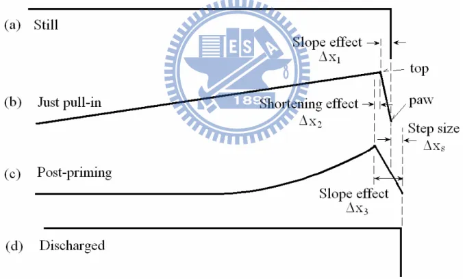
The operation of SDA from rest to scratch forward is classified into five states shown in
Figure 2-2. As the input voltage V increases from zero, the still SDA in Figure 2-2(a) starts
rotating about the bushing paw and the free edge of main beam just touches the dielectrics at the
pull-in voltage Vpi as in Figure 2-2(b). For input higher than pull-in voltage Vpi, the main beam
will be bent and gradually becomes a surface contact with the dielectrics as Figure 2-2(c),
so-called priming voltage Vpr. After that, the contact length of main beam to the dielectrics
increases as input voltage increases, it is so-called post-priming at voltage Vpp, as shown in
Figure 2-2(d). Finally, when the input voltage is fully discharged, the SDA will spring back and
keep the one forward step, as shown in Figure 2-2(e).
2.2 Static analysis of SDA
Some assumptions are made first before the derivation. The deformation and electrostatic
force are assumed to be same along the width direction of SDA, as the main plate may be treated by beam model [24]. The Euler-Bernoulli beam theory is applied on main plate and
support beams; the bushing, dielectrics and rails are assumed to be rigid. The angle between the
bushing and main plate remains right angle all over the deformation process, and the
electrostatic force acted on bushing is ignored. At pull-in, priming or post-priming state, the
contact between main beam and dielectrics remains. In other words, free end of main beam is
post-priming states. In static analysis, it is natural to draw the condition as no slippage occurs
during charging and discharging. The vertical displacement of bushing top is negligible during
main beam deflection in priming and post-priming states. The fringing effect of electrostatic
field is ignored.
For a general parallel plate capacitor, the distributed load q, i.e. the electrostatic force per
unit length applied to the plate, is given as
where ε0 is the permittivity of air; V is the input voltage; W is the plate width; d is the gap
between two plates. Let the SDA be modeled as plate capacitor, d is defined as the distance
from the main beam to the electrode on substrate, including air and the dielectric layers. The
distance d varies with the deflection y and electrostatic load q. Due to the nonlinear coupling
between the electrostatic load q and main beam deflection y, there is not yet an exact solution
for the deflection curve y. A square law of deflection has been proposed to define the deflection
curve of a cantilever beam under electrostatic force [8]. By combining Euler-Bernoulli beam
theory and the square law model, the governing equation of the main beam with the distributed
electrostatic load q(x) at post-priming state can be expressed as a fourth-order differential
equation:
where a is equal to the thickness t of the dielectric layer divided by the relative permittivity k; b
is equal to h / ln2; ln is the non-contact length of main beam at the given input voltage; h is the
bushing height; E is the Young’s modulus of SDA material; I is the second area moment of
main beam; x is the horizontal coordinate of the element in consideration. The downward 1) -(2 , 2 2 2 0 d WV q=ε 2) -(2 , ) ( ) ( d d 2 2 2 0 4 4 bx a EI WV EI x q x y + = = ε
deflection is defined as positive. The coordinate system is shown in Figure 2-3 where the origin
is defined at the juncture point between contact and non-contact regimes with distance h above.
Integrating equation (2-2) successively four times leads to following equations:
The four integration constants, c1, c2, c3, c4 and non-contact length ln, can be solved with the
following five boundary conditions:
Eq. (2-7) means the y position of origin remains to be the bushing height, h. Also, the contact
region is flat and fixed to the dielectrics at post-priming state, so the slope and moment at origin
O are zero, as implied by Eq. (2-8) and Eq. (2-9), respectively. Eq. (2-10) states that the vertical
displacement of bushing is negligible. Eq. (2-11) expresses the balance between the moment
EIy”(ln) of main beam and the torque kt y’(ln) from the support beam at x = ln. The parameter kt
is the torsional spring constant of support beam and defined as 2βGWpt3/Lp, where βis an
11) -(2 . ) ( ) ( 10) -(2 0 ) ( 9) -(2 0, (0) 8) -(2 0 (0) 7) -(2 (0) n n t n l EIy" l y' k , l y y" , y' h, y = = = = = 6) -(2 , 2 6 ) ) ( 12 ) ) ( ( tan ) 3 ( 24 4 ln 3 24 ) 1 ln( 2 ln 3 ( 5) -(2 , 2 ) ) ( 4 ) ) ( ( tan ) ( 4 ) 1 (ln ( d d 4) -(2 , c ) ) ( 2 ) ) ( ( tan 4 ln ( d d 3) -(2 , ) ) ( 2 ) ) ( ( tan ) ( 2 ( d d 4 3 2 2 3 1 2 3 2 1 1 3 2 2 2 2 2 0 3 2 2 1 2 3 2 1 1 2 2 0 2 1 2 1 2 1 1 2 0 2 2 1 2 1 2 1 1 2 2 0 3 3 c x c x c x c ab ab bx bx ax ab x a x b a bx a EI WV y c x c x c ab ab bx bx a ab a x EI WV x y x c ab a ab bx x ab a EI WV x y c ab a ab bx bx a a x EI WV x y + + + + + + − + + − = + + + + + − = + + + = + + + = − − − − ε ε ε ε
aspect ratio constant based on the ratio of the width to thickness of the support beam [25]; Wp is
the width of support beam; Lp is the length of support beam; G is shear modulus of SDA
material.
Applying the boundary condition of Eq. (2-7) to Eq. (2-9) into characteristic equations Eq.
(2-4) to Eq. (2-6), the integration constants c2, c3 and c4 can be solved as:
Applying Eq. (2-10) into characteristic Eq. (2-3), the integration constant c1 can be solved as:
Rewriting the expression of Eq. (2-11) in terms of Eq. (2-4) and Eq. (2-5) can lead to the
characteristic equation of non-contact length ln for given input V;
Since no explicit solution exists, the non-contact length ln is solved by numerical method. At the
priming state, the not-contact length is considered to be the same as the main beam length L,
and then the priming voltage Vpr can be determined from reorganizing Eq. (2-16) by replacing ln
with main beam length L as
15) -(2 . 6 ) 2 ) 1 ln( ) ( 2 ) ) ( ( tan ) 3 ( 1 ( 2 3 3 2 2 2 3 2 1 1 2 2 0 1 n n n n n n n l h l b a bl l ab ab bl bl a abl EI WV c − + + + − = − ε 14) -(2 . 8 ln 13) -(2 , 0 12) -(2 , 4 ln 2 4 2 0 4 3 2 0 2 ) h a l ( EI WV e h c c ab a EI WV c n − = = − = ε 16) -(2 }. 6 ] 2 ) 1 ln( 1 ) ( 2 ) ) ( ( tan 3 [ { } 3 ) 4 4 ) 1 ln( ) ( 4 ) ) ( ( tan 2 ( { 2 2 2 2 2 3 2 1 1 2 0 2 2 2 3 2 1 1 2 0 n n n n n n n n n n t l EIh l b a bl ab l ab ab bl a WV l h ab l l b a bl ab ab bl a EI WV k − + + + − = − + + + − − − ε ε
By definition, the bending moment M at any position x in non-contact part of main beam is
given by definition as following where flexural rigidity EI is constant
There are two methods to determine the position xmax where the maximum moment Mmax
happens along main beam for a specific input voltage. The first one is to decide the coordinate
that the shear force, −EI( dy/dx), becomes zero. Then substituting this coordinate into Eq. (2-20) will find the maximum moment. The one is straight forward in applying the optimization
toolbox in Matlab to find out the extreme value along main beam. The maximum bending stress
σmax along main beam for corresponding input can be expressed as:
The horizontal output force Fo of charged SDA array along the main beam varies with the
input voltage. The friction force along contact regime is assumed to be large enough to keep the
contact area stationary. The horizontal output force Fo is basically the horizontal component of
21) -(2 6 2 max max Wt M s = 20) -(2 . 6 ] 2 ) 1 ln( ) ( 2 ) ) ( ( tan 3 )) ) ( ( tan ) ) ( ( tan ( [ d d 3 3 2 2 2 2 3 2 2 1 1 2 1 1 2 1 1 2 2 0 2 2 x l EIh l b a bl x abl x l ab ab bl ax ab bl ab bx x bl WV x y EI M n n n n n n n n + + − − + + − = − = − − − ε 19) -(2 . 2 1 ln 1 2 tan 3 18) -(2 , 4 4 1 ln 4 tan 2 17) -(2 where , ] 6 3 [ 2 2 2 2 3 2 1 1 0 2 2 2 3 2 1 1 0 1 2 1 2 1 2 ) L b ) a bL ( ab L (ab) ) (ab) bL ( a W( e A ) ab L bL ) a bL ( (ab) )) (ab) bL ( a ( EI W k e A A A ) L EIh L h k ( V t t pr + + + − = + + + − = − − = − −
the electrostatic force along main beam. It can be solved by integrating the horizontal
component of electrostatic force along the non-contact part as:
where N is the SDA number in the SDA array, θ is the angle between the horizontal and the tangent line along main beam, and can be calculated from the slope of deflection curve.
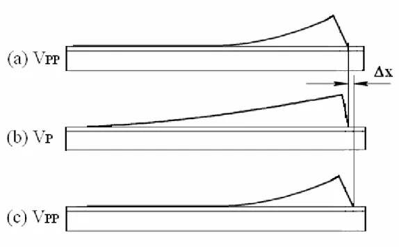
In order to recognize SDA step size in fully discharge mode, Figure 2-4 shows the SDA
deflection and displacement of bushing from still, charge and discharge. At pull-in voltage, the
SDA rotates about bushing paw. Due to the slope change on bushing, the bushing top moves
back horizontally with magnitude △x1=h*sin(tan−1(h/L)), as shown in Figure 2-4(a). When the
input voltage is equal to or larger than the priming voltage, the main beam starts bending and
causes the bushing top to move backward more due to so-called curvature shortening effect,
which has not been considered in previous literatures on SDA. The lateral displacement due to
curvature shortening effect can be formulated as △x2= dx
x y n l
∫
0 2 ) d d ( 2 1 in Figure 2-4(b) [25].This effect will make the bushing rotate more in counterclockwise, and then the bushing paw
moves forward for certain horizontal distance given by △x3=h*|dy/dx|as shown in Figure
2-4(c). When SDA is fully discharged, the main beam will spring back and rotate about the
bushing paw as Figure 2-4(d). By combining the net effect of three above effects, the step size
in this type of SDA motion control becomes
The weakness of driving method in Figure 2-4 is that the main beam may rotate too much.
As a result, SDA is possible to turn over or not easy to pull back by electrostatic force 23) -(2 ) d d ( 2 1 )) sin(tan d d ( * x -x -x x 0 2 1 2 1 3 dx x y L h x y h ln bushing
∫
− − = ∆ ∆ ∆ = ∆ − 22) -(2 , ) ( sin 0 2 2 2 0∫
+ = ln o dx bx a WV N F ε θimmediately. An effective alternate driving method is to keep the main beam constantly contact
with dielectrics under input levels VP and VPP between priming and some post-priming input.
Figure 2-5 shows the components of step size in this driving mode, i.e., constantly contact mode.
As the slope effect ∆x1 is avoided, the net step size ∆x may be simplified as
the step size at input voltage VPP, ∆xpp minus the step size at input voltage VP , ∆xp.
24) -(2 x x x=∆ PP−∆ P ∆
2.3 Dynamic analysis of SDA
To explore the dynamic behavior of SDA including friction effect, a mass-spring-damper
model of single degree of freedom (SDOF) is proposed as an approximation. The equation of
motion and its normalized form are given as Eq. (2-25) and Eq. (2-26)
The coordinate x and its first and second derivatives of with respect to time are the displacement,
velocity and acceleration of SDA, respectively. The lump-mass m defines the total mass of
SDA array including the ring around SDA. The coefficient k defines the spring constant of the
suspended tether spring. The damper may contain one or two types of friction; the first is
viscous damping of coefficient c of contact surface between main beam and insulated layer.
The second one is the Coulomb friction of coefficient µ accounting for the stick-slip phenomenon in contact surfaces. The force FN is the normal force between the contact area of
main beam and insulated layer. In MEMS, the body force such as gravity force is often much
less than surface traction force as the electrostatic force. So the normal force is simplified to
contain only the electrostatic force in the contact area. The force FO is the amplitude of driving
force which is the resultant horizontal component of the electrostatic force applied along the
main beam of SDA, the force along bushing is ignored here. The driving voltage is in sinusoidal
wave sin(ωt) of angular velocity ω. However, it should be noted that the electrostatic force is an attractive force between contact surfaces, no matter the charge on main beam is positive or
negative. Therefore, the driving force is expressed as the absolute value of driving voltage
waveform, i.e., abs(sin(ωt)) multiplying FO, which is the motive force that makes SDA scratch
forward. The friction terms in Eq. (2-25) may be and rearranged as following
26) -(2 )) (sin( * ) ( 25) -(2 )) (sin( * ) ( t abs m F x m k x sign m F x m c x t abs F kx x sign F x c x m O N O N ω µ ω µ = + + + = + + + & & & & & & & &
In Eq. (2-27), sign(~) is the sign function result of the operand in parenthesis; the gain (c/m) is
defined as a regulation factor that modifies viscous friction coefficient. The offset (µFN/m) is
the dry friction force that should be overcome in motion. To simplify the derivation, the static
and dynamic dry friction coefficients are assumed to be same as µ.
When the Coulomb friction is activated, the analysis of displacement (total travel distance)
response is too complex to derive an exact and compact analytical solution. To solve this type
of nonlinear vibration problems, some methods have been developed such as perturbation
method, averaging method, multiple scales method and direct separation of motions [26-30].
Instead of these methods, direct numerical simulation method as Simulink in Matlab has been adopted to investigate the dynamic response in a straight forward way to simulate the
dynamical behavior of SDA.
To evaluate the fatigue behavior of SDA, the information of stress bounds are needed. Eq.
(2-21) may calculate the maximum and minimum stresses as following
The equivalent stress σR, the fully reverse stress of same fatigue life [31], is expressed as
The minimum moment Mmin at specific input, though not easily be derived, lies between zero
for fully discharge mode and the maximum moment at Vp in constantly contact mode. 27) -(2 ) ) ( * ( * ) ( ) (
sign x sign x gain abs x offset
m F x m c N + =
+ & & &
& µ 28) -(2 6 , 6 2 min min 2 max max Wt M s Wt M s = = 30) -(2 . 2 , 2 where 29) -(2 min max r min max av r e ult av R σ σ σ σ σ σ σ σ − = + = + = s s s
Figure 2-1. Structures and elements of SDA. (a) Support beams are free at contact part.
(b) contact part is constrained to slide without rotation [24].
substrate
dielectrics
rail
main plate
bushing
support beam
W
L
W
pL
pt
h
(a)
(b)
Figure 2-2. Five states in SDA operation at different input voltages: (a) initial, zero
input; (b) pull-in, voltage Vpi; (c) priming, voltage Vpr; (d) post-priming, voltage Vpp;
Figure 2-3. Coordinate system and electrostatic force density in post-priming
configuration. The electrostatic force density in contact region is constant. In non-contact region, the electrostatic force density follows Petersen model [8].
Figure 2-4. Step size of SDA operated in fully-discharge mode. (a) Initial state. (b)
The main plate rotates around bushing paw and causes lateral backward movement ∆x1. (c) The curvature shortening effect causes the bushing top lateral movement
∆x2 backward more. Also, the bushing paw displaces ∆x3 forward. (d) SDA is
Figure 2-5. Step size of SDA operated in constantly-contact mode. (a) Initial state
at voltage VPP. (b) Partly discharge to voltage VP , main plate springs back. (c)
Chapter 3
Performance Enhancement of Scratch Drive
Actuator with Modified Flexible Joint
3.1 Concept design of low voltage Scratch Drive Actuator (LVSDA)
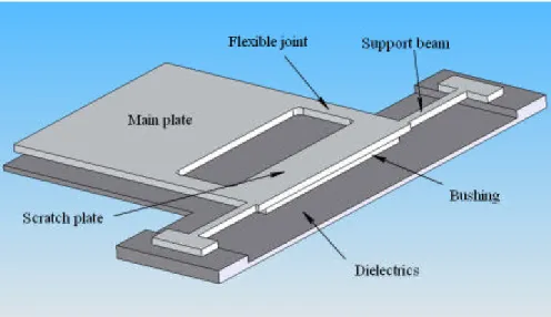
The concept design of the proposed LVSDA is shown in Figure 3-1, where two narrow
beams as flexible joint are placed between the main plate and scratch plate. The operation
procedures of LVSDA and conventional SDA are illustrated in Figure 3-2. They are both at rest
initially with zero input in Figure 3-2(a). When the input increases to snap-through voltage, the
free edge of main plate of LVSDA or SDA will touch the dielectrics (Figure 3-2(b)). At the
same input voltage, LVSDA will snap through more due to the smaller flexural rigidity to
generate a larger bushing lateral displacement, as shown in Figure 3-2(b). At an even higher
input voltage, the main plate will contact with the dielectrics more area and further push the
bushing forward, as Figure 3-2(c). After discharging, LVSDA or SDA will bounce back to
complete one cycle with one forward step size ∆x, as Figure 3-2(d).
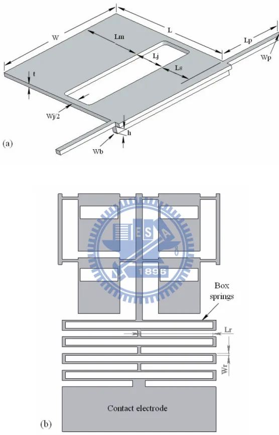
In order to fabricate and test the proposed LVSDA, the geometric parameters in LVSDA
are defined in Figure 3-3(a). The design of testing device is illustrated in Figure 3-3(b), where a
tether spring consisted of four box springs links four LVSDAs to the contact electrode. The
comparison between the proposed LVSDA and conventional SDA is based on the same device
size. It means all LVSDAs and SDAs here have the same total plate length L and plate width W,
which are fixed as 80 µm and 65 µm, respectively.
L will remain to be 80 µm, as well as the plate length of SDA. The thickness t of plate, spring, and support beams, as well as the bushing height, of LVSDA and SDA is all set at 2 µm. Each support beam has length Lp= 25 µm and width Wp= 3 µm. Different flexible joint
dimensions and locations are designed to investigate their effects on performance. A shorter or
wider flexible joint will provide a more rigid joint. Two different flexible joint widths Wj are
designed as 6 µm and 12 µm. The designed flexible joint length Lj includes 15 µm and 20 µm.
The designed scratch plate length Ls includes 10 µm, 15 µm, and 20 µm. A shorter Ls means the
flexible joint is closer to the bushing.Due to different combinations on scratch plate length and
flexible joint length, the corresponding main plate length Lm of LVSDA includes 50 µm, 45 µm
and 40 µm to keep the total plate length as 80 µm. The designed LVSDA dimensions are denoted as LV-Ls-Lj-Lm-Wj. For example, the test device expressed as LV-10-20-50-12 has
following dimensions: Ls=10 µm, Lj=20 µm, Lm=50 µm, and Wj=12 µm. Eight types of LVSDA
used in this work are listed in Table 3-1.
The spring constant of one box spring can be expressed as [24]:
k1=EtWr3/(Lr3), (3-1)
where E is the Young’s modulus of spring material, t and Wr are the thickness and width of
spring beam, respectively, and Lr is the half length of box spring. For the tether spring
composed of 4 box springs, the equivalent spring constant becomes
k = EtWr3/(4Lr3), (3-2)
The output force of LVSDA or SDA can be determined from the result of spring constant
multiplied by the deflection of spring.
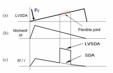
3.2 Qualitative Analysis of LVSDA
In order to analyze the deflection of LVSDA under given input, a detailed free body
diagram for input between snap-through and priming is plotted in Figure 3-4. The equivalent
decrease or the moment should increase. As the increasing of moment needs increasing the
input which violates the purpose of low-voltage, the reasonable way is to reduce the flexural
rigidity EI of the device. By decreasing EI, the LVSDA can be deflected to provide certain
force at lower voltage than SDA. In other words, the electrostatic force to resist the mechanical
force can be reduced.
3.3 Finite element analysis of LVSDA
The finite element analysis is realized by SolidWorks® and CosmosWorks®. The behavior
of LVSDA has been analyzed in detail and will be compared with the experimental results. For
stress simulations, since plastic deformation may happen in flexible joint at high driving
voltage, the finite element analysis (FEA) in this work are performed by elasto-plastic model in
nonlinear static analysis package of CosmosWorks. According to the material properties of micro electroplated nickel [26-29], the Young’s modulus E is selected as 171 GPa, yielding
stress is 323 MPa and tangent modulus in plastic region is assigned as 17.1 MPa. The fatigue
stress is 195 MPa, and the ultimate stress is 560 MPa. Parameters used in FEA are listed in
Table 3-2. The solid modeling process is first to sketch the main body of LVSDA and substrate
separately, combining them as assembly with suitable conditions. Then apply material
properties to each part; assign constraints according to requirements; apply electrostatic
pressure and external load, the pressure is specific for every input voltage. Assign contact
conditions on faces that may contact each other during loading, the no-penetration condition is
the most important setting to make sure the LVSDA will not penetrate into the ground layer.
The meshing size of element often uses default value or even finer value; the results always
converge at about 1.0e-3 level. The friction coefficient between contact surfaces is set as 0.2 in
The electrostatic force on scratch plate, flexible joint, support beams and bushing are
neglected. The left edge of main plate is set to be pinned with the dielectric layer and no
penetration is allowed. The electrostatic pressure for a given input voltage is approximated by
the parallel capacitor model for each strip of 2.5 µm along the main plate. Then stress in the test structure and the contact length between main plate surface and dielectric layer at different
input voltages can be simulated. In simulations, the input voltage starts from 40 volts to 120
volts with increment of 10 volts, since all measured threshold voltages are at least 40 volts. A
typical simulated result from the CosmosWorks is shown in Figure 3-5 for device
LV-20-20-40-6 at 70 volts. It is found that the maximum stress happens around flexible joint
corner next to the main plate and exceeds the yielding stress (Figure 3-5(a)). The contact length
between the main plate and dielectric layer is about 20 µm (Figure 3-5(b)). The fully-discharge shape is shown in Figure 3-5(c), in which permanent vertical displacement due to plastic
Figure 3-1. Concept design of low-voltage Scratch Drive Actuator (LVSDA) with
flexible joint.
Figure 3-2. Operation procedures of conventional SDA and LVSDA: (a) at rest
initially; (b) snap-through ;(c) contact more at higher input voltage; (d) discharge and complete one step size ahead.
Figure 3-3. Design layout of micro-electroplated nickel SDA. (a) Definition of LVSDA
geometric parameters. In another word, the sum of main plate length Lm, flexible joint
length Lj and scratch plate length. (b) Four LVSDAs with tether spring connected to the
Figure 3-4. Qualitative analysis on flexible joint effect. (a) Equivalent electrostatic
force is FE . (b) Moment M along device similar to SDA. (c) ( M/I ) ratio changes
hugely along flexible joint in LVSDA. So, the flexible joint reduces flexural rigidity, increases bending stress, induces more deflection and makes LVSDA easier output at lower voltage.
Figure 3-5. Finite Element Analysis (FEA) results of LVSDA with Ls=20, Lj=20,
Lm=40 and Wj=6 µm ( LV-20-20-40-6) at 70 V. (a) Stress distribution, where the maximum von-Mises stress happens at the flexible joint corners close to the main plate. (b) Side view at maximum loading, contact length is about 20 µm. (c) Side view after loading is fully-relax, contact length is about 2 µm. The permanent vertical deflection UY shows plastic deformation at left side on flexible joint that will affect the LVSDA output performance hereafter.
Table 3-1. Notation of LVSDA testing types Notation LV-Ls-Lj-Lm-Wj Ls (µm) Scratch Plate Length Lj (µm) Flexible Joint Length Lm (µm) Main Plate Length Wj (µm) Flexible Joint Width LV-10-20-50-6 10 20 50 6 LV-10-20-50-12 10 20 50 12 LV-15-15-50-6 15 15 50 6 LV-15-15-50-12 15 15 50 12 LV-15-20-45-6 15 20 45 6 LV-15-20-45-12 15 20 45 12 LV-20-20-40-6 20 20 40 6 LV-20-20-40-12 20 20 40 12
Table 3-2. Simulation parameters for FEA
Parameters magnitude Parameters magnitude
Total main plate length, L, µm 80 Support beam width, Wp, µm 3
Scratch plate length, Ls, µm 10, 15, 20 Plate thickness for all, t,µm 2
Flexible joint length, Lj, µm 15, 20 Bushing height, h, µm 2
Main plate length, Lm, µm 40, 45, 50 Bushing width, Wb, µm 3
Main plate width, W , µm 65 Box spring length, Lr, µm 110
Flexible joint width, Wj, µm 6, 12 Spring beam width, Wr, µm 3
Support beam length, Lp, µm 25 Young’s modulus of nickel , E, 171
Spring thickness, same as t, 2 Shear modulus, G, GPa 69 Tether spring constant, 1.98 Yielding stress, σy, MPa 323
Tangent modulus, σt, MPa 17.1 Element size, µm 2.5
Total nodes 26220 Total elements 15525
Note: The structure material, microelectroplated nickel, is defined as isotropic hardening of
von-Mises plasticity once yielding. The solver use sparse matrix of Newton-Raphson
Chapter 4 Fabrication and Results
In order to verify the validity of the proposed models of SDA and LVSDA, a two-mask
micro-electroplated nickel surface-micromachining process is chosen to construct Ni SDA and
LVSDA array structures. The test structure is composed of four SDAs or LVSDAs connected to
a suspended spring which is anchored to the contact electrode.
4.1 Fabrication process
The fabrication process is summarized as following: (a) Starting from a 4-in. RCA-clean
(100) wafer, a 6000Å thick LPCVD silicon nitride is grown in furnace as the dielectric layer
(Figure 4-1(a)). (b) First patterning process: coating 2µm photoresist FH6400 as sacrificial
layer, 90℃ soft bake 10 minutes, hydration reaction 20 minutes, then creating the pattern of
bushing and contact electrode by the first mask (Figure 4-1(b)). (c) Sputtering process: 200Å
thick Ti and 1500Å thick Cu are sputtered sequentially as the adhesive layer and seed layer,
respectively (Figure 4-1(c)). (d) Second patterning process: coating 5µm thick photoresist
AZ9260, then creating the pattern of electroplating mold by the second mask (Figure 4-1(d)).
(e) Electroplating nickel process: electroplating the Ni test structure with Watt bath with
current density 10 mA/cm2 over 10 minutes to form 2µm thick Ni (Figure 4-1(e)). (f) Release
process: using Acetone to remove electroplating mold AZ9260, then removing Cu seed layer
by CR-7T solution about 20 seconds. Ti adhesive layer is then removed by BOE solution
about 10 seconds, then the removal of FH6400 sacrificial layer by Acetone for 30 minutes. By
immersing in IPA solution and vibrating about 20 seconds for releasing, then drying at 60℃, a
fully suspended test Ni structure can be obtained as in Figure 4-1(f). Typical fabricated results
bushing, and (d) close-view of LVSDA. The lithography parameters are listed I Table 4-1;
while the electroplating parameters are listed in Table 4-2 for reference.
The experimental equipments for loading test include an optical microscope mounted with a
CCD camera, PC with image process software, chip position table, function generator,
high-voltage power amplifier and probe station. The test chip is fixed on the position table by
vacuum chuck. Two probes are adjusted to touch the contact electrode of SDA array and
substrate. The test signal is generated from the function generator, amplified and calibrated by
the high-voltage power amplifier in sinusoidal waveform of 500 Hz. This input is composed of
a DC offset at 30 volts often and AC voltage depending on the control command. For example,
when the driving signal needs to vary in the range of 30 to 120 volts, the chosen DC offset is 30
volts and AC amplitude is 90 volts in peak to peak definition. The motion of SDA or LVSDA
array is recorded by the CCD in computer and then analyzed by using image process software.
Typical measurement set-up and driving test are shown in Figure 4-3.
Figure 4-1. Fabrication process of micro-electroplated nickel SDA. (a) LPCVD Si3N4,
(b) bushing and fixture patterning, (c) Cu/Ti seed layer, (d) device structure patterning, (e) nickel electroplating, (f) release.
(a)
(b)
(c)
(d)
(e)
(f)
Table 4-1. Lithography parameters Photoresist FH6400 AZ9260 Thickness 2.1 µm 5 µm Spinning 500 rpm (10 sec) 1200 rpm (25 sec) 1000 rpm (10 sec) 5000 rpm (30 sec)
Waiting 5 min 10min
Soft Bake 2 min 10 min
Hydration 5 min > 20 min
Exposure 3 sec (+20%) (46mW/cm2) 6 sec (+20%) (46mW/cm2)
Develop 30 sec (AZ-400k) 2 min 30 sec (AZ-400k)
Fix 1 min (DI Water) 1 min (DI Water)
Hard Bake 10 min X
Table 4-2. Electroplating parameters
Mask Mask #2
Metal Nickel
Area 3.526 cm2
Current Density 10 mA/cm2
Figure 4-3. Driving test of released devices. (a) Measurement set-up, and (b) driving
test of SDA array.
Figure 4-2. SEM pictures of fabricated results. (a) Top view of SDA array; (b) Top view
4.2 Analytical and testing results of SDA
In this subsection, the simulated and numerical results of SDA model developed in chapter
2 will be presented and compared with testing results of Ni SDA of 80 µm long and 65µm wide. Some discussions will be made on the key factors of SDA performance.
4.2.1 Static analytical results of SDA
Numerical codes on Matlab software are developed to perform the deflection analysis on the first proposed model based on parameters listed in Table 1. The non-contact length ln is
calculated first from Eq. (2-16) at each specified input voltage from 40 to 120 volts with
increment in 10 volts. The results are plotted in Figure 4-4 where the non-contact length in this
work is shorter than that of Kazuaki’s work. As the simulation of electrostatic force in this work
is better than Kazuaki’s work, the chosen size of SDA may be smaller and save the chip size.
The priming voltage Vpr of the device is calculated from Eq. (2-17) as shown in Figure 4-5. All
models, including this work, Linderman’s and Kazuaki’s works, how that shorter plate needs
higher priming voltage to maintain the contact between main plate and dielectrics. This work
still shows smaller priming voltage than that of the other two models for same plate length. The
step size for different control method out of Eq. (2-23) and Eq. (2-24) are plotted in Figure 4-6.
The step sizes in fully-discharged mode of this work and Kazuaki’s work have been shown in
Figure 4-6(a). As the main plate tends to turn over at the end of discharge, the SDA operation is
not stable enough. Consequently, constantly-contact mode is a stable way for SDA operation as
shown in Figure 2-5. The SDA is driven between two input levels which are all equal to or
larger than priming voltage, and the main plate always keeps contact with dielectrics during
charge and discharge cycles. The step size in this mode is the step size at maximum input minus
the step size at minimum input. Figure 4-6(b) shows the results when priming voltage is the
In Figure 4-7(a), the first reported bending moment diagrams of SDA are shown based on
Eq. (2-20). The bending moment is zero over the entire contact part and at the starting point of
non-contact part. Then it increases rapidly to maximum; after that, it goes down to the local
minimum at the right end. The value of maximum moment and where it happens depends on the
input level. From the trajectory of maximum moment Mm, it is obvious that Mm becomes higher
and shifts rightward as input increases. The maximum static bending stress σm along main plate
for different input is plotted in Figure 4-7(b). This maximum stress, calculated by Eq. (2-21) as
from 182 to 495 MPa for input voltages from 40 volts to 120 volts, also locates at same place of
maximum moment for same input voltage.
Some mechanical properties of micro-fabricated Nickel useful in this work are adopted
from literature; the Young’s modulus of Nickel is chosen as 171 MPa; the yield strength is
chosen as 323 MPa [32, 33]; the ultimate strength is chosen as 560 MPa [34, 38]. As the fatigue
strength, [29] reported a value of 195 MPa for one million life cycles and constructed the S-N
curve of Nickel under cyclic reverse loading test. For the driving test in continuously
charge/discharge, the suitable failure mode is fatigue instead of yielding stress for static load.
This topic will be discussed in subsection 4.2.2.
4.2.2 Dynamic analytical results of SDA
As some devices fail at higher voltage, it is proper to adopt the fatigue design theory [30] for
cyclic loading to explore the cause. For a fully reversal loading with zero average stress, the
stress amplitude σR and the device life cycles N is related by the Basquin’s equation,
where the coefficients A and B can be determined from the fatigue test data. For a non-fully
reversal loading with stress amplitude σr and average stress σav not being zero, it is readily to
decide the equivalent stress amplitude σ by the Goodman’s equation, σ =σ +σ σ/σ ,
1) -(4 , log * log logA= σR +B N
![Figure 1-1. Operation principles of SDA [1]. (a) Terminologies, (b) SDA placed on insulator and substrate, driven by voltage pulse in capacitor circuit, (c) Positive signal, main plate priming, bushing scratches ahead, (d) Low signal, main plate spri](https://thumb-ap.123doks.com/thumbv2/9libinfo/8485153.184380/19.892.273.621.120.716/operation-principles-terminologies-insulator-substrate-capacitor-positive-scratches.webp)
![Figure 1-4. Step size estimated from experimental results in Langlet’s work [19].](https://thumb-ap.123doks.com/thumbv2/9libinfo/8485153.184380/21.892.185.695.133.284/figure-step-size-estimated-experimental-results-langlet-work.webp)