行政院國家科學委員會專題研究計畫 成果報告
旋塗式有機薄膜電晶體的電性研究與製程開發(I)
計畫類別: 個別型計畫 計畫編號: NSC94-2215-E-009-075- 執行期間: 94 年 08 月 01 日至 95 年 07 月 31 日 執行單位: 國立交通大學電子工程學系及電子研究所 計畫主持人: 羅正忠 計畫參與人員: 陳世璋,倪佳寧,紀伯翰,傅文煜,呂國源 報告類型: 精簡報告 處理方式: 本計畫可公開查詢中 華 民 國 95 年 8 月 1 日
行政院國家科學委員會補助專題研究計畫
■成果報告
□期中進度報告
旋塗式有機薄膜電晶體的電性研究與製程開發(I)
計畫類別:■ 個別型計畫 □ 整合型計畫
計畫編號:NSC 94-2215-E-009-075
執行期間:94 年 08 月 01 日至 95 年 07 月 31 日
計畫主持人:羅正忠
計畫參與人員: 陳世璋,倪佳寧,紀伯翰,傅文煜,呂國源。
成果報告類型(依經費核定清單規定繳交):■精簡報告 □完整報告
本成果報告包括以下應繳交之附件:
□赴國外出差或研習心得報告一份
□赴大陸地區出差或研習心得報告一份
□出席國際學術會議心得報告及發表之論文各一份
□國際合作研究計畫國外研究報告書一份
處理方式:除產學合作研究計畫、提升產業技術及人才培育研究計畫、
列管計畫及下列情形者外,得立即公開查詢
□涉及專利或其他智慧財產權,□一年□二年後可公開查詢
執行單位: 交通大學電子工程研究所
中 華 民 國 95 年 07 月 23 日
中文摘要 旋塗式有機薄膜電晶體有利於大面積且低成本的元件製作。本計畫的研究目標為評估 製造旋塗式有機薄膜電晶體的可行性。在本計畫中,我們致力於P3HT 的電特性討論,製 程的研究以及有機薄膜電晶體的電特性探討。P3HT 是一種半結晶的物質,用 P3HT 所做成 的薄膜電晶體其載子移動率(mobility)受制於非結晶區域。從電晶體的電特性測量中,我們 發現元件受到氧氣的作用,使得電晶體的臨界電壓(threshold voltage)與有機薄膜的導電性 (conductivity)會增加。我們從有著 Ni 金屬電擊和 top-contact 結構的電晶體中得到了最佳的 元件載子移動率,探討其原因,是由於較好的晶體結構與較低的金屬電擊接觸電阻(contact resistance)所造成。此外我們發現載子移動率會隨溫度升高而增加,這證實了載子在 P3HT 中可以藉由hopping 的載子傳導機制來解釋。我們也發現沒有保護層的薄膜電晶體其電特 性會隨時間的增加而產生劣化。在實驗中我們發現旋塗式的有機薄膜需要定義(pattern)以隔 離元件,否則元件的絕緣層會因為有機層的污染而造成不必要的漏電產生,如此一來元件 的電特性會跟著變差。 Abstract
Organic thin film transistors made by Spin-Coating method with solution processable conjugated polymers have potential advantages for fabricating low-cost, large area devices. The goal of this project was to evaluate the feasibility of Spin-Coating method in fabricating organic thin film transistor with solution processable conjugated polymers. In this thesis, we emphasize the electrical characteristics of poly-3-hexylthiophene (P3HT), investigation of spin-coating process parameters and the electrical characteristics of OTFT with P3HT active layer. P3HT is semi-crystalline; the mobility is limited by amorphous part of P3HT. We have measured conductance, mobility, and ON-OFF current ratio of OTFTs. The best mobility of P3HT OTFT was obtained with a top-contact structure with Ni S/D contacts as a result of a good P3HT molecular morphology and low S/D contact resistance. And we found that the mobility is thermal activated (an evidence for hopping transport mechanism). In addition we found that the conductivity of P3HT film and threshold voltage of OTFT increases when the oxygen molecular is interacted with the P3HT film. A degradation of OTFT without a passivation layer was observed. For a good OTFT performance the organic active layer is needed to be patterned to reduce the gate leakage current.
Introduction
Organic semiconductors are emerging as competitors to amorphous and polycrystalline silicon in the application of large area electronics. Particular emphasis has been placed on conjugated polymer semiconductors. This is due to the ease of solution processing of the polymer compared with gaseous deposition of amorphous silicon.
Organic thin film transistors (OTFTs) based on conjugated polymers or oligomers have been envisioned as a viable alternative to more traditional, mainstream thin film transistors (TFTs) based on inorganic materials. Because of the relatively low mobility of organic semiconductors, OTFTs cannot rival the performance of field-effect transistors based on single-crystalline inorganic semiconductors, such as Si, Ge, and GaAs. However, the unique processing
characteristics and demonstrated performance of OTFTs suggest that they can be competitive candidates for existing or novel thin film transistor applications requiring large area coverage, structural flexibility, low temperature processing, and especially low cost. Progress in performance of p-type organic thin film transistors is shown in table 1 [1].
Solution-processable conjugated polymers are among the most promising candidates for a cheap electronic and optoelectronic technology on plastic substrates. The technology that is believed to have the potential to produce the highest impact on manufacturing costs is the use of soluble organic semiconductors, both polymers and oligomers, combined with large area coating or that could eliminate lithograph. One of the appealing aspects of most of the organic materials employed in OTFTs is the fact that they can be deposited using very low cost procedures such as spin-coating. This is the case of soluble polymers such as regioregular polythiophenes we used in experiments. Spin-coating procedures are also thermally compatible with plastic substrates, because they are carried out at room temperature. To study the feasibility of Spin-coating technology with solution processable conjugated polymers, further investigation is required. Here, we employ the poly-3-hexylthiophene (P3HT), solution processable conjugated materials, as active layers in OTFTs.
I. Property of P3HT and Spin-Coating Technique 1.Introduction
One of the first solution-processable organic semiconductors used for FETs was poly-3-hexylthiophene or P3HT, in which the addition of alkyl side-chains enhanced the solubility of the polymer chains [2]. The morphology of P3HT can be very different dependent on the purity of P3HT and solvents, deposition method, process condition and environment condition. Of course the electrical characteristics of P3HT OTFT can be very different with different molecular morphology. A detail understanding the property of molecular polymer and the transport mechanism is required in order to get a better performance of OTFT. So study of research papers is needed for a successful experiment. In this paper, data relevant to P3HT will be presented.
The differences among deposition methods will be discussed to emphasize the advantage of solution processes, especially the spin-coating method. Some process parameters about spin-coating will be discussed in this chapter.
2. The Characteristics of P3HT 2-1. The Molecular Structure of P3HT
The structure of the polymer chain of P3HT is shown in Fig. 1.1. The 3-alkyl substituents can be incorporated into a polymer chain with two different regioregularities: head to tail (HT) and head to head (HH) [3].
R represents the alkyl side chain (C6H13, for hexylthiophene), which allows them to be dissolved
in solvents like chloroform. This solution processability enables simple film deposition, one of the major attractions of conjugated polymers. A regiorandom P3HT consists of both HH and HT 3-hexyllthiophenes in a random pattern while a regioregular P3AT has only one kind of 3-alkylthiophene, either HH or HT. The position and direction of the side chain in the diagram
shows a very highly ordered system. This type of order is known as regioregularity and has been shown to give much higher field-effect mobility values over regiorandom (disordered side chains) material [4]. Most interestingly, these polymers have been shown to have very different properties from their corresponding regiorandom polymers, such as smaller band gaps, better ordering and crystallinity in their solid states, and substantially improved electroconductivities. When regioregular P3HT consisting of 98.5% or more head-to-tail (HT) linkages was used to fabricate FETs, a dramatic increase in mobility was observed relative to regiorandom poly-3-alkylthiophenes [5].
2-2. Effect of Polymer Morphology and Solvents
The molecular structure of the P3HT greatly influences the charge carrier mobility and
related current–voltage (I-V) characteristics of OTFTs. A comparison study of P3ATs (A = hexyl, octyl, dodecyl, hexadecy) with side chains ranging in length from butyl to decyl showed that field-effect mobility decreases with increasing chain length [6].
Under different processing conditions, the field effect mobility of OTFTs is highly anisotropic. For example, Karl et al [7] observed that the field effect mobility was highly anisotropic, with the larger mobility along the direction in which the polymer chain axis aligned.
The molecular structure obtained by using spin-coating method is different to the one by using solution-cast method. The mobility of spin-coated films is usually lower than that of the cast films [5]. This is perhaps because in the cast films, the rate of solvent evaporation is slower and has slower crystal growth, and hence betters ordering, and larger grain size.
The choice of solvents and polymers has a very significant impact on the electrical characteristics of OTFTs. In a recent publication, Bao et al. [8] observed that when chloroform was used as a solvent to make poly- (3-hexylthiophene)-based transistors, the field-effect mobility was 0.1 cm2/Vs. However when Tetra hydrofuran (THF) was used as the solvent, the value of field-effect mobility is only 0.0006 cm2/Vs. Table 2-1 shows the performance of various devices made from casting poly(3-hexylthiophene) films using different solvents with different process conditions.[8].
Sirringhaus et al., [9] observed that the mobility could differ by a factor of 100 depending on the orientation of the lamella structure of the polymer films. The mobility is highest along the direction of π-π stacking in which efficient inter-chain transport is happened.
The polymer solution we used is regioregular P3HT in xylene with high purity. From table
2-1, the mobility is typically in the range of 10-3 cm2/Vs which matches the result obtained in our experiment.
2-3. Charge transport through the P3HT
As in traditional inorganic semi-conductors, organic materials can function either as p-type or n-type. In p-type semi-conductors the majority carriers are holes, and this is the case of P3HT. Charge transfer occurs along the backbone of the chain through the system of alternating double and single bonds between carbon atoms. This alternating system gives rise to a separation of the bonding and anti-bonding states resulting in the formation of a forbidden energy gap. Anti-bonding states form the conduction band, as they are higher in energy and bonding states form the valence band being lower in energy.
The one-dimensional nature of the polymer chain means that separation of generated electron–hole pairs is difficult. Therefore, inversion of the polymer is not possible and field-effect devices operate in accumulation mode.
P3HT are semi-crystalline in nature, and their conduction mechanism is complex. The crystalline portion can conduct current through intra-chain and inter-chain transport, whereas the amorphous portion conducts current through hopping processes [9].
3 Spin-Coating technique
3-1. Conventional methods of OTFT fabrication
Three methods have been used to fabricate organic TFT devices. In the first method, a semi-conducting polymer layer is formed directly on the electrodes by electrochemical polymerization, and these electrodes are used subsequently as drain and source electrodes. The second technique utilizes vacuum deposition of oligomers and organic materials of low molecular weights. The third technique involves the use of a soluble material, either a conjugated polymer such as poly-3-alkylthiophene (P3AT) or precursor materials that can undergo subsequent chemical reactions to give the desired compounds. In our experiment we used the solution-processed method to fabricate OTFTs.
3-2. The need for Spin-coat technique
The organic semiconductors that exhibit the best mobility, ON/OFF current ratio, uniformity over large areas, and device reproducibility have been deposited by vacuum sublimation. However the need for expensive vacuum chambers and lengthy pump-down cycles is unavoidable.
Since the organic semiconductors have the relatively low mobility of organic semiconductors as described in chapter 1, OTFTs cannot rival the performance of field-effect transistors based on single-crystalline inorganic semiconductors, such as Si, Ge, and GaAs. However, the unique processing characteristics and demonstrated performance of OTFTs suggest that they can be competitive candidates for existing or novel thin film transistor applications requiring large area coverage, structural flexibility, low temperature processing, and especially low cost. Some recent efforts in this field have focused on processes for solution deposition of small molecules [10] and polymers, as well as integration of these processes with other non-lithographic device fabrication techniques [11]. To truly realize the advantages (i.e., processability and low cost) of organic materials in device applications, liquid phase processing technique by spin-coating is strongly desired. In all of our experiments, we used spin-coating technique as a key process of organic layer fabrication.
3-3. The Relationship between Spin-Speed and Film Thickness 3-3-1 Film Thickness Measurement by N&K Analyzer
Experiments
We prepared P3HT thin film with different spin-speed, and then measured film thickness by N&K analyzer to study the relationship between film thickness and spin speed. At first an n-type bare silicon wafer was cleaned by standard RCA cleaning process. Afterward, 1000Å thermal oxide was formed on silicon wafer. P3HT (0.3 wt. % solution in Xylene) film was then spin-coated on the substrate with different spin-speed for 30 sec. In order to remove the undissolved P3HT particles all of the P3HT/xylene solution was filtered by PTFE filters. Finally
the film thickness was measured by N&K analyzer. Figure 1-2 shows the process flow of this experiment.
Results and Discussion
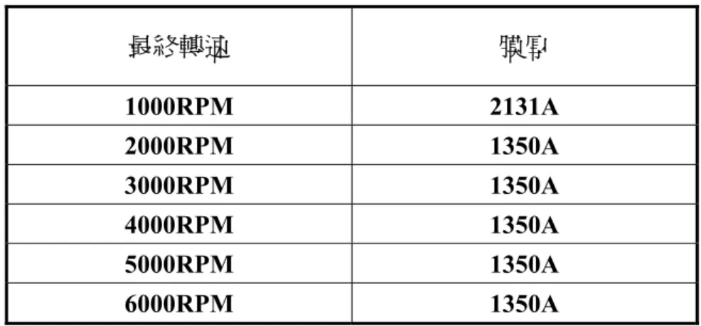
Table 2-2 shows that film thickness is independent on spin-speed when the spin-speed was
faster than 1000 rpm. We believed that the experiment result was not reliable, because P3HT was complex microstructure, in which ordered microcrystalline domains are embedded in an amorphous matrix [9]. Because the well-ordered domain is short-ranged, the data obtained by N&K analyzer is miss-matched. As a result film thickness of P3HT cannot be measured correctly by N&K analyzer.
3-3-2. Film Thickness Measurement by SEM
In the previous section we measured the film thickness of P3HT film by N&K analyzer, but
the result is not good enough. This time the SEM was performed to get an accurate result.
Experiments
The sample preparation of this experiment is the same as N&K test. Here we prepared the test samples with different P3HT film thickness made from two spin speeds, 500 and 2000 rpm.
Results and discussion
Fig.1-3 shows that 24 nm thick P3HT film can be obtained with spin speed of 2000 rpm and the uniformity is good. With a slower spin-speed the film thickness becomes un-uniformly (Fig.1-4).
3-3-3. AFM Measurement
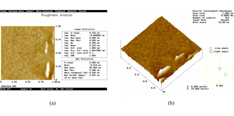
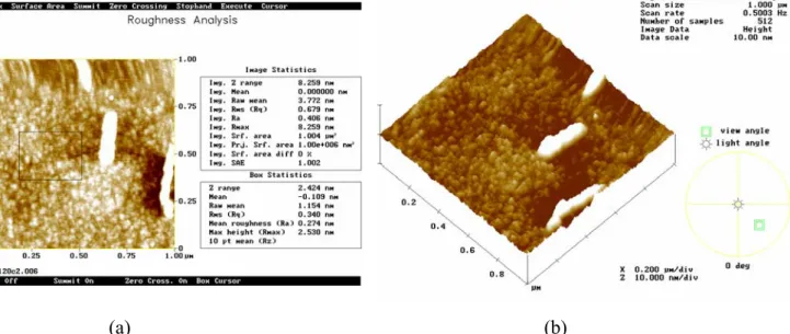
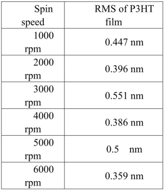
AFM was used to determine the morphology and topography of the deposited film. Fig. 1-5 shows a typical AFM micrograph showing topography of P3HT films formed by spin-coating technique. No apparent grain boundary but many clusters of undissolved P3HT powders can be observed in this AFM micrograph. Table 2-3 shows the RMS versus spin speed. It seems that RMS is not so affected by spin-speed and of the same order. Fig. 1.6, 1.7, 1.8 shows the AFM micrograph of P3HT film under different baking temperature of 170 ℃, 150 ℃ and 100 ℃ respectively. The molecular clusters are small and winded around together; no noticeable grain boundary can be found. The P3HT film we deposited by spin-coating is quite smooth without finding noticeable pinhole or defects.
By scratching the film surface and measuring the height of the step is also a possible method
to determine the correct film thickness, but the most accurate test result can only be obtained with an accurate scratching technique. The groove we made by scratching P3HT films with probe is not good enough because the width of sideline is larger than the scanning range of AFM (>5 µm).
4. Oxide Leakage Current Due to P3HT
The testing structure we used in this section was a MIS (metal-insulator-semiconductor) diode. Figure 1-9 shows the leakage current between gate and substrate of this MIS structure with 100nm SiO2 as gate dielectric. The metal area is (50 µm)^2*3.14 = 7.85*1011 cm2 . The leakage
current of bare oxide and of oxide treated with xylene was almost the same when the voltage was swept from -20V to 20V. But the leakage current of SiO2 with P3HT on its top was larger than the
formers by three orders. The large increasement in current is caused by impurity contamination of the oxide from the polymer–xylene solution [12]. As we discussed in the next chapter, the gate leakage will seriously affect the operation of OTFTs.
5 Summary
Regioregular poly-3-hexyllthiophenes (P3HTs) are important conducting polymers because
of their excellent electrical conductivity and electroluminescent and nonlinear optical properties. These polymers are soluble, thermally fusible, and environmentally stable, so they are easily processable. They are semi-crystalline in nature, and their conduction mechanism is complex. The crystalline portion can conduct current through intra-chain and inter-chain transport, whereas the amorphous portion conducts current through hopping processes. The transport of charger carriers in the P3HT film along the pi-pi stacking direction in which inter-chain transport is happened is can be formed by spin-coat technique with higher regioregular P3HT in a suitable solvent. The crystallinity of these samples may vary with the side-chain length, head-to-tail (H–T) regioregularity, molecular weight, and crystallization condition. Therefore, the conductivity and the conduction mechanism may depend on these parameters as well.
N&K method is not suitable for the measurement of P3HT film thickness, because the P3HT
film is semi-crystalline. The film thickness of P3HT film can be successfully got by using SEM. With a higher spin-speed a smooth and thin film can be formed without noticeable pinholes and defects and the thickness is about 24nm.
N
+Si
Thermal oxide
N
+Si
Doping by
PoCl3
Thermal
oxidation
P3HT
Thermal oxide
N
+Si
Deposition
of P3HT by
spin-coating
N&K test
Fig. 1-1 Chemical structure of P3HT [3] Fig.2-2 Process flow of thickness measurement by N&K analyzer
(a) (b)
Fig. 2-3 (a),(b) SEM photo : Cross-section view of test samples (upper layer is silicon wafer) made with spin speed of 2000rpm
(a) (b)
Fig. 2-4 (a),(b) SEM photo : Cross-section view of test samples (upper layer is silicon wafer) made with spin speed of 500 rpm
Fig. 1-5 Typical AFM micrograph showing topography of films formed by spin-coating technique
(a) (b)
Fig. 1-6 AFM micrograph of P3HT sample annealed at 170℃ with a (a) top-view (b) high angle view
(a) (b)
Fig. 1-7AFM micrograph of P3HT sample annealed at 150℃ with a (a) top-view (b) high angle view
(a) (b)
Fig. 1-8 AFM micrograph of P3HT sample annealed at 100℃ with a (a) top-view (b) high angle view
-20 -10 0 10 20 10-14 10-13 10-12 10-11 10-10 10-9 10-8 With P3HT treated with xylene untreated oxide oxi d e le aka ge current (A )
Voltage added to Pt contact (V)
Fig. 1-9 Gate oxide leakage current versus applied voltage
Table 1-1Field-effect mobility and on-off ratio of samples prepared from different solvents and process condition [3] 最終轉速 膜厚 1000RPM 2131A 2000RPM 1350A 3000RPM 1350A 4000RPM 1350A 5000RPM 1350A 6000RPM 1350A
Spin
speed
RMS of P3HT
film
1000
rpm
0.447 nm
2000
rpm
0.396 nm
3000
rpm
0.551 nm
4000
rpm
0.386 nm
5000
rpm
0.5 nm
6000
rpm
0.359 nm
Table 1-3 RMS measured by AFM versus spin-speed
II. Electrical Characteristic of P3HT OTFT
1. Introduction
A typical path to increase OTFTs performance could be regarded as a three-stage process: (a) A new organic semi-conductor is synthesized or a known one is used for the first time as the active layer in an OTFT. (b) The film deposition parameters for the semi-conducting organic layer are optimized to obtain the most advantageous structural and morphological characteristics for improved performance until no more improvement seems possible. (c) The source and drain contacts and the general transistor configuration are optimized. Consequently our experiment is aimed to optimize deposition parameters of spin-on P3HT and S/D contact materials of OTFTs. Additionally, the reliability test of P3HT with time and temperature is also conducted in this chapter.
2. Fabrication of OTFT
Regioregular P3HT and high purity grade solvents, xylene, were purchased from Aldrich Chemical Co. We did not perform further purification or sublimation to these chemicals. Silicon was chosen as a supporting substrate for the fabrication of OTFTs because it can be heavily doped to form a gate electrode and thermally oxidized to grow a silicon oxide insulating layer. We used two kinds of basic FET structure: top-contact and bottom-contact. As shown in Fig. 2-1 a top-contact device is with source and drain electrodes evaporated onto the organic semi-conducting layer through a metal mask. A bottom-contact device is with the organic semiconductor deposited onto the gate insulator and the pre-patterned source and drain electrodes. The polymer semiconductor layer was spin-coated on the wafer and all chemicals were filtered through a 0.20um pore-size PTFE filter before deposition. Typical film thickness after spin-coating are 10~100nm. All samples were handled in the air.
2-1. Modification of oxide surface
Oxide surfaces were treated with hexamethyldisilazane (HMDS) to improve the adhesion between polymer chain and oxide surfaces. Modification of the substrate surface prior to deposition of regioregular P3HT has also been found to influence film morphology. For example, treatment of SiO2 with hexamethyldisilazane (HMDS) or an alkyltrichlorosilane replaces the hydroxyl groups at the SiO2 surface with methyl or alkyl groups. The apolar nature of these groups apparently attracts the hexyl side chains of P3HT, favoring lamellae with an edge-on orientation (Fig. 2-2) [9]. According to [9], the mobility of OTFTs with an edge-on orientation P3HT film is high than the one with a face-on orientation.
2-2. Fabrication of Top-Contact (TC) structure device
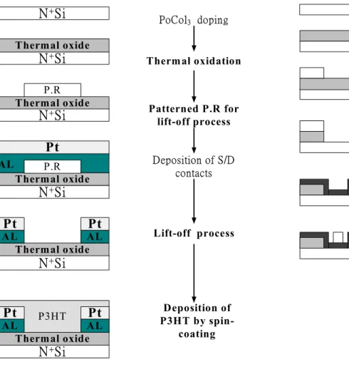
To construct the top-contact type device, we first fabricated the OTFTs by spin coating a film of P3HT onto a highly doped n+ Si wafer with a 1000 Å SiO2 gate oxide (capacitance Ci = 34 nF*cm–2). Platinum, aluminum and nickel source-drain contacts were subsequently deposited onto the P3HT through a shadow mask. Typical channel width, W, is in a range of 100~5000um and typical channel length, L, is in a range of 30~200um.The process flow is shown in Fig. 2-3.
2-3. Fabrication of Bottom-Contact (BC) structure device
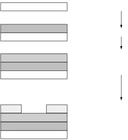
Heavily doped n+ silicon wafer (resistivity 7 ohm-cm) was used as a common gate contact. An insulating layer of silicon dioxide is thermally grown (1000 Å). Aluminum (1000 Å) which acts as an adhesion layer, followed by Pt (500 Å), is evaporated and lifted off to form source and drain contacts. An interdigitated geometry for the source-drain contacts is chosen to minimize the contact area and the associated gate to source-drain leakage current. Fig. 2-4 shows the cross-section view of a device with finger-shaped S/D contacts. Typical channel width, W, are in a range of 100~10000 um and typical channel length, L, is in a range of 10~50um. Finally, the devices are completed by depositing of a P3HT semi-conducting layer. The process flow is shown in Fig. 2-5.
2-4. Fabrication of BC structure OTFT with Pre-patterned Gate Oxide
In order to lower the gate leakage current and but not to increase the working bias of gate side, we fabricated the BC structure OTFT with a gate trench. The only difference in process steps is the etch step for gate oxide trench. Process flow is shown in Fig. 2-6.
2-5. Measurement
Current-voltage characteristics of OTFT were measured in the air with a semiconductor parameter analyzer HP4156. All measurements were carried out in an electrically shielded box. The drain-source current, Ids, was measured as a function of the drain-source voltage, Vds, to observe FET-like characteristics, while plots of Ids Versus gate-source voltage, Vgs, were constructed to determine the gate bias modulation of the FET conductive channel.
Three parameters were extracted from the experimental I-V curve and are: (1) the bulk conductivity of P3HT thin film (σ); (2) the transistor threshold voltage (Vth); (3) the field effect mobility (µ); (4) the current modulation (the ratio of the current in the accumulation mode over
the current in the depletion mode, also referred to as ON-OFF current ratio). The detail extraction method will be discussed in the following section.
3. Operation of OTFT
The operation of OTFT is refer to [11] and described below. Organic TFTs are primarily operated as accumulation-mode enhancement type transistor, which are opposed to the usual inversion mode operation of silicon MOSFETs. Ideally the source and drain contacts should behave as ohmic contacts for the majority carrier in the organic semiconductor.
In Fig. 2-7 (a), a schematic diagram is shown, in which zero bias was applied to all three contacts of an OTFT. If a small drain bias, Vd, is applied then the source-drain current, Ids, will be small and ohmic.
If a negative bias, Vg, is applied to the gate electrode (Fig. 2-7 (b)), the voltage is dropped over the insulator and over the semiconductor near insulator/semiconductor interface, giving rise to band bending in the semiconductor, the accumulation region. The additional positive charge accumulated in this region is supplied by the ohmic source and drain contacts. The semiconductor now contains positive charges both from doping and from the ‘field effect’ which created the accumulation layer. When a small bias is applied on the drain contact, a current larger than the ohmic current will be measured.
If a positive gate bias is applied, then the opposite band bending occurs in the semiconductor at the insulator interface, leading to depletion of charge (Fig. 2-7(c)). Inversion mode cannot be observed in the organic TFTs since the metal contacts are ohmic contacts for electron injection into the organic semiconductors.
As the drain bias becomes increasingly negative, the accumulation charge density will decrease from source to drain contact (Fig. 2-7 (d)). If the drain becomes more negative than the gate then a depletion zone will begin to appear and grow from the drain contact (Fig. 2-7 (e)).
4. Electrical characteristics of P3HT OTFT
A typical plot of drain current Id versus drain voltage Vd at various gate voltages Vg is shown in Fig. 2-8 which illustrates the operation of top-contact OTFT using a semi-crystalline, spin-coated P3HT film as a semi-conducting layer. The transistor was measured in atmosphere. The devices channel length/width was 30µm/ 5000µm. The film thickness measured by SEM was 24 nm. The result shows the FET-like Id-Vd curve of P3HT OTFT. Drain current increased linearly when drain bias was small and then saturated when drain bias was high enough to pinch off the channel.
Fig. 2-9 (a) shows a gate sweep at a drain bias of -5V. The gate bias was swept from +40V to -50V. Like p-type OTFTs, for negative gate bias the current increases and for positive gate bias the current decreases. Fig. 2-9 (b) shows that mobility increases with gate bias, which is consistent with a multiple trapping and release model [13]. The observed decrease in mobility at larger gate bias may be due to increased interface scattering. The best linear mobility of P3HT OTFT we made is about 10-2 cm2/Vs and the on-off ratio is about 103.
5. The Gate Leakage Current Effect on OTFT
is coated on it. Fig. 2-10 is a plot of drain current and gate leakage current versus gate voltage. When the OTFT was turned on, the ‘on-current’ was larger than the gate leakage current by one order. The gate leakage current was comparable to the drain current when the device is nearly turned off, finally the gate leakage current dominated the drain current. In that situation, we cannot measure the ideal I-V characteristics because the gate leakage current is quite large. As a result, the ON-OFF current ratio would be affected by gate leakage current.
As shown in Fig. 2-11, the source current at zero drain bias would be affected by gate leakage current strongly. The gate leakage current is of the same order in the two devices. When the leakage current is comparable to the source current of the OTFT with small W/L ratio, the result would be incorrect.
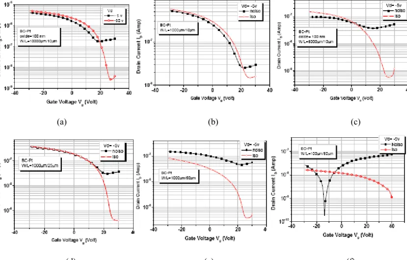
The P3HT film collected the gate leakage current causing to the overestimation of drain current. In order to reduce this problem, we scraped the P3HT film outside the active region to isolate the devices. Fig. 2-12 shows that after the scraping step the current can be reduced at least two orders. As a result, it is necessary to pattern the P3HT film to reduce the gate leakage problem.
Knowing that the gate leakage is a serious problem, we fabricated the BC OTFT which has less overlap area of P3HT and oxide. Fig.2-13 shows that the gate leakage current of OTFT with patterned oxide and P3HT film is the smallest due to the thick oxide thickness under the S/D region. BC-OTFT works well to reduce the gate leakage current by reducing the gate leakage current outside the channel from common gate oxide below S/D contacts and outside the active region. The leakage current effect on the drain current would affect the test result of conductivity of OTFT by overestimating the drain current at low drain bias.
6. Electrical characteristics of OTFT with different W/L ratio 6-1. Mobility of OTFT with different W/L ratio
The linear regime field effect mobility can be obtained by the calculation described below. At low VD, ID increases linearly with VD (linear regime) and is approximately determined from the following equation:
(3-1)
where L is the channel length, W is the channel width, Ci is the capacitance per unit area of the insulating layer, VT is the threshold voltage, and µ is the field effect mobility, which can be calculated in the linear regime from the transconductance,
(3-2)
by plotting ID versus VG at a constant low VD, with -VD << -(VG - VT), and equating the value of the slope of this plot to gm.
Fig. 2-14 is the plot of mobility versus channel length. All devices are TC structure with Ni S/D contacts and with the same channel width (5000µm). As expected, mobility generally increases with increasing channel length, as the relative influence of the contacts is reduced.
6-2. Threshold Voltage of OTFT with different W/L ratio
with Ni S/D contacts and with the same channel width (5000µm). The threshold voltage generally decreases with increasing channel length but the difference is small. The results show that W/L ratio is not an issue of threshold voltage.
6-3. On-Off Ratio of OTFT with Different W/L Ratio
We used the ratio of the current in the accumulation mode over the current in the depletion mode as the calculation method. Figure 2-16 (a) shows that the on-off ratio increased largely with increasing W/L ratio. The results shows that device with larger W/L ratio has a better channel modulation ability. But the extraction method of on-off ratio we used in this section would affect seriously by gate leakage current. Now, we used another definition about on-off ratio. We defined the on/off ratio at a given negative drain bias as the ratio of the current in a transistor in its ‘on-state’, Vg = Vd < 0V, to the current in its ‘off-state’, Vg = 0V, Vd < 0V. By using this definition, we get another test result as showed in fig. 2-16 (b). The test result shows that that device with larger W/L ratio has a better channel modulation ability but the value is very small due the effect of doping by oxygen which caused the shift of threshold voltage.
In that situation, the device is already turned on when Vg = 0V.
7. Electrical characteristics of OTFT under Different Operation Temperature
In order to investigate the effect of temperature on mobility, conductivity, and on-off ratio, measurements under different temperature were performed.
7-1. Mobility of OTFT under different operation temperature
Fig.2-17 shows that the field effect mobility increased with increasing temperature. It is generally agreed that charge transport in organic semiconductors occurs via hopping of self-trapped polarons [14]. Evidence for hopping transport mostly relies on the fact that the field-effect mobility of organic semiconductors is thermally activated [14].
The weak intermolecular interaction forces in organic semi-conductors (van der Waals interaction), may be responsible for the low mobility of OTFT. In contrast, in inorganic semiconductors such as Si, Ge, and GaAs, the atoms are held together with very strong covalent bonds [1]. Band transport is not applicable to disordered organic semiconductors, where carrier transport takes place by hopping between localized states and carriers are scattered at every step [1]. Hopping is assisted by phonons and the mobility increases with temperature, although typically it remains very low overall (l << cm2V-1 s-1). The boundary between band transport and hopping is defined by materials having RT mobilities of the order of 1 cm2V-1 s-1.
7-2. Conductivity of OTFT under different operation temperature
Extraction method
The extraction method is refer to [15] and described below.
The total current of a polymer-FET was separated into two components: channel current (Ich) and bulk current (Ibk). With use of established metal-oxide-field effect transistor (MOSFET) current-voltage relationships, the channel current can be formulated as
Ich = Ì*Cox W /L (Vgs - Vt)Vds – 1/2Vds 2
threshold voltage; Ì is the carrier mobility; and Cox is the capacitance of the oxide layer. The bulk current can be represented as
Ibk= µ*W/L*l*Vds (3-4) where l is the polymer layer thickness.
In our analysis of Ids - Vds responses, three assumptions are made:(1) The current at zero gate bias is considered to be the Ohmic current that flows through polymer substrate. The channel current below the threshold voltage is negligible compared with the bulk region current. (2) Bulk current at positive gate biases is equal to that at zero gate bias. The accumulation layer thickness is comparatively much smaller than the polymer bulk thickness, therefore the bulk region thickness does not show a considerable change upon formation of an accumulation layer. (3) Mobility is considered only to be a weak function of gate bias, especially in the low-voltage range (0 to -30 V). Based on these above assumptions and equations, the bulk conductivity can be determined from IDS - VDS at zero bias.
Results
Fig. 2-18 shows the conductivity of P3HT increased with increasing operation temperature. It means that the conductivity of P3HT is thermal activated.
8. Mobility Comparison between TC and BC OTFT
Top contact device yield mobilities that are typically larger by a factor compared to bottom contact devices. But in our experiment results, the mobility of BC OTFT with Pt S/D contacts (about 10-3 cm2V-1 s-1) is higher than TC OTFT with the same Pt S/D contacts (about 10-4 cm2V-1 s-1). We think that the contact resistance effect lowers the mobility of TC OTFT. Because the carriers in the TC OTFT must go through the P3HT film vertically below the region of S/D contacts. The deposition onto a flat surface was also found to be advantageous relative to coating the polymer onto a substrate with prefabricated source-drain contacts [8]. The more ordered morphology of TC OTFT made better mobility. Grain boundaries between the small crystalline domains with more disordered chain conformation, residual doping, and other structural or chemical defects give rise to localized trap states [4].
9. Time Evolution of Electrical characteristics with Time
All organic devices show bad stability with time compared to inorganic devices. The OTFT we fabricated is without a passivation layer. In that situation we expect that the OTFT will suffer from doping by oxygen molecular in air. We store the devices in boxes and measure them after several days to see the variation of electrical characteristics with time.
9-1. Conductivity
Figure 2-19 (a) shows the conductivity versus time. The conductivity of P3HT increases on exposure to air, oxygen in particular [15].As expected the conductivity generally increases with time, especially the first two days. Then the conductivity saturated beyond two days. But for the device with higher W/L ratio, the conductivity decreases instead of increasing beyond two days due to the degradation of OTFT which lowers the on-current at Vg = 0 V (fig. 2-19 (b)).
9-2. Mobility
Fig. 2-20 shows that mobility generally decreases with increasing storage time. The mobility increase with increasing doping concentration, this effect dominates the conductivity results for first few days. But eventually the mobility decreases due to degradation of device.
9-3 Threshold voltage
Fig. 2-21 (a) and (b) shows the plot conductivity versus time with the same channel width 1000µm, and with the same channel length 10µm respectively. As mention before conductivity is not affect by W/L ratio. Threshold voltage generally increased with time especially in the first few days and saturated slowly to the solubility upper-limit of doping concentration. Conductivity that arises from dopants is depletable in our case, resulting in a threshold or a turn-on voltage opposite in sign from the accumulation regime.
9-4. The relationship between conductivity and mobility
As shown in fig. 2-22(a), the relationship between the conductivity and mobility increase is similar for a wide variety of compounds with intrinsic mobility below 0.001 cm2/Vs, as suggested by the plot in fig. 2-22 (b)[12]. The line has been plotted which has the simple power law from given by
μ= σδ. (3-5)
The value of δ obtained in our experiment, δ = 1.1, is larger than the value of world wide conjugated materials, δ = 0.7. This may result from the degradation of device which lowers the mobility.
For heavily doped systems charge transport is dominated by variable-range hopping at the Fermi level. The mobility will increase with conductivity [12].
9-5. Discussion
The field-effect mobility can be increased by two to three orders of magnitude by addition of more charge carriers, by doping. The plausible explanation for the increase is either filling of the traps and/or defects in the polymer structure by additional doping and/or, shortening of mean free path for the charge carriers because of increased number of carriers [16]. However, additional doping reduces the ratio since the polymer now has a higher electrical conductivity, and hence a higher “off-current”. Although in our experiment the On-off ratio is not so accurate to see the result mention by other researchers due to the gate leakage effect.
Due to the underlying hopping transport of charge carriers the field-effect mobilities could be increased by doping but only at the expense of increased bulk conductivity. This then yields transistors which have insufficient current modulation for application.
10. Contact resistance of OTFT
Introduction
Unlike in field effect transistors based on inorganic materials, the source and drain contacts in organic TFTs are not easily optimized by conventional processes, such as semiconductor doping or metal alloying. Consequently, organic TFT performance typically suffers from large contact resistance. For example, this resistance may mask a mobility that increases with gate voltage, as
the resistance becomes a dominant circuit element [17].
Both work function mismatches between metal and semiconductor and chemical reactivity of metals with the semiconductors may contribute to this resistance [17].
Experiments
In our experiment, we used three different Source/Drain contacts: aluminum, Platinum, and Ni. By the contact resistance test, we expect to compare the different electrical characteristics of the three kinds of contact metals with different work function, then to make the best choice of S/D contact metal for OTFT.
The parameter extraction method of contact resistance is refer to [18] and described below. Assuming that the resistance at the source and drain contacts is independent of the potential drop across the contacts, the contact resistance can be estimated by plotting the inverse of drain current versus channel length, extrapolating to a channel length of zero (where the channel resistance disappears), and multiplying by the drain–source voltage. The channel resistance per channel length is given by the slope of the inverse of drain current versus channel length curve, multiplied by the drain–source voltage.
Results and Discussion
Figure 2-23 and 2-24 show the test result of TC OTFT with Pt and Ni S/D contacts respectively. Contact resistance of TC structure with Pt contacts is larger than the one with Ni contacts. By comparing the difference of work function between S/D contacts and P3HT, we found that the larger the work function difference the larger the contact resistance was. Work function differences made the different contact resistance. As a result, the work function of S/D contacts must match the one of P3HT to keep the contact resistance low for TC structure.
Fig.2-25 shows the channel resistance per 1µm channel length for P3HT OTFTs with a channel width of 5000µm. As expected, contact resistance decreases with increasing gate bias, due to the increase in carrier density in the channel. The channel resistance with drain bias = -40 V increased sharply at Vg < 0V due to the channel pinch-off at drain site. Finally when the device was turned off the channel resistances were almost the same.
We do not show the contact resistance result of OTFT with Al S/D contacts, because the plot of Id-Vd curve is not FET-like (fig. 2-26), thus we can not get a correct extraction result. Therefore, the schottky-type contact is not suitable for OTFTs.
11. Mobility (channel resistance concerned)
Introduction
The mobility determined by using conventional MOS parameter extraction methods does not include the effect of the channel resistance. Furthermore, any variation of the mobility with voltage dependent variables, such as electric field or free carrier concentration, cannot be detected.
Here we used the method invented by Gilles Horowitz, et al [14] as described below. The original model is improved by accounting for the contact resistance at source and drain. For this, we add the voltage drop through a series resistance, Rs:
First, we estimate the drain conductance gd and transconductance gm at a low drain voltage, which are defined by Eqs. 3-7 and 3-8, respectively,
(3-7) (3-8)
To eliminate the series resistance, we divide Eq.3-7 by the square root of Eq.3-8 and after some manipulations, we finally obtain Eq.3-9:
(3-9)
We measure the transfer (Id–Vg) characteristic of the transistors at a low drain voltage (Vd= -5V), and perform a numerical derivation of Eq.3-9.
Results and Discussion
Fig. 2-27 shows that the corrected mobility was smaller than the uncorrected one. The corrected mobility is gate-voltage dependent and increased generally linearly with gate bias and saturated at higher gate voltage. A possible explanation for the gate-voltage dependent of the mobility is that charge carrier concentration accumulated near the in the channel increases linearly with increasing gate voltage, and the hypothesis is still investigating by Gilles Horowitz, et al [14]. The origin model without considering the effect of contact serious resistance leads to an overestimation of the field effect mobility.
12. Organic Film Thickness Dependence of Mobility
As shown in fig. 2-28, the mobility with thick P3HT film is larger than the thin one by one order. This may be due to the better molecular morphology formed in the thick P3HT film. The presence of a highly ordered bulk in thicker films may also exert an ordering effect onto the interfacial layer [19].
13 Summary
The Id-Vd curve of P3HT OTFT we made is FET-like. Drain current increased linearly when drain bias was small and then saturated when drain bias was high enough to pinch off the channel. As for Id-Vg curve, for negative gate bias the current increases and for positive gate bias the current decreases. The result of Id-Vg curve shows p-type behavior. The linear mobility increases with gate bias, which is consistent with a multiple trapping and release model.
The off-current of P3HT OTFT is affected by gate leakage current. Therefore we cannot get an accurate on-off ratio. The bottom-contact structure OTFT works well to reduce the gate leakage current. After all, we had better to pattern the P3HT active layer to get an accurate test result without the influence of gate leakage effect.
The W/L ratio influences the mobility of OTFTs. With the same channel width, the motility increased with increasing channel length due to the reduction of contact resistance effect.
The mobility increased with increasing operation temperature. The thermal activated mobility is an evidence of hopping transport mechanism for organic materials with mobility less than 1 cm2/Vs.
In the stability test, interaction between molecular oxygen and P3HT caused an increase to conductivity of P3HT and threshold voltage of OTFT. In the same time the performance of OTFT would grow weak with increasing time.
difference of work function between S/D contacts and P3HT is needed for a better device performance. With a better S/D contacts the contact resistance is small, thus a better performance is expected. In contrast, with a schottky-type S/D contacts the electrical characteristics of OTFT is not FET-like, because the charge carriers cannot inject form S/D through a high barrier formed on interface between S/D contacts and P3HT.
The relationship between conductivity and mobility we obtained is followed by a power law for conjugated materials. This is also an evidence of hopping transport mechanism.
The mobility with a thick P3HT film is large, and this may be due to the result of better morphology formed inside the P3HT bulk.
Fig. 2-1 A top-contact device is with source and drain electrodes evaporated onto the organic semi-conducting layer through a mask. A bottom-contact device is with the organic semiconductor deposited onto the gate insulator and the prefabricated source and drain electrodes.
Egde-on orientation Face-on orientation
Fig. 2-2 Two different orientations of ordered P3HT domains with respect to the FET substrate [9]
Fig. 2-3 Process flow of top-contact OTFT
P3HT
Thermal oxide
AL
Pt
AL
Pt
N
+
Si
(a) (b)N+Si PoCol3 doping Thermal oxidation Patterned P.R for lift-off process Deposition of S/D contacts Lift-off process Thermal oxide N+Si Thermal oxide N+Si P.R AL Thermal oxide N+Si P.R Pt Thermal oxide ALPt ALPt N+Si P3HT Thermal oxide ALPt ALPt N+Si Deposition of P3HT by spin-coating
Fig. 2-5 Process flow of bottom-contact OTFT Fig. 2-6-1 Process flow of bottom-contact OTFT with patterned gate oxide
Fig. 2-7 Operation of OTFT [12] (a) No-bias (b) Accumulation mode (c) Depletion mode (d) Non-uniform charge density (e) Pinch-off of channel (f) and (g) Growth of the depletion zone.
-4 -2 0 -5.0x10⁻⁷ 0.0 TC-Ni W/L=5000µm/30µm Drai n current( A ) Drain voltage (V) V g = (v) 22.5 15 7.5 0 -7.5 -15 -22.5 -30 -40 -30 -20 -10 0 10 -3.0x10⁻⁶ -2.5x10⁻⁶ -2.0x10⁻⁶ -1.5x10⁻⁶ -1.0x10⁻⁶ -5.0x10⁻⁷ 0.0 5.0x10⁻⁷ TC-Ni W/L=5000µm/30µm Dr ain curr ent( A) Drain voltage (V) Vg = (v) 22.5 15 7.5 0 -7.5 -15 -22.5 -30 (a) (b)
Fig. 2-8 Typical FET-like Id-Vd curve: (a) Linear region when Vd is small (b) Saturated region when Vd is large
-20 0.0 2.0x10⁻³ 4.0x10⁻³ 6.0x10⁻³ 8.0x10⁻³ 1.0x10⁻² 1.2x10⁻² 0 20 TC-Ni oxide=100nm W/L=5000µm/30µm Mo bi li ty ( c m 2/V s)
Gate Voltage Vg (Volt)
Vd= -5v -60 -40 -20 0 20 40 10-9 10-8 10-7 10-6 10-5 10-4 TC-Nioxide=100nm W/L=5000µm/30µm Drai n Cu rr e n t ID (Amp) Gate Voltage V g (Volt) Vd= -5v
(b)
Fig. 2-9 (a) Typical Id-Vg curve of P3HT OTFT: Ig increases with increasing negative gate bias (b) Mobility of P3HT OTFT increases with increasing negative gate bias then decreased due to surface scattering effect.
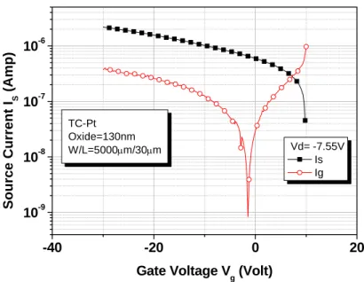
-40 -20 0 20 10-9 10-8 10-7 10-6 TC-Pt Oxide=130nm W/L=5000µm/30µm Source Current I S (A m p )
Gate Voltage Vg (Volt)
Vd= -7.55V Is Ig
Fig. 2-10 Source and gate leakage current versus gate bias
-20 -15 0.0 5.0x10⁻⁸ 1.0x10⁻⁷ 1.5x10⁻⁷ 2.0x10⁻⁷ 2.5x10⁻⁷ 3.0x10⁻⁷ -10 -5 0 TC-Pt Oxide=50nm W/L=100µm/30µm Drain bias (V) Source c u rrent ( A ) V g= 10 2 -6 -14 -22 -30 -20 -15 -10 -5 0 0.0 5.0x10⁻⁷ 1.0x10⁻⁶ 1.5x10⁻⁶ 2.0x10⁻⁶ 2.5x10⁻⁶ 3.0x10⁻⁶ 3.5x10⁻⁶ TC-Pt Oxide=50nm W/L=5000µm/30µm Sour ce cur rent (A ) Drain bias(V) Vg= (V) 10 2 -6 -14 -22 -30 (a) (b)
Fig. 2-11 Influence of gate leakage current on Id-Vd: (a) TC OTFT with W/L = 5000µm/30µm (b) TC OTFT with W/L = 100µm/30µm
(a) (b) (c)
(d) (e) (f)
Fig. 2-12 Id-Vg curve of patterned and non-patterned P3HT BC OTFT with (a) W/L = 10000µm/10µm (b) W/L = 5000µm/10µm (c) W/L = 1000µm/10µm (d) W/L = 1000µm/25µm (e) W/L = 10000µm/50µm (f) W/L = 100µm/50µm
(a) (b)
(c)
Fig 2-13 Id-Vd curve of BC OTFT with (a) non-patterned oxide (b) patterned oxide (c) patterned oxide and P3HT film
0 50 100 150 200 1.1x10⁻² 1.2x10⁻² 1.3x10⁻² 1.4x10⁻² 1.5x10⁻² 1.6x10⁻² 1.7x10⁻² 1.8x10⁻² mobil it y (cm 2 /V* s ) channel length(µm) linear mobility Vd= -5 V TC-Ni W=5000µm
Fig.2-15 Threshold voltage of TC OTFT with Ni S/D contacts versus channel length
Fig. 2-16 On-off ratio versus time measured by definition: (a) I on (Vg = Vd < 0)/ I off
Fig.2-17 Mobility of BC OTFT w
(Vg=0,Vd<0) (b) Ion(accumulation mode)/ I off (depletion mode)
20 30 40 50 60 70 80 90 100 110 1.0x10⁻³ 2.0x10⁻³ 3.0x10⁻³ 4.0x10⁻³ 5.0x10⁻³ Vd= -5v W/L= (µm/µm) 100/50 300/50 500/50 mob ilit y (c m 2 /V *s ) Temp (C) BC-Pt
ith Pt S/D contacts measured under different operation temperature
(a) (b)
(c)
Fig. 2-18 Conductivity of P3HT film versus op on temperature measured from BC OTFTs (a)
)
Fig. 2-19 Conductivi µm /10µm
erati
with channel length of 50µm (b) with channel width of 1000µm (c) with channel length of 10µm
(a (b) ty and mobility of P3HT versus time with device (a) W/L= 1000 (b) W/L= 5000µm /10µm
Fig. 2-20 Mobility of BC OTFT with Pt S/D contacts versus time
(a)
Fig. 3-21 Threshold voltage of BC OTFT versus time with (a) the same channel width of 1000µm (b) the same channel len
(b)
gth of 10µm
(a) (b)
Fig. 3-22 Field-effect mobility plotted against the bulk conductivity from (a) experiment result of P3HT (b) some conducting polymers (from [12])
(a) (b)
Fig. 3-23 Contact resistance of TC OTFT with Pt S/D contacts measured when device is operated in (a) linear region (b) saturated region
(a) (b)
Fig. 3-24 Contact resistance of TC OTFT with Ni S/D contacts measured when device is operated in (a) linear region (b) saturated region
(a) (b) Fig. 3-26 (a) Id-Vd curve (b) Id-Vg curve of TC OTFT with Al S/D contacts
Fig. 3-27 Original and corrected mobility of TC OTFT with Ni S/D contacts versus gate bias
Fig. 3-28 The mobility of TC OTFT with Ni S/D contacts and different P3HT film thickness versus channel length
REFERENCE
imitrakopoulos, Parick R. Malenfant, “Organic thin film transistors for large
area electronics” Adv. Mater. 2002, 14, No2, January 16
1988
pol
[1] Christos D. D
[2] A. Assadi, C. Svensson, M. Willander, O. Inganas, “Field-effect mobility of
poly(3-hexylthiophene)” Appl. Phys. Lett. 53(3), 18 July
[3] Bao, Z.; Lovinger, A. J, “Soluble Regioregular Polythiophene Derivatives as Semiconducting
Materials for Field-Effect Transistors” Chem. Mate.(Article); 1999
[4] Sirringhaus, Henning; Tessler, Nir; et al. ; ”Integrated optoelectronic devices based on conjugated
ymers”, Science, 06/12/98, Vol. 280 Issue 5370, p1741
[5] Sirringhaus, H.; Brown, P.J.; Friend, R.H.; Nielsen, M.M.; Bechgaard, K.; Langeveld-Voss,
B.M.W.; et. al. ”Microstructure–mobility correlation in self-organised, conjugated
polymer field-effect transistors” Synthetic Metals Volume: 111-112, June 1, 2000, pp.
129-132
Cheng Yang, Francesco P. Orfino, and Steven Holdcroft, “A Phenomenological Model for
Predictin
[6]
g Thermochromism of Regioregular and Nonregioregular
[7]
poly(3-alkylthiophenes)” Macromolecules, Vol. 29, No. 20, 1996
Amundson, Karl R.; Sapjeta, B. Joyce; Lovinger, Andrew J.; Bao, Zhenan “An in-plane
anisotropic organic semiconductor based upon poly(3-hexyl thiophene)” Volume: 414,
[8]
e) for thin film field-effect transistor applications with
[9]
. Herwig & D. M. de
[10
Substituted α,ω-Dialkyl Thiophene
[11] ing conjugated [12] A s hys., Vol. 85, [15] Issue: 1, July 1, 2002, pp. 143-149
Zhenan Bao,a) Ananth Dodabalapur, and Andrew J. Lovinger ; “Soluble and processable
regioregular poly(3-hexylthiophen
high mobility” Appl. Phys. Lett., Vol. 69, No. 26, 23 December 1996
H. Sirringhaus, P. J. Brown, R. H. Friend, M. M. Nielsen, K. Bechgaard, B. M. W. Langeveld-Voss, A. J. H. Spiering, R. A. J. Janssen, E. W. Meijer, P
Leeuw; “Two-dimensional charge transport in self-organized, high-mobility conjugated
polymers” NATURE |VOL 401 | 14 OCTOBER 1999
] Howard E. Katz,* Joyce G. Laquindanum, and Andrew J. Lovinger ; “Synthesis, Solubility,
and Field-Effect Mobility of Elongated and
Oxa-Oligomers. Extension of “Polar Intermediate” Synthetic Strategy and Solution Deposition on Transistor Substrates” ; Chem. Mater. 1998, 10, 633-638
Giles Lloyd , Munira Raja , Ian Sellers , Naser Sedghi , Raffaella Di Lucrezia , Simon Higgins , Bill Eccleston ; “The properties of MOS structures us
polymers as the semiconductor” ; Microelectronic Engineering 59 (2001) 323–328
.R. Brown, C.P. Tarrett, D.M. de Leeuw, M. Matters; “Field-effect transistor made from
olution-processed organic semiconductors” ; Synthetic Metals 88 (1997) 37-55
[13] P. V. Necliudov and M. S. Shur; “Modeling of organic thin film transistors of different
designs” ; JOURNAL OF APPLIED PHYSICS VOLUME 88, NUMBER 11
[14]Gilles Horowitz,a) Riadh Hajlaoui, Denis Fichou, and Ahmed El Kassmi; “Gate voltage
dependent mobility of oligothiophene field-effect transistors” ; J. Appl. P
No. 6, 15 March 1999
“Interaction of Oxygen with Conjugated Polymers: Charge Transfer Complex
[16]
998)
[17] H
J. Phys. Chem. B 2000, 104, 671-678
as N.Jackson; “Contact resistance in organic
[19]
thiophene) Field-Effect
計畫
1. S. C. Wang, J. C. Lou, B. L. Liou, R. X. Lin, and C. F. Yeh, “Process Improvement and Reliability Characteristics of Pin-on Poly-3-hexylthiophene Thin-Film Transistor, "
Formation with Poly(3-alkylthiophenes) “ ; J. Am. Chem. Soc. 1997, 119, 4518-452
Y. Harima, T. Eguchi, K. Yamashita; “Enhancement of carrier mobility in
poly(3-menthythiophene) by an electrochemical doping” ; Synthetic Metals 95 (1
69-74
. E. Katz* and Z. Bao; “The Physical Chemistry of Organic Field-Effect Transistors” ;
[18] Hagen Klauk, Gunter Schmid, Wolfgang Radlik, Werner Weber, Lisong Zhou, Chris D.Sheraw, Jonathan A.Nichols, Thom
thin .lm transistors” ; Solid-State Electronics 47 (2003) 297–301
Henrik G. O. Sandberg, Gitti L. Frey, Maxim N. Shkunov, Henning Sirringhaus, and Richard H. Friend; “Ultrathin Regioregular Poly(3-hexyl
Transistors” ; Langmuir 2002, 18, 10176-10182
成果自評
![Fig. 2-2 Two different orientations of ordered P3HT domains with respect to the FET substrate [9]](https://thumb-ap.123doks.com/thumbv2/9libinfo/8516708.186229/22.892.190.726.724.951/fig-different-orientations-ordered-domains-respect-fet-substrate.webp)
![Fig. 2-7 Operation of OTFT [12] (a) No-bias (b) Accumulation mode (c) Depletion mode (d) Non-uniform charge density (e) Pinch-off of channel (f) and (g) Growth of the depletion zone](https://thumb-ap.123doks.com/thumbv2/9libinfo/8516708.186229/25.892.271.620.49.466/operation-accumulation-depletion-uniform-density-channel-growth-depletion.webp)