行政院國家科學委員會專題研究計畫 成果報告
氮化鎵介觀尺度下量子局限結構之光子幅射可控性研究
(3/3)
研究成果報告(完整版)
計 畫 類 別 : 整合型 計 畫 編 號 : NSC 94-2120-M-009-007- 執 行 期 間 : 94 年 08 月 01 日至 96 年 07 月 31 日 執 行 單 位 : 國立交通大學光電工程學系(所) 計 畫 主 持 人 : 王興宗 共 同 主 持 人 : 孟心飛、彭隆瀚、林恭如、郭浩中 計畫參與人員: 學士級-專任助理:劉淑致、邱麗君 博士班研究生-兼任助理:姚忻宏、薛道鴻、張亞銜、賴芳 儀、巫漢敏、張詒安、高志強、林俊榮、朱榮堂、王德忠、 柯宗憲、羅明華、陳士偉、邱清華 碩士班研究生-兼任助理:張峻瑋、歐陽妙佳、謝永龍、陳威 佑、余國正、王薏婷、梁文燈、羅傳煜、彭裕鈞、蔡敏瑛、 朱瑞溢、高宗鼎、葉剛帆、林皇伸、游敏、蘇柏傑、林立 凡、蔡孟儒、劉瑞農、李卓奕、朱家璞、高潤琪、劉子維 博士後研究:黃根生、陳厚光 報 告 附 件 : 出席國際會議研究心得報告及發表論文 處 理 方 式 : 本計畫可公開查詢中 華 民 國 96 年 12 月 07 日
行政院國家科學委員會補助專題研究計畫
■ 成 果 報 告
□期中進度報告
Research on Mesoscopic GaN Quantum Confined Structures
for Control of Photon Emission
氮化鎵介觀尺度下量子局限結構之光子幅射可控性研究
計畫類別:
■
個別型計畫 □ 整合型計畫
計畫編號:NSC 92-2120-M-009-006
執行期間:92 年 08 月 01 日至 95 年 07 月 31 日
計畫主持人:S. C. Wang(王興宗)
共同主持人:
H. C. Kuo (郭浩中)、H. F. Meng(孟心飛)、L.-H. Peng(彭
隆瀚)
、
Gong-Ru Lin(林恭如)
計畫參與人員:
張連璧(博士後)、黃根生(博士後)、劉淑致(研究助理)、邱麗君 (研究助理),博士生︰姚忻宏、薛道鴻、張亞銜、賴芳儀、巫漢敏、張怡安、高志強、林 俊榮、朱榮堂、王德忠、柯宗憲、羅明華、陳士偉、邱清華;碩士生︰張峻瑋、歐陽妙佳、 謝永龍、陳威佑、余國正、王薏婷、梁文燈、羅傳煜、彭裕鈞、蔡敏瑛、朱瑞溢、高宗鼎、 葉剛帆、林皇伸、游敏、蘇柏傑、林立凡、蔡孟儒、劉瑞農、李卓奕、朱家璞、高潤琪、 劉子維。成果報告類型(依經費核定清單規定繳交):□精簡報告 ■完整報告
本成果報告包括以下應繳交之附件:
□赴國外出差或研習心得報告一份
□赴大陸地區出差或研習心得報告一份
■出席國際學術會議心得報告及發表之論文各一份
□國際合作研究計畫國外研究報告書一份
處理方式:除產學合作研究計畫、提升產業技術及人才培育研究計畫、
列管計畫及下列情形者外,得立即公開查詢
□涉及專利或其他智慧財產權,□一年□二年後可公開查詢
執行單位:
Research on Mesoscopic GaN Quantum Confined Structures for
Control of Photon Emission
氮化鎵介觀尺度下量子局限結構之光子幅射可控性研究
總執行期限:2003/08/01 ~2006/07/31
PI:S. C. Wang(王興宗), National Chiao-Tung University, E-mail: [email protected] Co-PI:H. C. Kuo (郭浩中)、H. F. Meng(孟心飛)、L.-H. Peng(彭隆瀚)、Gong-Ru Lin(林恭如)
Abstract
We have accomplished the objectives of this three year project. The main accomplishments include successfully fabrication of high-density InGaN quantum dot (QD), fabrication, optical and device properties of GaN-based nanorods, growth and study of high-reflectivity crack-free GaN/AlN DBR, fabrication and characteristics of optically pumped GaN-based VCSEL with two different micro-cavity structure, GaN quantum whispering gallery light emitting laser and sub-micro triangular rods formed by using photo-enhanced wet oxidation and crystallographic etching technique, .
摘要
本研究團隊已經完成本三年期計畫所規劃之研究目標。包括建立光學微共振腔之低維氮化 鎵量子點、柱結構生長與製作,以及高品質無裂縫之氮化鎵、氮化鋁布拉格反射鏡與量子 點之磊晶成長研究,奈米柱之光學微共振腔物理性質量測與分析與奈米柱元件製作、兩種 不同的光激發之氮化鎵面射型雷射之微共振腔結構製作與特性分析,並以自組式光致氧化 與蝕刻技術,製作微共振腔以達雷射操作與次微米三角奈米柱並研究其特性。報告內容
(一) 前言 本文為奈米國家型科技計畫之氮化鎵介觀尺度下量子局限結構之光子輻射可控性研究 之完整成果報告,內容為針對本計畫在三年的計畫執行期間進行研究之實驗方法、成果以 及所發表之文獻。 (二) 研究目的 本研究計畫主要的研究目的是觀察介觀尺寸下氮化鎵基具量子侷限的結構,並藉此 得到一光子可控制的量子侷限結構,觀察該結構之光學特性。本計畫將針對以下幾點作 深入的研究,包括:(1)研究發展並製作高量子侷限效果的氮化鎵量子侷限結構,像是 量子點、量子柱等;(2)模擬並建立一套模型以分析量子侷限微共振腔之光學特性,藉 此作為元件設計製作之設計方向;(3)製作一高品質氮化鎵微共振腔之面射型雷射結構; (4)觀察以上製作出來的面射型雷射之光學與元件特性;(5)利用製作完成支微共振腔 面射型雷射,觀察並展現其從量子侷限微共振腔控制光子輻射之現象。 在研究方法上,將依照三年的計畫完成以上之研究目的,第一年主要研究發展量子侷限元件的主要製作技術,如高品質磊晶層之磊晶成長、光電化學蝕刻和乾蝕刻設備的 建立和實現;第二年則建立模擬成果和元件包括奈米柱和面射型雷射元件的實現;第三 年則是利用完成之元件實現可控制光子輻射。 (三) 文獻探討 史丹佛大學 Y. Yamamoto 教授利用光學微共振腔結構成功控制單光子控制輻射元 件,其研究領域囊括光學微共振腔結構之磊晶動力學機制,成長量子點、量子柱低維結 構。應用雷射光譜、表面分析、電性量測等技術,配合能隙理論、量子電動力學模型計 算,研究壓電效應、庫倫封鎖,對於介觀尺度之氮化鎵低維量子結構之次能帶躍遷、電 子之空間穿邃與光電交互作用,探討介觀尺度下之拘限效應對於光子輻射之可控性研 究。 腔內量子電動力學的研究題材,也包含了經典原子和腔體輻射的交互作用與量子 光學,而在1980 年代中期達到鼎盛。如 MIT 的 Prof. Kleppner[1]和法國高等師範(Ecole Normale Supéieure) 的 Prof. Raimond 和 Harochei [2]發表過 Rydberg atom 之腔體耦合 效應對自發性輻射之抑止和方向性增益的報導。
1997 年,D. L. Huffaker 等人利用分子束磊晶(MBE)之磊晶法,成功地成長出量子 點結構之紅外光面射型雷射(In0.5Ga0.35Al0.15As) [3]。而在氮化物方面,N. Grandjean 利
用 MBE 之 自 行 聚 集 量 子 點 成 長 法 ( 稱 為 Stranski-Krastanov growth) [4] 來 成 長 InGaN/GaN 量子點結構,發現量子點結構有助於增強室溫之 PL 強度。另外,在 1999
年7 月,德國 Wurzburg 大學 K. Tachibana 之研究群[5],以及日本東京大學發表了光激
發量子點結構的雷射(photo pumping laser),其臨界光激發強度(threshold pump energy) 為6 mJ/cm2,TE 模式之頻譜,半高寬為 0.1 nm;他們利用 MOVPE 成長 Al0.07Ga0.93N
包覆層(cladding lsyer)和 GaN 波導層(waveguide layer),而波導層裡有 10 週期之 In0.2Ga0.8N 之量子點,量子大小與高度分別為 19.5 nm 與 4.5 nm,而其每層分布密度為
6x109 cm-2。H. X. Jiang 研究群將氮化銦鎵量子井結構做成微碟形結構(microdisk),並
觀察出其Radial 模態,更做成陣列發光二極體。
(四) 研究方法、結果與討論
I. Successfully established growth condition of InGaN quantum dot (QD).
We have successfully grown self-assembled InGaN QDs structure without using any anti-surfactant by metal-organic chemical vapor deposition system (MOCVD). The flat GaN/sapphire structure with an average deviation Ra=0.28nm over an area of 1 μm square was
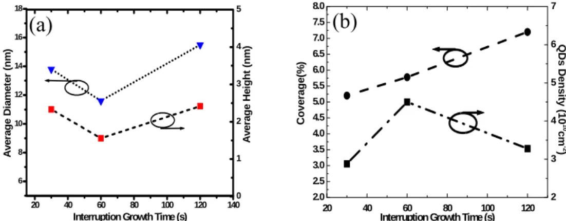
used as the template for InGaN QDs structure (Fig.1(a)). The growth conditions of InGaN QDs were low V/III ratio (~8000) and low growth temperature (660oC). Fig. 1(b) shows the typical surface image of InGaN QDs structure. The QDs density was about 4.5 * 1010 cm-2 with an average lateral size of 20nm and an average height of 2nm. The interruption growth was used to improve the quality of InGaN QDs and the effect of interruption time (tint) has also been
investigated. Our results suggest that the interruption growth can modify the size of InGaN QDs and the emission peak energy. Fig. 2(a) shows the averaged height and diameter of the samples with various interruption times. The mean size (diameter, height) of sample A (tint=30s), B
Fig.2(b) shows the dependence of the coverage above the wetting layer, and QDs density on the interruption time. The coverage increases from 5.2% to 7.2% by increasing tint from 30s to 120s
and the QDs density has a maximum value, 4.5 * 1010 cm-2 at tint=60s. These results implied that
ad-atom surface diffusion effect always exists during the process of interruption growth. The coverage increases from 5.2% to 7.2% was an evidence of the mass transfer from wetting layer; the increase in dot density during the growth interruption 30s<tint<60s was cause by mass transfer
from wetting layer. The decrease in dot density during growth interruption 60s<tint<120s can be
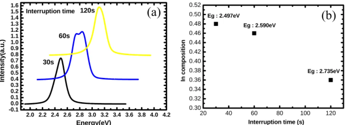
mainly ascribed to the ad-atom surface diffusion, which leads to the enlargement of the largest islands at the cost of the smallest ones due to Ostwald ripening. Fig. 3(a) shows the room temperature PL of these InGaN QDs samples measured using a He-Cd laser as the excitation source. The PL emission peak energy of the InGaN QDs samples is blue-shifted from 2.497eV to 2.735eV as the interruption time increases. We used FEMLAB to calculate the In composition of InGaN QDs. Fig. 3(b) shows the simulation results. It indicated that In composition decreased from 48% to 36% as tint increase from 30s to 120s. It is an evidence of indium desorption which
lead to the decrease of the In composition of the InGaN QDs. In Fig. 4, we plot for all samples the spectrally integrated PL intensity as an Arrhenius plot. From the fitting curve with I ∝exp(EA/kBT), we obtained the activation energy EA for the various sample. For sample A,
EA=63.1meV; for sample B, EA=89.7meV, and for sample C, EA=35.0meV. From the above
results, It indicated that tint=60s is an optima condition for sample B owning smallest QDs size,
largest QDs density and the best optical quality.
Using this technique, indeed, it was feasible for formation of multi layer InGaN QDs structures and applicable for the fabrication of GaN-based light emitting devices.
(a)
(b)
Fig. 1 The surface morphologies of (a) GaN/sapphire template and (b) typical InGaN QDs structure.
(a)
(b)
20 40 60 80 100 120 140 6 8 10 12 14 16 18 0 1 2 3 4 5 A v er ag e Hei g h t ( n m) A v er ag e Di amet er ( n m )Interruption Growth Time (s)
2 3 4 5 6 7 20 40 60 80 100 120 2.0 2.5 3.0 3.5 4.0 4.5 5.0 5.5 6.0 6.5 7.0 7.5 8.0 QD s De n s ity ( 1 0 10 cm -2 ) Co v e ra g e (% )
Interruption Growth Time (s)
Fig. 2 (a) Average diameter and average height, and (b) InGaN QDs density and the coverage in dependence of the interruption time.
II. Fabrication and measurement of InGaN/GaN multiple quantum wells nanorods
1. Fabrication of GaN-based nanorods by self-assembled Ni nano-masks and ICP-RIE dry etching
In this section, we attempted to study the fabrication and μ-PL characterization of Mg-doped GaN nanorods fabricated from a GaN epitaxial film by self-assembled Ni nano-masks and inductively coupled plasma reactive ion etching (ICP-RIE). A large spectral blueshift of the PL peak was observed for the Mg-doped GaN nanorod with respect to the Mg-doped GaN film. As
Fig.3 (a) Photoluminescence spectra of these samples at room temperature under an excitation power of 20mW. (b) Simulation results of In composition of InGaN QDs under various interruption time.
0.00 0.01 0.02 0.03 0.04 0.05 0.06 0.01 0.1 1 In te g ra te d P L In te n s it y (a .u .) 1/T (1/k) tint=30s tint=60s tint=120s
Fig. 4 Arrhenius plots of the integrated PL intensity as a function of temperature.
20 40 60 80 100 120 0.30 0.32 0.34 0.36 0.38 0.40 0.42 0.44 0.46 0.48 0.50 0.52 Eg : 2.735eV Eg : 2.590eV Eg : 2.497eV In co m pos it ion Interruption time (s) 2.0 2.2 2.4 2.6 2.8 3.0 3.2 3.4 3.6 3.8 4.0 4.2 -0.1 0.0 0.1 0.2 0.3 0.4 0.5 0.6 0.7 0.8 0.9 1.0 1.1 1.2 1.3 1.4 1.5 1.6 Interruption time 30s 60s 120s In te n s ity (a .u .) Energy(eV)
(a)
(b)
Fig. 5 SEM images of the etched GaN sample surface morphology for different chamber pressures: (a) 2.5 mTorr, (b) 10 mTorr, (c) 20 mTorr and (d) 30 mTorr at the same Cl2/Ar flow rate of 10/25 sccm, ICP/bias power of 200/200W for 2 min etching time.
Fig. 6 PL peak energy as function of excitation power density. Filled (open) squares represent Mg-doped GaN nanorod (film) while open circles indicate the undoped GaN nanorod.
shown in the SEM image in Fig. 5(a), a uniform etched surface with no nanorod formation was observed at and below the chamber pressure of 2.5 mTorr, and the surface roughness was approximately 1.5 nm. As the chamber pressure was increased to 10 mTorr, GaN nanorods began to form and the density of the nanorods increased as the chamber pressure was further increased to 20 mTorr and 30 mTorr. The nanorods had a near hexagonal structure with a height of approximately 1 mm as estimated from the SEM images shown in Figs. 5 (b) and (c), and about 0.4 mm at 30 mTorr from Fig. 5(d). The variation in the height of the nanorods seems to be related to the etching rate. In our experiment, the etching rate was approximately 3000 _A/min at 2.5 mTorr, and increased to approximately 5000 _A/min at 10 mTorr and 20 mTorr, and then decreased to 1450 _A/min at 30 mTorr. This seems to correspond to the variation in height of the nanorods. At 30 mTorr, as shown in Fig. 5(d), the nanorods formed a two-dimensional array of uniform density. Figure 6 shows high-resolution SEM images of the high-density Mg-doped GaN nanorods. Figure 5(a) shows the top view image of the Mg-doped GaN nanorods, and the density of the nanorods was estimated to be approximately 3 _ 1010 cm_2. Figure 5(b) shows a high-resolution SEM image of the nanorods exhibiting a nanorod diameter of approximately 50 nm. Figure 6 plots the PL emission peak energy as a function of excitation power density for a Mg-doped nanorod, a Mg-doped GaN film and an undoped GaN nanorod. The PL peak energy increases were 125 meV and 67 meV for the Mg-doped nanorod and Mg-doped GaN film respectively as the excitation intensity varied from 12 kW/cm2 to 56 kW/cm2. The corresponding spectral shift between the nanorod and the non-nanorod peaks ranging from 8 meV to 67 meV within the excitation intensity range indicates stronger the power dependence of the Mg-doped GaN nanorod emission. In contrast, the PL emission peak of the undoped GaN nanorod appeared the same in the same excitation range.
2. Optical properties of blue light MQW nanorods
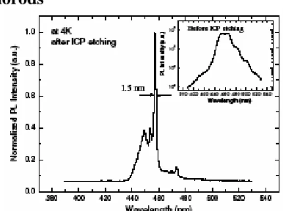
Figure 7 displays a typical SEM image of In0.3Ga0.7N/GaN MQWs nanorods. The nanorods
fabricated by ICP dry etching were almost vertical and straight shape. The nanorods have lengths up to 500 nm and diameters ranging from 60 to 100 nm. Nanorods with diameters less than 55 nm were also observed. About 9~16 nanorods were probed in the μ-PL measurement based on the rod-density of ~ 3 ×10⁸ estimated from fig. 7. A typical PL spectrum of the InGaN/GaN nanorods under an excitation density of 0.9 W/cm2 was measured at 4 K as shown in fig. 8. It consists of several discrete emission peaks whose positions are at 449, 453 and 457 nm respectively. The
Fig. 7 Scanning electron microscopy image of In0.3Ga0.7N/GaN MQWs nanorods.
Fig. 8 PL spectrum of In0.3Ga0.7N /GaN MQWs nanorods.
strong narrow emission peak at 457 nm has a full width at half maximum (FWHM) of about 1.5 nm. The position difference between each peak is estimated to be 4 nm (24 meV). The insert in fig. 8 is the spectrum from the as-grown bulk wafer before the ICP etching, which was measured at the same condition for the nanorods. It shows a typical InGaN/GaN MQWs spectrum with a FWHM of about 26.5 nm and an undulation behavior which is probably due to the Fabry-Perot interferences within the epitaxial layers. Indeed, the fabrication of nanorods structure from the In0.3Ga0.7N/GaN MQWs bulk wafer does exactly show the different behavior than the typical PL
emission spectra of bulk MQWs. This could be due to the decrease of in-homogeneous broadening in wells of nanorods. Figure 9 shows a series of spectra record at different excitation densities between 0.9 and 10.1 W/cm2 for the In0.3Ga0.7N/GaN MQWs nanorods at 4K. Under
low excitation densities, the e1-h1 peak at 457 nm is dominant. However, with increasing excitation density, the intensity of peak on the high-energy side of the e1-h1 peak increases. Finally, this peak at 453 nm becomes dominant over the e1-h1 emission.
3. Optical properties of green MQW nanorods
By following the above method, by choosing the appropriate initial Ni thickness, annealing temperature, and annealing time, we can fabricate a self-assembled nanosize Ni masks. In this section, we studied the optical properties of InGaN/GaN MQW green nanorod structures. The optical properties have not been fully studied yet since the higher In content in the c-plane MQW could result in lower emission efficiency due to the strong quantum confined Stark effect. In this part, we present the results of enhanced emission intensity properties of InGaN/GaN MQW green emission nanorods and analyze the dominant enhancement mechanism using temperature-dependent PL and time-resolved photoluminescence (TRPL).
Fig. 9 Excitation power dependent photoluminescence spectra of In0.3Ga0.7N/GaN MQWs nanorods.
Fig. 10(a) An Arrhenius plot of the integrated PL intensity obtained from the In0.3Ga0.7N/GaN MQW
Fig. 10(b) TRPL lifetime curves of the In0.3Ga0.7N/GaN MQW as-grown and green emission
Figure 10(a) shows an Arrhenius plot of the integrated PL intensity obtained from the In0.3Ga0.7N/GaN MQW active layer emission of the as-grown sample and the nanorod sample
over the temperature range from 20 to 300 K. The results indicate that the PL intensity of the nanorods is stronger than that of the as-grown sample by a factor of approximately 3.5 at room temperature. Such large emission enhancement could result from improvement either in internal quantum efficiency or external extraction efficiency. The temperature-dependent data of figure 10(a) were fitted with the following formula:
IT = I0/[1+A exp (−Ea/kT )+B exp (−Eb/kT)]
where IT , I0 are the integrated PL intensity for T and 0 K, A and B are constants, k is the
Boltzmann constant, T is the temperature, Ea is the activation energy for PL quenching, and Eb is generally associated to the free exciton binding energy. The energy Eb of the as-grown and nanorod samples was approximately 6.2 and 7.8 meV, respectively, which was similar to values in the previous report. However, the activation energy Ea of as-grown and nanorod samples was 35 and 79 meV, respectively. Though the high surface ratio around the periphery of the nanorods could provide many non-radiative recombination paths, the larger activation energy of the nanorods obtained seems to suggest that there are higher potential barriers in the nanorods for carriers, where they could easily localize in the effective potential minima of the nanorod structures.
Figure 10(b) shows the carrier lifetime from the as-grown and nanorod samples measured by TRPL at 10 and 300 K respectively. Since a purely radiative recombination at T = 10 K can be assumed, the radiative lifetime of the nanorod sample is similar to that of the as-grown sample, which is approximately 54 ns, indicating that the radiative recombination process for both samples is similar and the internal field reduction in the nanorods sample plays a minimal role in the emission enhancement. As the temperature increased to 300 K, the carrier lifetimes were further shortened to 8.7 and 16.5 ns for the nanorod and as-grown samples due to the increase of the non-radiative recombination rate in the nanorod structures. The relatively larger non-radiative recombination rate at room temperature for the nanorod sample was probably due to the increasing surface recombination around the periphery of the nanorod. Generally, reduction of the internal PZ field facilitates a better wavefunction overlapping of electrons and holes in the green emission nanorod MQWs that could result in the increase of the emission efficiency and enhancement in the PL emission intensity of the nanorods. However, the PRTL measurement results reveal that the reduction of the internal PZ field could not be large enough to enhance the radiative recombination process in the green emission nanorods. As a result, the internal quantum efficiency of the nanorod sample at room temperature could not be improved, indicating that the PL intensity enhancement observed from the nanorod sample could result from the increased emission surface of the nanorod structure.
4. Fabrication and characteristics of AN-based nanorods LED
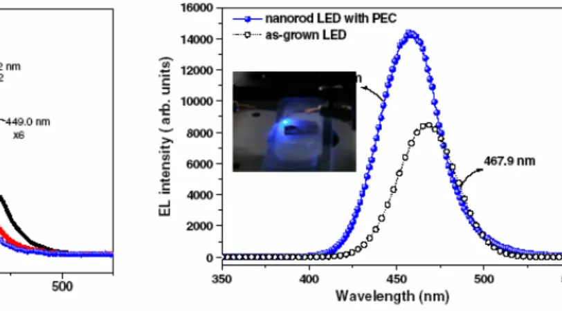
In this section, we based on the nanorod fabrication technique continuously and introduced a novel method combining ICP-RIE and the PEC wet oxidation process with self-assembled Ni metal islands to fabricate InGaN/GaN nanorod LEDs. Figure 11shows the normalized PL spectrum of the as-grown LED sample, and nanorod
LED samples made with and without the PEC process measured at room temperature. A HeCd laser (325 nm) was used with an excitation power of 25 mW and the power density of 1.5 Wcm−2. The PL emission peaks of the
InGaN/GaN active layer were bserved at 449.0, 445.2 and 440.4 nm for as-grown samples, and nanorods samples made without and with the PEC oxidation process, respectively. The PL peak intensities of InGaN/GaN MQW active layers in nanorods made with and without the PEC oxidation process were enhanced by factors of approximately six and five times compared with as-grown LED samples. The blue-shift phenomena were observed for both the nanorod LED samples made with and without the PEC oxidation process, and the blue-shift values were 3.8 nm (20 meV) and 8.6 nm (50 meV), respectively. The blue shift might be caused by the partial reduction of the piezoelectric field by the strain release in the nanorod structures Figure 12shows the room-temperature EL spectrum of the as-grown LED and nanorod LED samples made with the PEC oxidation process at an injection current of 1 mA. The inset of figure 12shows the emission image of the InGaN/GaN MQW nanorod LED. It shows that the PEC oxidation process can effectively form oxidation layers to isolate the nanorods and facilitate contact formation. The EL intensity of the nanorod LED made with the PEC process was about 1.76 times that of the as-grown LED
III. Fabrication and characteristics of the micro-cavity
1. Successfully improved the reflectivity of GaN/AlN DBR reaches about 97% by the
insertion of the nano-scaled super-lattice.
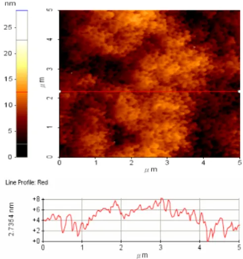
The crack-free distributed Bragg reflectors (DBR) structure was successfully grown. Insertion of three sets of AlN/GaN superlattice is shown to significantly reduce the biaxial tensile strain, thereby resulting 20 pairs about 1.8 μm-thick, crack free high-reflectivity AlN/GaN distributed Bragg reflectors. The schematic structure of the grown DBR is shown in Fig.13. The surface also was measured by AFM shown in Fig. 14. The surface roughness Ra of this DBR
sample is 2.5 nm and the grain size is 0.15 μm. The line profile shows the crack free. The cross-sectional TEM image of superlattice insertion was shown in Fig. 15. Reflectivity spectra of AlN/GaN DBR with three superlattice insertions were shown in Fig. 16. To study the distribution of reflectivity, we measured on three areas with 2mm diameter taken across the 2-inch wafer in the direction of a cross. Fig. 16 shows the reflectance spectra of three areas A, B and C, which are located in order from the center of a wafer to the radius direction. At area A, the peak reflectivity of 97% was obtained at wavelength of 399 nm and a stopband of 14 nm, and at area B, 97% at 405 nm. This peak wavelength was in good agreement with the required value. At area C, the
Figure 11. Normalized PL intensity spectra for as-grown LED and nanorod LEDs made with and without the PEC process at room temperature.
Figure 12. The EL intensity spectra for as-grown LED and nanorod LED made with the PEC process at room temperature. The inset shows a photographic image of the blue emission from an InGaN/GaN MQW nanorod LED at 1 mA dc current.
peak wavelength was 432 nm. This was caused by the difference of growth rate due to the temperature distribution of heater. Now the full vertical cavity surface emitting laser structure with crack-free DBR has been grown and fabrication of devices is in process.
2. Successfully achieved laser operation by an optical excitation of the micro-cavity structure with hybrid mirrors.
The structure of the GaN-based VCSEL was grown in a vertical-type MOCVD system (EMCORE D-75). The polished optical-grade C-face (0001) 2-inch-diameter sapphire was used as substrate for the epitaxial growth of the VCSEL structure. The VCSEL structure composed of a 3λ cavity, a 20 pairs AlN/GaN DBR as bottom mirror and an eight pairs Ta2O5/SiO2 dielectric
mirror as the top DBR reflector. The schematic diagram of the full structure is shown in figure 17. During these processes, the peak reflectance of the AlN/GaN DBR structure and the Ta2O5/SiO2
dielectric mirror were 97.5% and 94% at 450nm, respectively. Figure 18 shows the laser emission intensity as a function of pumping energy at room temperature condition. A distinct threshold characteristic was observed at the threshold pumping energy (Eth) of about 1.5μJ corresponding
to an energy density of 53mJ/cm2. The laser intensity increases linearly with the energy level beyond the threshold energy. Figure 19 shows the variation of emission spectrum with the increasing pumping energy. A dominant laser emission line at 448nm appears above the threshold pumping energy. The laser emission spectral linewidth reduces as the pumping energy above the
Fig. 13 Schematic structure of 20-pair Anlagen DBR with three super lattice insertions.
Fig. 14 The image of surface of DBR sample
Fig. 15 Cross-sectional TEM image of DBR structure. Fig. 16 Reflectivity spectra of the 20 pairs DBR with three AlN/GaN SLs measured at room temperature as a function of wavelength taken across the 2-inch wafer.
300 400 500 0 20 40 60 80 100 A B C Inte ns ity (a .u) Wavelength(nm) CBA 97% sapphire 5 pairs AlN/GaN 5 pairs AlN/GaN 5 pairs AlN/GaN 5 pairs AlN/GaN GaN-1μm GaN AlN/GaN
threshold energy and approaches 0.25nm at the pumping energy of 2.52Eth.
3. Successfully fabricated a micro-cavity with high reflectivity DBR using laser lift-off technique
The epitaxial structure of the GaN-based VCSEL was first grown on a (0001)-oriented sapphire substrate by metal organic chemical vapor deposition system. The structure consists of a 30-nm nucleation layer, 4-μm undoped GaN, a multiple quantum-well composed of 10 periods of 5-nm GaN barrier and 3-nm In0.1Ga0.9N well, and 200 nm undoped GaN. Then a dielectric DBR
consisting of 6 pairs of SiO2 and TiO2 was evaporated on the top of the grown structure to form a
SiO2/TiO2 DBR/InGaN MQW/GaN/sapphire structure. The structure has a peak reflectivity of
99.5% at 414 nm. Then, an array of disk-like SiO2/TiO2 DBR mesas with 60 μm in diameter was
formed. The patterned SiO2/TiO2 DBR/InGaN MQW/GaN/sapphire structure was then mounted
onto a host fused silica substrate. The mounted sample was then subjected to a laser lift-off process. Finally, the second DBR consisting of 8 pairs of SiO2 and Ta2O5 was deposited on the
top of the polished GaN surface. The reflectivity of the SiO2/Ta2O5 DBR at 414 nm is 97%. The
complete structure of the GaN VCSEL with two dielectric DBRs is shown in Fig. 20(a). 0 1 2 3 4 5 0 2000 4000 6000 8000 10000 Em is s io n In te n s ity (a.u .)
Excitation Energy (μJ/pulse)
430 440 450 460 470 0.25nm 2.52 E th 1.64 Eth 1.38 E th 0.75 E th 1.13 Eth In te n s it y (a .u .) Wavelength (nm) 8 pairs Ta2O5/SiO2 25 pairs AlN/GaN n-GaN Sapphire p-GaN MQWs
FIG.17. The schematic diagram of the overall structure.
FIG.18. The light output intensity as a function of the pumping energy at room temperature.
FIG.19. The variation of laser emission spectrum with the increasing pumping energy.
4. Successfully optically pumped InGaN-MQW VCSELs with two high –reflectivity dielectric DBRs
The structure above was successfully optically pumped and achieved lasing action at room temperature. The setup of optical pumping is shown in the figure 20(a). Figure 20(b) shows the laser emission intensity as a function of pumping energy at room temperature condition. A clear evidence of threshold condition occurs at pumping energy of 270 nJ corresponding to an energy density of 21.5 mJ/cm2. The laser intensity increases linearly with the pumping energy level beyond the threshold energy.
Figure 21(a) shows the evolution of the VCSEL emission spectrum with the pumping energy at room temperature. At below threshold pumping energy, the spontaneous emission spectrum shows a multiple cavity modes with a mode spacing of about 7 nm and a linewidth of about 0.8 nm. This mode spacing corresponds to a cavity length of 4 μm which is nearly equal to the thickness of the GaN layer inside the cavity. The cavity quality factor (Q factor) estimated from the linewidth is about 518. As the pumping energy increases above the threshold, a dominant laser emission line appears at 414 nm with a narrow linewidth of about 0.25 nm. Figure 21(b) shows the 3-D isometric plot of the spatial intensity distribution of the laser beam.
0.25Eth Eth 1.13Eth 0.25 nm 390 395 400 405 410 415 420 425 430 435 440 0.0 0.5 1.0 1.5 2.0 2.5 3.0 3.5 4.0 4.5 5.0 E m is s io n in te n s ity (a .u .) Wavelength (nm)
Fig. 21(a) Fig. 21(b)
host substrate InGaN patterned SiO2/TiO2 DBR SiO2/Ta2O5 pumping laser VCSEL spectra
VCSEL emission patterns
40×
15×
Fig. 20(a) The setup for optical pumping of the GaN VCSEL with two dielectric DBRs. (b) Laser emission intensity as a function of the pumping energy operated at room temperature. The threshold pumping energy is about 270 nJ.
Fig. 20(a) Fig. 20(b)
100 150 200 250 300 350 0 10 20 30 40 50 E m ission int e ns it y ( a .u .)
368 370 372 374 376 0 1000 2000 3000 4000 15.31 MW/cm2 11.13 MW/cm2 9.03 MW/cm2 Emiss ion intensity (AU) Wavelength(nm) III. Fabrication and characteristics of the micro-cavity
1. GaN quantum whispering gallery light emitting laser formed by photo-enhanced wet
chemical oxidation and crystallographic etching
Combined with photo-enhanced wet chemical oxidation and crystallographic etching, we demonstrated GaN microcavities with various geometries, including Fabry-Perot cavity with vertical mirror facets of (10-10), faceted hexagon, and cylindrical cavities with smooth vertical sidewalls. Stimulated emission due to resonance with whispering gallery (WG) modes in the above cavities was observed under optical pumping with a 266nm Nd:YAG laser. Increase of the mode spacing and suppression of the side mode emission intensity were observed with device size as small as to 2μm.
As shown in Fig.22, the stimulated emission at ~ 372nm was observed at room temperature in the 5μm size hexagonal micro-facet cavity with a pumping threshold of~ 10MW/cm2 and full
width at half maximum (FWHM) ~0.9nm. Note the integrated peak intensity in the stimulated emission regime increases roughly with a relation Istimu ~Ipump2, revealing a dominant mechanism
by electron-hole plasma scattering, i.e., |<ΦeΦh|p| ΦeΦh>|2 Compared with a Fabry-Parot
cavity made of the same (10-10) etched facets and optical length, the lasing threshold in the former is lower by 20%.
2. Gallium nitride microcavities formed by photoenhanced wet oxidation
Fig. 21(a). Emission spectra from the GaN-VCSEL at various pumping energy. (b) shows the 3-D isometric plot of the spatial intensity distribution of the laser beam.
101 103 E m is s ion In te ns it y Pth = 10MW/cm2 I~Ip0.7 I~Ip2.3 Pumping Intesnsity (MW/cm2)
Fig. 22(a) SEM image of 5 μm hexagonal microcavity, (b) the PL spectrum exhibits mode spacing ~ 0.6 nm and (c) pumping threshold ~10MW/cm2. The emission intensity increases with the relation I~I
Since the oxidized GaN layer can be dissolved in dilute acid or base solutions, a combination of the repeated photoenhanced wet oxidation and dissolution (etching) can thus be a promising route for the realization of GaN microcavities. Illustrated in Fig. 22 are the SEM micrographs showing the top view of GaN hexagonal microcavities formed by dissolving a 1-μm-thick oxidized GaN structure in (a) dilute CH3COOH solution and (b) molten KOH at 180 °C for 1 min,
respectively. The magnified cross-sectional SEM micrograph in the inset of Fig. 22(a) indicates a smooth sidewall can be retained by this proposed method. Except for a partial removal of the Ti mask by a short time immersion in molten KOH, no apparent difference can be found on the sidewall smoothness with respect to the choice of oxide dissolving solutions used in Figs. 22(a) and 22(b). These observations elucidate a principle to retain smooth GaN facets by slowly photo-oxidizing the nonpolar GaN planes at a rate much less than 1 nm/min. In comparison, for the polar (0001) GaN plane where the photoenhanced oxidation rate can proceed at a rate of 1
nm/min or higher, a wavy oxidized surface can be observed due to a localized, nonuniform distribution of the photoexcited carriers and reactants. Illustrated in Fig. 22(c) is one such hexagon of 2 μm radius, showing a smooth, vertical sidewall and inclined (1-103 GaN facets near
the cavity pedestal.
Illustrated in Fig. 23 are the cavity size dependent luminescence spectra of GaN hexagons, revealing the characteristic peaks of WG modes in resonance with the GaN emission spectrum. Note a mode spacing of 0.74, 1.1, and 1.5 nm, respectively, are clearly discernible with a reduced hexagon radius of R=2, 3, and 5 μm at a constant pump intensity Ip~4 MW/cm2. These data agree well with a theoretical analysis by enforcing an optical path _shown in the inset of Fig. 23 to have a total phase shift equal to an integer multiple of 2π and thus to ensure total internal reflections inside the GaN microcavities.
(五) Reference
[1] R. G. Hulet, E. S. Hilfer, and D. Kleppner, Phys. Rev. Lett. 55, 2137 (1985).
[2] P. Goy, J. M. Raimond, M. Gross, and S. Haroche, Phys. Rev. Lett. 50, 1903 (1983). [3] E. Kapon,D. M. Hwang, M. Walther, R. Bhat, and N. G. Stoffel, Surf. Sci. 267, 593
(1992)
[4] C. Weisbuch and B. Vinter, Quantum Semiconductor Structures (Academic, San Diego, CA, 1991)
[5] D. L. Huffaker, O. Baklenov, L. A. Graham, B. G. Streetman, and D. G. Deppe, Appl. Phys. Lett. 70, 2356 (1997)
(六) 與國外學術合作
Fig. 22 Top view of SEM micrograph showing GaN hexagonal cavities after dissolving the PEC-grown oxide in (a) CH3COOH and (b) molten KOH. Inset: magnified cross-sectional SEM micrograph revealing an optically smooth sidewall in (a). (c) Cross-sectional SEM micrograph of a typical hexagonal GaN cavity to be used in the micro-photoluminescence study. The hexagon side length is 2 μm.
Fig. 23. Cavity size dependent emission spectra of GaN hexagons with radius R=5, 3, and 2μm measured at an intensity I~4 MW/cm2 of 266 nm YAG laser. The spectra have been vertically shifted for comparison.
Prof. S. C. Wang, the leader of this three year project, already achieved an agreement with Prof. Yamamoto of Stanford University on cooperation of developing next generation GaN single photon emitter. One graduate student and Prof. Lu have been visited his lab for few months research to conduct preliminary and measurement experiment. The experience gained from Prof. Yamamoto on the GaAs-based QD microcavity device will be very useful for this effort and will ensure the successful outcome of this experiment. Besides, the research group had collaborated with Prof. K. Iga of Tokyo Institute of Technology, who is the first one to demonstrate the VCSEL structure, for GaN blue VCSEL. We had also collaborated with Prof. S.L. Chuang of UIUC, who got the excellent efforts of slow light in fiber communication, for the fabrication and performance measurement of VCSEL.
(七) 計畫成果自評 本計畫第一年預定目標如下: 1. 建立具備光學微共振腔之低維氮化鎵量子點、柱結構生長與製作,包括氮化鎵DBR反射 膜與量子點之磊晶成長研究。 2. 氮化鎵面射型雷射結構之製程研究。 3. 以自組式光致氧化技術,生長二維奈米尺度之AlGaO、InGaO/GaN 量子柱結構。 本計畫第二年預定目標如下: 1. 光學微共振腔之低維氮化鎵量子點、柱結構生長與製作,包括氮化鎵 DBR 反射膜與量子 點之磊晶成長及其發光元件製作之研究。 2. 建立光學微共振腔結構之物理性質量測與分析。 3. 氮化鎵面射型雷射結構之光學與電性特性研究。 4. 生長 AlGaO、InGaO 等光致自然氧化薄膜技術,研究其對於光學微型共振腔之表面保護、 光學係數匹配,以及對於光學增益係數之提昇。 本計畫第三年預定目標如下: 1. 製作氮化鎵基量子點與面射型雷射元件 2. 分析研究量子侷限可控制光子輻射現象 3. 與史丹佛大學 Yamamoto 教授合作展示可控制光子輻射 在相關研究人員包括所有計畫共同主持人、博士後研究員、數十位博碩士生在這三年 來的努力之下,所完成的成果相當豐碩,包括成功利用有機化學氣相沈積系統成長高密度 氮化銦鎵量子點、利用乾式蝕刻方式以及自組成奈米遮罩蝕刻出直徑約100 nm 的奈米柱並 研究其物理性質(其中奈米柱裡包含多重量子井(發光層)),並對其發光機制與光學特性 作完整的探討、利用奈米尺寸之超晶格插入成長出高反射率無裂縫之AlN/GaN DBR 多層 反射膜、氮化鎵微共振腔發光元件之製造與達到光激發面射型雷射、以及利用光致氧化與 蝕刻製作出氮化鎵共振腔並達雷射輸出,此與原計畫所預定的目標已幾乎相符,其中面射 型雷射的成功製作更可說明目前的研究成果與能力已能與世界許多一流之研究團體相提並 論,本研究團隊再奈米尺寸下的元件製作包括兩種不同反射鏡之面射型雷射、奈米柱元件 和利用光電化學氧化製作之微共振腔的研究成果以發表總計數十篇的國際期刊論文,應邀
出席數十場國際研討會並發表論文,在計畫期間所培養出來之碩博士生超過三十名,對於 過內在學術上以及產業界均有相當大的助益。同時,本團隊和史丹佛大學Yamamoto 教授 的研究團隊在過去三年內進行相當密切的合作,除了有多位博士生到該實驗室進行實驗 外,本團隊之盧廷昌亦到該實驗室進行數月的短期研究,對於本團隊在這方面的研究有很 大的助益。對氮化鎵面射型雷射的微共振腔結構,以及利用本團隊之有機化學氣相沉積系 統成長之量子點的量子侷限現象,和利用本研究團隊研發之奈米柱結構在特性上做相當深 入的研究。 (八) 研究成果紀錄----附件一
「氮化鎵介觀尺度下量子局限結構之光子幅射可控性研究」研究成
果紀錄
總主持人:王興宗 服務機關:國立交通大學光電工程研究所
共同主持人:孟心飛,彭隆瀚,林恭如,郭浩中
計畫執行期限:92/08/01~96/07/31
填表日期: 研究成果 92 年度 93 年度 94 年度 95 年度 總計 國內(篇數) 1 0 0 0 1 期刊論文 國際(篇數) 10 17 10 27 64 會議論文 國內外(篇數) 0 5 16 23 44 專利(案數) 0 2 1(申請中) 3(申請中) 6 智慧財產權 技術移轉(件數) 0 0 0 0 0 博士生培育(人數) 4 4 3 3 14 人才培育 碩士生培育(人數) 7 6 5 5 23 註:人才培育人數請勿重複計算 附件一發表之期刊論文列表
註:請按發表時間先後順序填寫,每篇請依作者姓名(主要作者請以粗體字標示)、期刊年 份、題目、期刊名稱、起迄頁數、期刊資料庫類別(SCI、SSCI、EI…)之順序填寫。 例:1.Chen YJ, Chen PJ, Lee MC, Yeh SH, Hsu MT, and Lin CH. (2002) Chromosomal analysis
of non-malignant liver tumors by comparative genomic hybridization. Genes
Chromosomes and Cancer 35:2 (SCI)
國際期刊論文: Journal paper ﹡2003:
1. HC Kuo, YS Chang, FY Lai, TH Hsueh, Laih LH ,SC Wang, “High-speed modulation of 850 nm InGaAsP/InGaP strain-compensated VCSELs,” Electronics Letters 39 (14): 1051-1053 JUL 10 (2003) (SCI: 1.016)王興宗
2. LB Chang, SC Wang, AH Kung,“Numerical analysis of fifth-harmonic conversion of low-power pulsed Nd : YAG laser with resonance of second harmonic,” Japanese Journal of Applied Physics 42 (7A): 4318-4324 JUL (2003) (SCI: 1.142) 王興宗 3. CF Chu, CC Yu, HC Cheng, CF Lin, SC Wang,“Comparison of p-side down and p-side
up GaN light-emitting diodes fabricated by laser lift-off,” Japanese Journal of Applied Physics 42 (2B): L147-L150 FEB 15 (2003) (SCI: 1.142) 王興宗
4. TC Lu, JY Tsai, JT Chu, YS Chang, SC Wang, “InP/InGaAlAs distributed Bragg reflectors grown by low-pressure metal organic chemical vapor deposition,” Journal of Cryatal Growth 250 (3-4): 305-312 APR (2003) (SCI: 1.707) 郭浩中,王興宗 5. Chen CC, Hsueh TH, Ting YS, Chi GC, Chang CA, Wang SC, “Thermal annealing
effects on the optical gain of InGaN/GaN quantum well structures,” Solid-State Electronics 47 (3): 575-578 MAR (2003) (SCI: 1.159)王興宗
6. CC Yu, CF Chu, JY Tsai, HW Huang, TH Hsueh, CF Lin, SC Wang, “Gallium nitride nanorods fabricated by inductively coupled plasma reactive ion etching,” Japanese Journal of Applied Physics 41 (8B): L910-L912 AUG 15 (2002) (SCI: 1.142) 王興宗 7. JL He, CK Lee, JYJ Huang, SC Wang, CL Pan, KF Huang ,“Diode-pumped passively mode-locked multiwatt Nd : GdVO4 laser with a saturable Bragg reflector,” Applied Optics 42 (27): 5496-5499 SEP 20 (2003) (SCI: 1.717) 王興宗
8. FI Lai, TH Hsueh, YH Chang, WC Shu, LH Lai, HC Kuo, SC Wang ,“Performance of 850 nm AlGaAs/GaAs implanted VCSELs utilizing silicon implantation induced disordering,” Solid-State Electronics 47 (10): 1805-1809 OCT (2003) (SCI: 1.159) 郭 浩中、王興宗
9. JY Tsai, TC Lu, SC Wang,“High reflectivity distributed Bragg reflectors for 1.55 mu m VCSELs using InP/airgap” Solid-State Electronics 47 (10): 1825-1828 OCT (2003) (SCI: 1.159) 郭浩中、王興宗
10. TH Hsueh, HC Kuo, FI Lai, LH Laih, SC Wang “High-speed characteristics of large-area single-transverse-mode vertical-cavity surface-emitting lasers” Electronics
Letters 39 (21): 1519-1521 OCT 16 (2003) (SCI: 1.016) 王興宗
﹡2004:
1. J. T. Chu, H. W. Huang, C. C. Kao, W. D. Liang, F. I. Lai, C. F. Chu, H.C. Kuo and Shing-Chung Wang, “Study of GaN light-emitting diodes fabricated by laser lift-off technique”, Journal of Applied Physics 95 (8): 3916-3922 Apr 15 (2004) (SCI:2.255)
郭浩中,王興宗
2. C. C. Kao, H. W. Huang, J. Y. Tsai, C. C. Lu, C. F. Lin, H. C. Kuo, and S. C. Wang, “Study of dry etching for GaN and InGaN-based laser structure using inductively coupled plasma reactive ion etching,” Materials Science and Engineering B107, 283-288(2004) (SCI: 0.924) 郭浩中,王興宗
3. H. C. Kuo, Y. S. Chang, F. Y. Lai, T. H. Hseuh, L. T. Chu, L. H. Laih and S. C. Wang, “High speed performance of 850 nm silicon-implanted AlGaAs/GaAs vertical cavity emitting lasers,” Solid-State Electronics, 48, 483-485(2004) (SCI: 1.159) 郭浩中,王 興宗
4. C.F. Chu, F.I. Lai, J.T. Chu, C.C.Yu, C.F. Lin, H.C. Kuo, and S. C. Wang, “Study of GaN Light Emitting Diodes Fabricated by Laser Lift-off Technique,” J. Applied Phys., 95, 3916-3922(2004) (SCI:2.255) 郭浩中,王興宗
5. H. H. Yao, C. F. Lin, H. C. Kuo and S. C. Wang, “MOCVD growth of AlN/GaN DBR structures under various ambient conditions,” J. of Crystal Growth, 262, 151-156(2004) (SCI: 1.707) 郭浩中,王興宗
6. C. F. Lin, H. H. Yao, J. W. Lu, Y. L. Hsieh, H. C. Kuo, and S. C. Wang,” Characteristics of stable emission GaN-based resonant cavity light emitting diodes,” J. Crystal Growth, 261 , 359-363(2004) (SCI: 1.707) 郭浩中,王興宗
7. H. W. Huang, C. C. Kao, J. T. Chu, C. C. Yu, C. F. Lin, H. C. Kuo and S. C. Wang, “Investigation of GaN LEDs with Be-implanted Mg-doped GaN layer,” Materials Science & Engineering, B113, 19–23(2004) (SCI: 0.924) 郭浩中,王興宗
8. H. C. Kuo, S. C. Wang, “MOCVD growht of highly strained InGaAs:
Sb-GaAs-GaAsP Quantum Well Vertical Cavity Surface Emitting Lasers with 1.27 μm emission”, Journal of Crystal Growth, 272, 538(2004) (SCI: 1.707) 郭浩中,王興宗
9. T.C. Lu, W. C. Hsu, Y. S. Chang, H. C. Kuo and S.C. Wang, “Spectrally resolved
spontaneous emission patterns of oxide-confined vertical-cavity surface-emitting lasers”, J. Appl. Phys. 96, 5992(2004) (SCI:2.255) 盧廷昌,郭浩中,王興宗
10. F.I. Lai, Y.H. Chang, T.H. Hsueh, H.W. Huang, L.H. Laih, H.C. Kuo, S.C. Wang and T.C. Gung, “Improvement of kink characteristics performance of GaAs VCSEL with a
indium-tin-oxide top transparent overcoating” Materials Science and Engineering B, 113, 203, (2004) (SCI: 0.924) 郭浩中,王興宗
11. H. W. Huang, C. C. Kao, T. H. Hsueh, C. C. Yu, C. F. Ling, J. T. Chu, H. C. Kuo, S. C. Wang, “Fabrication of GaN-based nanorod light emitting diodes using self-assemble nickel nano-mask and inductively coupled plasma, ” Materials Science & Engineering B, 113, 125(2004) (SCI: 0.924) 盧廷昌,郭浩中,王興宗
12. Y. A. Chang, H. C. Kuo, Y. H. Chang, S. C. Wang, “Simulation of 1300-nm In0.4Ga0.6As0.986N0.014/GaAsxN1-x quantum-well lasers with various GaAsxN1-x strain compensated barriers, ” Optics Communications, 241,195(2004) 1/2 (SCI: 1.48) 郭浩 中,王興宗
13. Y.H. Chang, H. C. Kuo, F.I. Lai, Y.A. Chang, C. Y. Lu, L. H. Laih, and S. C. Wang , “Fabrication and Characteristics of High-Speed Oxide-Confined VCSELs Using InGaAsP–InGaP Strain-Compensated MQWs “, IEEE J. of Light Wave Technologies, 22, 2828 (2004) (SCI: 2.824) 郭浩中,王興宗
14. F. I Lai, T. H. Hsueh, Y. H. Chang, H. C. Kuo, S C Wang, L. H. Laih, C. P. Song, H. P. Yang, “10 Gb/s single-mode vertical-cavity surface-emitting laser with large aperture and oxygen implantation, “Semiconductor Science and Technology, 19(8), L86(2004) (SCI: 1.586) 郭浩中,王興宗
15. Y. H. Chang, Fang-I Lai, C Y Lu, H C Kuo, H. C. Yu, C. P. Sung, H. P. Yang, S C
Wang, “High-speed (>10 Gbps) 850 nm oxide-confined vertical cavity surface
emitting lasers (VCSELs) with a planar process and reduced parasitic capacitance,” Semiconductor Science and Technology, 19(7), L74(2004) (SCI: 1.586) 郭浩中,王興 宗
16. L. H. Laih, H. C. Kuo, G. R. Lin; L. W. Laih, S. C. Wang, “As+ implanted AlGaAs
oxide-confined VCSEL with enhanced oxidation rate and high performance uniformity,” IEEE Photonic Technology Letter, 16(6), 1423(2004) 1/2 (SCI: 2.552) 郭 浩中,王興宗
17. H. W. Huang, C. C. Kao, J. Y. Tsai, C. C. Yu, C. F. Chu, J. Y. Lee, S. Y. Kuo, C. F. Lin, H. C. Kuo and S. C. Wang, “Effect of rapid thermal annealing on beryllium implanted p-type GaN” Material Sciences & Engineering B-Solid State Materials for Advanced Technology 107(3), 237, (2004) (SCI: 0.924) 郭浩中,王興宗
﹡2005:
1. Tze-An Liu, Gong-Ru Lin, Yen-Chi Lee, and Shing-Chung Wang, Masahiko-Hua Tani, Hsiao-Hua Wu, Ci-Ling Pan, “Dark current and trailing-edge suppression in ultrafast photoconductive switches and terahertz spiral antennas fabricated on multienergy arsenic-ion-implanted GaAs”, Journal of applied physics, Vol. 98, 137111( 2005) (SCI;
2. T. H. Hsueh, H. W. Huang, C. C. Kao, Y. H. Chang, M-C O. Yang, H. C. Kuo and S. C.
Wang, “Characterizaion of InGaN/GaN Multiple Quantum Well Nanorods Fabricated by
Plasma Etching with Self-Assembled Nickel Metal Nanomasks,” Japanese Journal of Applied Physics, vol.44, 4B, 2661 (2005) (SCI: 1.142). 郭浩中,王興宗
3. Y. H. Chang, T. H. Hsueh, F. I. Lai, C. W. Chang, C. C. Yu, H. W. Huanf, C. F. Len, H. C.
Kuo, and S. C. Wang, “Fabrication and Micro-photoluminescence Investigation of
Mg-Doped Gallium Nitride Nanorods,” Japanese Journal of Applied Physics, vol. 44, 4B, 657 (2005) (SCI: 1.142). 郭浩中,王興宗
4. T. H. Hsueh, H.W. Huang, F. I. Lai, J. K. Sheu, Y. H. Chang, H. C. Kuo, and S. C. Wang (SCI), “ Photoluminescence from In0.3Ga0.7N/GaN multiple-quantum-well nanorods,” Nanotechnology, vol. 16, 448 (2005) (SCI: 3.322). 郭浩中,王興宗
5. T. H. Hsueh, J. K. Sheu, F. I. Lai, C. C. Kao, J. Y. Chu, H. C. Kuo, S. C. Wang, “ Light extraction in InGaN micro-hole array light emitting diodes” IEEE Photonics Technology Letters, vol. 17, 6, ??? (2005) (SCI: 2.552). 郭浩中,王興宗
6. H. W. Huang, C. C. Kao, H. C. Kuo and S. C. Wang (2005), “Improvement of InGaN/GaN Light Emitting Diode performance nano-roughened P-GaN Surface” IEEE Photonics Technology Lett., vol. 17, 983 (2005) (SCI: 2.552). 郭浩中,王興宗
7. Jung-Tang Chu, Hung-Wen Huang, Chih-Chiang Kao, Wen-Deng Liang, Fang-I Lai, Chen-Fu Chu, Hao-Chung Kuo and Shing-Chung Wang, “Fabrication of large-area GaN based light-emitting-diodes on Cu substrate” Japanese Journal of Applied Physics, vol. 44, 2509 (2005) (SCI: 1.142). 郭浩中,王興宗
8. Chih-Chiang Kao, Y. C. Peng, H. H. Yao, J. Y. Tsai, Y. H. Chang, J. T. Chu, H. W. Huang, T. T. Kao, T. C. Lu, H. C. Kuo and S. C. Wang, “Fabrication and performance of blue GaN-based vertical-cavity surface emitting laser employing AlN/GaN and Ta2O5/SiO2 distributed bragg reflector” Appl. Phys. Lett, Vol. 87, 181105 (2005) (SCI: 4.308). 郭浩中,王興宗
9. L.-H. Peng, C.-Y. Lu, W.-H. Wu, and S.-L. Wang, “Gallium Nitride microcavities formed by photoenhanced wet oxidation”, Appl. Phys. Lett., Vol87, 161902, (2005) (SCI:
4.308) 彭隆瀚
10. Tao-Hung Hsueh, Jinn-Kong Sheu, Hung-Wen Huang, Ya-Hsien Chang, Miao-Chia OU-Yang, Hao-Chung Kuo and Shing-Chung Wang,” Fabrication and Characterization of In0.25Ga0.75N/GaN Multiple Quantum Wells Embedded in Nanorods ”,Journal of
Applied Physics,Vol.44, 7723 (2005) (SCI:2.255) 郭浩中,王興宗
﹡2006:
1. S.Y. Kuo, W. C. Chen, F. I. Lai , C.P. Cheng , H.C. Kuo , S. C. Wang , W. F. Hsieh , "Effects of doping concentration and annealing temperature on properties of highly-oriented al-doped ZnO films," Journal of Crystal Growth Vol287, no(1),PP. 78-84 JAN 18 2006 (SCI: 1.707) 郭浩中,王興宗
2. G. S. Huang , T. C. Lu , H. H. Yao , H. C. Kuo, S. C. Wang , C. W. Lin , L. Chang,” Crack-free GaN/AlN distributed Bragg reflectors incorporated with GaN/AlN superlattices grown by metalorganic chemical vapor deposition,” Applied Physics Letters Vol.88,no (6),pp.061904 FEB 6 2006 (SCI: 4.308)盧廷昌,郭浩中,王興宗
3. Y. J. Lee , T. C. Lu, H. C. Kuo , S. C. Wang , M. J. Liou , C. W. Chang , T. C. Hsu , M. H. Hsieh , M. J. Jou , B. J. Lee ,” AlGaInP light-emitting diodes with stripe patterned omni-directional reflector,” Japanese Journal of Applied Physics ,Vol.45,no.(2A),pp.
643-645 FEB 2006(SCI: 1.142) 郭浩中,王興宗
4. Y. J. Lee , T. C. Lu , H. C. Kuo , S. C. Wang , M. J. Liou , C.W. Chang , T. C. Hsu , M. H. Hsieh , M. J. Jou , B. J. Lee ,” High brightness AlGaInP-based light emitting diodes by adopting the stripe-patterned omni-directional reflector,” Semiconductor Science and Technology,Vol.21,no. (2),pp. 184-189 FEB 2006(SCI: 1.586) 盧廷昌,郭浩中,王興宗 5. H. H. Yao, T. C. Lu, G. S. Huang, C. Y. Chen, W. D. Liang, H. C. Kuo, S. C. Wang, ” InGaN self-assembled quantum dots grown by metal-organic chemical vapor deposition with growth interruption,” Nanotechnology 17 (6): 1713-1716 MAR 28 2006 (SCI: 3.322) 盧廷昌,郭浩中,王興宗
6. C. C. Kao, T. C. Lu, H. W. Huang, J. T. Chu, Y. C. Peng, H. H. Yao, J. Y. Tsai, T. T. Kao,
H. C. Kuo, S. C. Wang, C. F. Lin, ” The lasing characteristics of GaN-based
vertical-cavity surface-emitting laser with AlN-GaN and Ta2O5-SiO2 distributed Bragg
reflectors” IEEE Photonics Technology Letters 18 (5-8): 877-879 MAR-APR 2006(SCI:
2.552) 盧廷昌,郭浩中,王興宗
7. GS Huang , HH Yao , TC Lu , HC Kuo , SC Wang ,” Aluminum incorporation into AlGaN grown by low-pressure metal organic vapor phase epitaxy” Journal of Applied Physics 99 (10): Art. No. 104901 MAY 15 2006 (SCI:2.255) 盧廷昌,郭浩中,王興宗 8. Y. J. Lee, J. M. Hwang, T. C. Hsu, M. H. Hsieh, M. J. Jou, B. J. Lee, T. C. Lu, H. C. Kuo,
S. C. Wang, ” GaN-based LEDs with Al-deposited V-shaped sapphire facet mirror” IEEE
Photonics Technology Letters 18 (5-8): 724-726 MAR-APR 2006(SCI: 2.552) 盧廷昌, 郭浩中,王興宗
9. J. T. Chu, T. C. Lu, H. H. Yao, C. C. Kao, W. D. Liang, J. Y. Tsai, H. C. Kuo, S. C.
Wang, ”Room-temperature operation of optically pumped blue-violet GaN-based
vertical-cavity surface-emitting lasers fabricated by laser lift-off” Japanese Journal of Applied Physics 45 (4A): 2556-2560 APR 2006 (SCI: 1.142) 盧廷昌,郭浩中,王興宗 10. Y. C. Peng, C. C. Kao, H. W. Huang, J. T. Chu, T. C. Lu, H. C. Kuo, S. C. Wang, C. C.
Yu, ” Fabrication and characteristics of GaN-based microcavity light-emitting diodes with high reflectivity AIN/GaN distributed Bragg reflectors” Japanese Journal of Applied Physics 45 (4B): 3446-3448 APR 2006 (SCI: 1.142) 盧廷昌,郭浩中,王興宗
11. H. W. Huang, J. T. Chu, C. C. Kao, T. H. Hsueh, T. C. Lu, H. C. Kuo, S. C. Wang, C. C. Yu, S. Y. Kuo, ” Enhanced light output in InGaN/GaN light emitting diodes with excimer laser etching surfaces” Japanese Journal of Applied Physics 45 (4B): 3442-3445 APR 2006 (SCI: 1.142) 盧廷昌,郭浩中,王興宗
12. S. Y. Kuo, C. C. Kei, C. N. Hsiao, C. K. Chao, F. I. Lai, H. C. Kuo, W. F. Hsieh, S. C.
Wang, ” Catalyst-free GaN nanorods grown by metalorganic molecular beam epitaxy”
IEEE Transactions on Nanotechnology 5 (3): 273-277 MAY 2006(SCI: 1.909) 郭浩 中,王興宗
13. Y. A. Chang, S. H. Yen, T. C. Wang, H. C. Kuo, Y. K. Kuo, T. C. Lu, S. C. Wang, ” Experimental and theoretical analysis on ultraviolet 370 nm AlGaInN light-emitting diodes” Semiconductor Science and Technology 21 (5): 598-603 MAY 2006(SCI: 1.586) 盧廷昌,郭浩中,王興宗
into AlGaN grown by low pressure metal organic vapor phase epitaxy,” Journal of Applied Physics Vol.99,no (10), 104901, May 15, 2006(SCI:2.255) 盧廷昌,郭浩中,王
興宗
15. Y. J. Lee, J. M. Hwang, T. C. Hsu, M. H. Hsieh, M.. J. Jou, B. J. Lee, T. c. Lu, H. C. Kuo,
and S. C. Wang, “Enhancing the output power of GaN-based LEDs grown on wet-etched
patterned Sapphire substrates,” IEEE Photonics Technology Letters 18 (10): 1152, May 2006(SCI: 2.552) 盧廷昌,郭浩中,王興宗
16. FI Lai , SY Kuo , YH Chang , HW Huang , CW Chang , CC Yu , CF Lin , HC Kuo , SC
Wang ,” Fabrication of magnesium-doped gallium nitride nanorods and
microphotoluminescence characteristics” Journal of Vacuum Science & Technology B 24 (3): 1123-1126 MAY-JUN 2006(SCI: 1.597) 盧廷昌,郭浩中,王興宗
17. Fang I. Lai, W. Y. Chen, C. C. Kao, H. C. Kuo, and S. C. Wang, ”Light output enhancement of GaN-based light emitting diodes by photoelectrical oxidation in H2O,”
Japanese Journal of Applied Physics 45 (9A): 6927, Sept. 2006 (SCI: 1.142) 盧廷昌,郭 浩中,王興宗
18. CK Lee , JH Hsu , DC Wang , YH Chang , HC Kuo , SC Wang ” Optical properties of high density InGaN QDs grown by MOCVD” Materials Science & Engineering 26 (5-7): 975-978 Sp. Iss. SI, JUL 2006(SCI: 0.924) 盧廷昌,郭浩中,王興宗
19. YJ Lee , HC Kuo , TC Lu , BJ Su , SC Wang ,” Fabrication and characterization of GaN-based LEDs grown on chemical wet-etched patterned sapphire substrates ” Journal of the Electrochemical Society 153 (12): G1106-G1111 2006(SCI: 2.387) 盧廷昌,郭浩 中,王興宗
20. Jung T. Chu, T. C. Lu, Min You, B. J. Su, C. C. Kao, H. C. Kuo, and S. C.
Wang, ”Emission characteristics of optically pumped GaN-based vertical cavity surface
emitting lasers,” Applied Physics Letters Vol.89, 121112, Sept. 20, 2006(SCI: 4.308) 盧
廷昌,郭浩中,王興宗
21. CH Lin , CF Lai , TS Ko , HW Huang , HC Kuo , YY Hung , KM Leung , CC Yu , RJ Tsai , CK Lee , TC Lu , SC Wang , ” Enhancement of InGaN-GaN indium-tin-oxide flip-chip light-emitting diodes with TiO2-SiO2 multilayer stack omnidirectional reflector ”
IEEE Photonics Technology Letters 18 (17-20): 2050-2052 SEP-OCT 2006 (SCI: 2.552) 盧廷昌,郭浩中,王興宗
22. HW Huang , CC Kao , JT Chu , WD Liang , HC Kuo , SC Wang , CC Yu ,” Improvement of InGaN/GaN light emitting diode performance with a nano-roughened p-GaN surface by excimer laser-irradiation ” Materials Chemistry and Physics99 (2-3): 414-417 OCT 10 2006 (SCI: 1.657) 郭浩中,王興宗
23. FI Lai , WY Chen , CC Kao , HC Kuo , SC Wang ,” Light-output enhancement of GaN-based light-emitting diodes by photoelectrochemical oxidation in H2O” Japanese
Journal of Applied Physics 45 (9A): 6927-6929 SEP 2006(SCI: 1.142) 郭浩中,王興宗 24. Y. J. Lee, T. C. Lu, H. C. Kuo, and S. C. Wang, “High light extraction GaN-based
vertical LEDs with double diffused surfaces,” IEEE Journal of Quantum Electronics Vol. 42 (12): 1196, Dec. 2006(SCI: 2.262) 郭浩中,王興宗
epitaxial lateral overgrowth of fast coalesced a-plane GaN with low dislocation density,” Applied Physics Letters Vol.89,.251109, Dec. 6 (2006) (SCI: 4.308) 盧廷昌,郭浩中,
王興宗
26. H.-M. Wu, and L.-H. Peng, “Suppression of gate leakage current in GaN MOS devices by passivation with photo-grown Ga2O3,” Physica status solidi (c) 3, 2291 (2006). (SCI:
1.221) 彭隆瀚
27. C.-Y. Lu, S.-L. Wang, H.-M. Wu, and L.-H. Peng, “Characterization of GaN microcavity fabricated by wet etching,” Physica status solidi (c) 3, 2019 (2006). (SCI: 1.221) 彭隆瀚 ﹡2007:
1. G. S. Huang, H. H. Yao, H. C. Kuo, and S. C. Wang, “Effect of growth conditions on the Al composition and quality of AlGaN film,” Materials Science & Engineering B 136, 29-32, (2007) (SCI: 0.924) 郭浩中,王興宗
2. T. S. Ko, T. C. Wang, R. C. Gao, Y. J. Lee, T. C. Lu, H. C. Kuo, and S. C. Wang, ‘InGaN/GaN nanostripe grown on pattern sapphire by metal organic chemical vapor deposition,” Applied Physics Letters Vol.9, 013110, Jan. (2007) (SCI: 4.308) 盧廷昌,郭 浩中,王興宗
3. T. S. Ko, T. C. Wang, R. C. Gao, H. G. Chen, G. S. Huang, T. C. Lu, H. C. Kuo, and S.
C. Wang “Study on optimal growth condition of a-plane GaN grown on r-plane sapphire
by MOCVD”, J. Crystal Growth, V300, p303-313, Jan. 20, 2007 (SCI: 1.707) 盧廷昌,郭 浩中,王興宗
4. G. S. Huang, H. H. Yao, H. C. Kuo, S. C. Wang, " Effect of growth conditions on the Al composition and quality of AlGaN film," Materials Science and Engineering B-Solid State Materials for Advanced Technology 136 (1): 29-32 JAN 15 (2007) (SCI: 0.924) 郭 浩中,王興宗
5. G.S. Huang, T. C. Lu, H. H. Yao, H.C. Kuo, S. C. Wang, Greg Sun, Chih-wei Lin, and Li Chang, “Fabrication and characterization of active region of a terahertz GaN/AlGaN quantum cascade laser”, V298, pp687-690, J. Crystal Growth, Feb. 2007 (SCI: 1.707) 盧 廷昌,郭浩中,王興宗
6. G. S. Huang, T. C. Lu, H. C. Kuo and S. C. Wang and Hou-Guang Chen,“Fabrication of microcavity light emitting diodes using highly reflective AlN/GaN and Ta2O5/SiO2 distributed Bragg mirrors”, Photon. Tech. Lett, Vol. 19 No. 13, July (2007) (SCI: 2.552) 盧廷昌,郭浩中,王興宗
7. T. S. Ko, T. C. Lu, T. C. Wang, M. H. Lo, J. R. Chen, R. C. Gao, H. C. Kuo, S. C. Wang “Optical characteristics of a-plane InGaN multiple quantum wells with different well width”, Appl. Phys. Lett., V90, 181122, (Apr. 30, 2007) (SCI: 4.308)盧廷昌,郭浩中, 王興宗
8. H.G. Chen, N.F. Hsu, H.H. Yao, J.T. Chu, T.C. Lu, H.C.Kuo and S.C. Wang, “Strong Ultraviolet Emission from InGaN/AlGaN Multi Quantum Well Grown by Multi-step Process”, Jpn. J. Appl. Phys., Vol. 46, No. 4B, pp. 2574-2577 (Apr. 24, 2007) (SCI:
9. G. S. Huang, Hou-Guang Chen, J. J. Chen, T. C. Lu, H. C. Kuo, and S. C. Wang, “Hybrid nitride microcavity using crack-free highly reflective AlN/GaN and Ta2O5/SiO2
distributed Bragg mirror”, Phys. Stat. Sol. (a), V204, No. 6, pp1977-1981, (May 15, 2007)
(SCI: 1.221) 盧廷昌,郭浩中,王興宗
10. T. Wang, T. Ko, H. Kuo, T. Lu, Min Yu, C. Chuo, and Z. Lee, “Optical and structural properties of a-plane GaN with epitaxial lateral overgrowth”, Phys. Stat. Sol. (c), V4, No. 7, pp2519-2513, (May 31, 2007) (SCI: 1.221)郭浩中
11. T. S. Ko, T. C. Wang, R. C. Gao, H. G. Chen, G. S. Huang, T. C. Lu*, H. C. Kuo, and S.
C. Wang “Observations on surface morphologies and dislocations of a-plane GaN grown
by metal organic chemical vapor deposition”, Phys. Stat. Sol. (c), V4, No. 7, pp2510-2514, May 31, (2007) (SCI: 1.221) 盧廷昌,郭浩中,王興宗
12. G. S. Huang, T. C. Lu, H. C. Kuo and S. C. Wang and Hou-Guang Chen,“Fabrication of hybrid nitride microcavity with high quality factor using highly reflective AlN/GaN and Ta2O5/SiO2 distributed Bragg mirrors”, Photon. Tech. Lett., V19, No13, pp999-pp1001,
July 1, (2007) (SCI: 2.552) 盧廷昌,郭浩中,王興宗
13. Chun-Feng Lai, Peichen Yu, Te-Chung Wang, Hao-Chung Kuo, Tien-Chang Lu,
Shing-Chung Wang and Chao-Kuei Lee “Lasing Characteristics of a GaN Photonic
Crystal Nanocavity Light Source”, Appl. Phys. Lett., V91, 041101, (Jul. 23, 2007) and was selected in Virtual Journal of Nanoscale Science & Technology – Aug. 6, 2007 V16, Issue 6 (SCI: 4.308)盧廷昌,郭浩中,王興宗
國外及國際會議 Conference
1. Y. H. Chang, H. C. Hsueh, F. I Lai, W. Y. Chang, C. C. Yu, W. H. Huang, C. F. Lin, H. C. Kuo, S. C. Wang (2004),” Observation of large spectral blue-shift in photoluminescence spectra of Mg-doped gallium nitride Nanorods”, International Conference on Solid State Devices and Materials (SSDM), Tokyo.
2. Hung-Wen Huang, Tao-Hung Hsueh, Chih-Chiang Kao, Ya-Hsien Chang, Miaochia Ou-Yang, Hao-Chung Kuo and Shing-Chung Wang (2004), "Fabrication of InGaN multi-quantum-well nanorod by Ni nano-mask", The IUMRS International Conference in Asia (IUMRS-ICA), pp.168, Nov. 19-18, 2004 Hsinchu, Taiwan.
3. Y. T. Wang, H. H. Yao, Y. S. Chang, M. C. Ou-Yang, C. F. Lin, H. C. Kuo, S. C. Wang (2004), "Characteristic of GaN Quantum confined structure on AlN V-shaped nanoholes," The IUMRS International Conference in Asia (IUMRS-ICA), pp. 189, Nov. 19-18, 2004 Hsinchu, Taiwan.
4. H.W. Huang, T.H. Hsueh, C.C. Kao, Y.H. Chang, M.C. Ou-Yang, H.C. Kuo, S.C. Wang (2005), “Fabrication and characterization of InGaN-based nanorods by plasma etching with nanoscale nickel metal islands,” The 1st international conference on one-dimensional nanomaterials (ICON) , NAC106, Jan. 10-14 2005, Taipei, Taiwan.
5. H. W. Huang, T. H. Hsueh, J. K. Sheu, H. C. Kuo and S. C. Wang (2005), “Photoluminescence from localized states in InGaN nanorods", session 9 , APWS, HsinChu. 6. T. H. Hsueh, J. K. Sheu, J. Y. Chu, H. W. Huang, C. C. Kao, H. C. Kuo and S. C. Wang
(2005), “Characteristics of Light Output Efficiency in InGaN-based Micro-Light-Emitting Diode”, APWS.
7. T. H. Hsueh, J. K. Sheu, Y. H. Chang, H. C. Kuo, and S. C. Wang (2005), “Optical properties of InGaN/GaN nanorods fabricated by inductively coupled plasma etching”, IEEE
NANO2005, Japan.
8. T. H. Hsueh, M. Y. Tsai, T. C. Wang, H. C. Kuo, S. C. Wang (2005), “Effects of Thermal Annealing on Optical Properties of InGaN Quantum Dots Grown by Metalorganic Chemical Vapor Deposition”, CLEO-PR 2005 Japan.
9. Y.C. Peng, C.C. Kao, J.Y.Tsai, C.F.Lin, H.C.Kuo and S. C. Wang (2004)” Fabrication and characteristics of InGaN/GaN vertical cavity light emitting diodes” Optics and Photonics Taiwan
10. Min-Ying Tsai, Min You, Te Chung Wang, H.C. Kuo and S. C. Wang (2004)” OPTICAL PROPERTIES OF ULTRA-HIGH-DENSITY INGAN QUANTUM DOTS GROWN BY METALORGANIC CHEMICAL VAPOR DEPOSITION” Optics and Photonics Taiwan 2004 11. Y. T. Wang, H. H. Yao, Y. S. Chang, T. H. Hseuh, H. C. Kuo and S. C. Wang (2004)” Optical
Characteristics of of GaN Quantum Dots Grown on AlN Nanoholes by Metal-organic Chemical Vapor Deposition” Optics and Photonics Taiwan 2004, PA-SA1-02.
12. H.-M. Wu and L.-H. Peng, “High breakdown field (>15MV/Cm) on crystalline β-Ga2O3/GaN metal oxide
semiconductor device,” paper M1-1263 presented at The 206th
Meeting of The Electrochemical Society 2004 ,
Honolulu, Hawaii, U.S.A., 2004. (NSC-932215-E-002-012)
13. Y.C. Lin, A.T. Cho, Y.F. Lai ,J.M. Shieh, H.C. Kuo, S. C. Wang (2004)” Silicon Quantum-dots-embedded Mesoporous Nanoscale Silica as the new type high efficient Photonic Emitters” Optics and Photonics Taiwan 2004.
14. Hung-Wen Huang, Chih-Chiang Kao, Ya-Hsien Chang,Tao-Hung Hsueh Miaochia Ou-Yang1, Hao-Chung Kuo1 and Shing-Chung Wang (2004), “FABRICATION OF INGAN MULTI-QUANTUM-WELL NANOROD BY NI NANO-MASK,” Optics and Photonics Taiwan 2004. (獲得2004OPT論文獎)
15. M. Y. Tsai, M. You, T. C. Wang H. C. Kuo and S. C. Wang (2004), “Optical properties of ultra-high-density InGaN quantum dots grown by metalorganic chemical vapor deposition” 物理年會2004.
16. T. H. Hsueh, H. C. Kuo, Y. S. Chang, H. W. Huang, M. C. Ou-yang, C. W. Chang, and S. C. Wang(2004), "Optical and structural properties of In0.3Ga0.7N nanowires", pp-65 物理年會 2004
17. Chih-Chiang Kao, H. H. Yao, Y. C. Peng, T. C. Lu, H. C. Kuo and S. C. Wang (2005),”An optically pumped blue GaN-based vertical-cavity surface emitting laser employing AlN/GaN and Ta2O5/SiO2 distributed bragg reflectors” CLEO-PR 2005 Japan.
18. Jung-Tang Chu, W.D. Liang, C.C. Kao, H.W. Huang, T. C. Lu, H. C. Kuo and S. C. Wang (2005),”Optically pumped GaN-based vertical cavity surface emitting laser at room temperature” CLEO-PR 2005 Japan.
19. H.-M. Wu, C.-Y, Lu and L.-H. Peng, “Suppression of surface leakage in GaN MOS device by crystalline Ga2O3 layer MOS,” paper Tu-P-016 presented at 6th International Conference on