Temperature dependence of the electron–hole-plasma electroluminescence
from metal–oxide–silicon tunneling diodes
C. W. Liu,a)Miin-Jang Chen,b)I. C. Lin, M. H. Lee, and Ching-Fuh Linb)
Department of Electrical Engineering, National Taiwan University, Taipei, Taiwan 共Received 21 February 2000; accepted for publication 26 June 2000兲
The temperature performance of metal–oxide–silicon tunneling light-emitting diodes was studied. An electron–hole-plasma model can be used to fit all the emission spectra from room temperature to 98 K. At constant voltage bias in the accumulation region, the normalized integral emission intensity slightly increases at low temperature with activation energy as low as 12 meV. From room temperature down to 98 K, the extracted band gaps are⬃80 meV lower than the value of Varshni equation, and the linewidth drops from 65 to 30 meV. The transverse optical and longitudinal optical phonons are involved in the light-emission process due to the reduction of extracted band gaps and the resemblance between electroluminescence and photoluminescence spectra at similar temperature. © 2000 American Institute of Physics.关S0003-6951共00兲01934-3兴
Although light emission from metal–oxide–silicon
共MOS兲 diodes has been observed, most luminescence
origi-nates from defect-related mechanisms.1,2 Until recently, we reported band-edge electroluminescence 共EL兲 共Ref. 3兲 in both n-type 共NMOS兲 and p-type 共PMOS兲 tunneling diodes. An electron–hole-plasma 共EHP兲 recombination model was given to probe the line shape of the electroluminescence, and the band-edge luminescence nature was confirmed at room temperature.4 The low-voltage operation capability 共⬍3 V兲 makes the MOS light-emitting diode 共LED兲 suitable for dual-mode optical interconnects of future ultra-large-scale-integrated circuits.3To further study the characteristics of the MOS LED, we performed a temperature dependence study on a PMOS diode. Previous studies5,6on both SiGe/Si LEDs and Si/SiGe/Si quantum wells showed that the emission in-tensity increased as the temperature decreased and saturated at low temperature for constant carrier injection. To maintain an injection current at low temperature in Si/SiGe p-type-intrinsic-n-type diodes, the applied voltage has to be in-creased. For the MOS LED, the injection current can be maintained at low temperature without increasing the applied voltage due to the tunneling nature of the carrier injection. Given a constant voltage bias, the tunneling injection makes this MOS LED particularly suitable for low-temperature ap-plications.
The ultrathin gate oxide of the MOS tunneling diode used in this study is grown by rapid thermal oxidation at 900 °C. The gas flows are 500 sccm nitrogen and 500 sccm oxygen at a reduced pressure. Before oxidation, the sample was cleaned by a HF dip. The thickness was measured by ellipsometer. The resistivity of the 100 mm n-type wafers is 1–10 ⍀ cm. The PMOS diodes had Al gate electrodes with circular areas defined by photolithography.
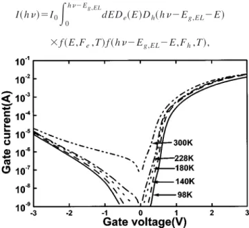
Figure 1 shows current–voltage curves of an Al/2.7 nm oxide/n-silicon PMOS diode with a circular area of 4
⫻10⫺2cm2 at different temperatures. Device temperatures
of 228, 180, 140, and 98 K are obtained from fitting of the EL line shapes, while the temperatures of the cold finger in the EL measurement are 200, 150, 100, and 10 K, respec-tively. The temperature difference is due to the device heat-ing. The EL spectra at 98 K共the cold finger at 10 K兲 has a similar line shape to the photoluminescence 共PL兲 spectra at 100 K at a pump power of 35 W/cm2共Fig. 2兲. Note that the sample temperature of the PL measurement should be close to that of the cold finger at this pump power.6The emission spectra from 300 K down to 98 K are shown in Fig. 3 with a fixed gate bias of positive 3 V and a drive current density of
⬃0.4 A/cm2
. To ensure no degradation of the device due to current stress of the ultrathin oxide, the current–voltage curves were measured before and after the EL measure-ments. Little change of the current–voltage curves was ob-served for such low drive current density. The electrolumi-nescence spectra at all measurement temperatures can be fit by the line shapes of the EHP recombination using the fol-lowing expression:
I共h兲⫽I0
冕
0h⫺Eg,EL
dEDe共E兲Dh共h⫺Eg,EL⫺E兲 ⫻ f共E,Fe,T兲f 共h⫺Eg,EL⫺E,Fh,T兲,
a兲Electronic mail: [email protected]
b兲Also with the Institute of Electro-Optical Engineering, National Taiwan
University, Taipai, Taiwan.
FIG. 1. Current–voltage characteristics at different temperature for the MOS LED.
APPLIED PHYSICS LETTERS VOLUME 77, NUMBER 8 21 AUGUST 2000
1111
where Deand Dh are the densities of states of electrons and
holes, respectively, Feand Fhare the respective quasi-Fermi
energies, h is the energy of photon emitted, T is the mea-surement temperature, Eg,EL is the band gap of Si obtained by the EL measurements, and f ’s are the Fermi–Dirac dis-tribution. Note that only the conservation of energy is taken into account in this expression, assuming that momentum conservation is achieved by Si/oxide roughness, localized holes, phonons, and other possible mechanisms.4The three-dimensional共3D兲 density of states 关D(E)⬃E1/2兴 is used for holes, while a constant two-dimensional 共2D兲 density of states is used for electrons in the accumulation layer. Table I lists the fitting parameters共temperature, electron quasi-Fermi energy, hole quasi-Fermi energy, and band gap兲 of EL spec-tra at different temperatures as well as the hole density in the oxide/Si interface estimated from the Fermi energy. Note that the electron density in the accumulation layer is two-dimensional, and the effective 共3D兲 density 共2D density di-vided by accumulation layer thickness兲 should be similar to the hole density due to charge neutrality. The theoretical line shape is a convolution between the electron population and the hole population, distinct from the free-exciton line shape
关⬃E1/2exp(⫺E/kT), where E is the photon energy and k is
the Boltzmann constant兴.7According to the Mott transition, excitons are formed at a low carrier density, while at a high carrier density, excitons dissociate into electron–hole plasma. The transition density is given by kT/16Exax
3
,7 where Exis the Rydberg exciton, and axis the Bohr exciton
radius. At 98 K, the transition density is ⬃1⫻1017cm⫺3,
while the carrier density estimated from the quasi-Fermi hole energy at 98 K in Table I is⬃2⫻1018cm⫺3. Therefore, free excitons cannot be observed at 98 K, while the thermal en-ergy共8.5 meV兲 is still lower than the exciton binding energy
共14.7 meV兲. The normalized emission intensity 共the ratio of
the integral intensity to the drive current兲 has weak tempera-ture dependence and slightly increases at low temperatempera-ture
共Fig. 4兲. The activation energy obtained from the Arrhenius
plot is 12 meV. As a comparison, the previous PL results6 showed that a large activation energy 共150 meV–280 meV兲 of PL intensity in Si/SiGe/Si quantum wells was observed, corresponding to the band-gap difference between Si and SiGe. The hole concentration in the SiGe well drops at high temperature, and this yields a lower recombination rate in the SiGe well. However, in the MOS LED, the electron concen-tration in the accumulation region of the n-type Si is mainly determined by the positive gate voltage, which is indepen-dent of temperature. This yields, relatively weak temperature dependence of EL integral intensity in the MOS LED.
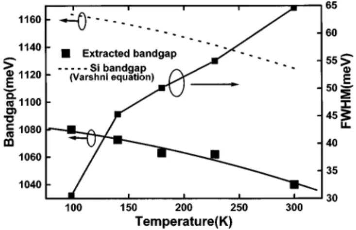
The extracted band gaps from EL spectra are⬃80 meV lower than the Si band gap obtained from the Varshni equation8at all temperatures共Fig. 5兲. The transverse optical
共TO兲 phonons as well as the longitudinal optical 共LO兲
phonons are probably involved in the light-emission process. This phonon participation is confirmed by the resemblance between the EL spectrum at 98 K and the PL spectrum at 100 K共Fig. 2兲, since it is well known that the Si PL peak is due to phonon replicas. In PL spectra at very low tempera-ture 共2 K兲, both TO 共58 meV兲 and LO 共56 meV兲 phonon replicas were observed, but the TO emission intensity is about three times that of the LO emission. For EL and PL
FIG. 4. Arrhenius plot for the normalized integral intensity of the MOS LED biased at 3 V.
TABLE I. Fitting parameters obtained from EL spectra as well as the hole density.
T共K兲 Fn共eV兲 Fp共eV兲 Eg,EL共eV兲
Hole concentration 共cm⫺3兲 300 ⫺0.088 ⫺0.07 1.04 6⫻1017 228 ⫺0.058 ⫺0.049 1.062 5⫻1017 180 ⫺0.025 ⫺0.011 1.06 2⫻1018 140 ⫺0.010 ⫺0.008 1.073 1⫻1018 98 0.005 0.005 1.08 2⫻1018
FIG. 2. Comparison between the EL spectrum at 98 K and the PL spectrum at 100 K.
FIG. 3. EL spectra of the MOS LED at different temperatures.
spectra measured at 77 K or higher, these two close lines
共only 2 meV apart兲 are not resolved, and one effective line
shape can fit the experimental data reasonably well in the SiGe PL,7as well as in the Si EL of this work. The rest of the band-gap lowering 共⬃20 meV兲 may be due to the surface bending4 and/or the band-gap narrowing at high carrier density.9 The peak widths 共full width at half maximum兲 of the EL spectra decreases from 65 to 30 meV for the tempera-ture from room temperatempera-ture to 98 K 共Fig. 5兲. This is due to the carrier filling close to the conduction-band and valence-band edges at low temperature as a result of the Fermi–Dirac distribution.
We also measured the external quantum efficiency of the MOS LED using Al as the gate electrode as well as the back contact. The external quantum efficiency is about 10⫺6 at room temperature, measuring from the edges of the Al
elec-trode. Although the Auger recombination can degrade the carrier lifetime, the external quantum efficiency does not drop up to the injection current of 100 mA. A previous simu-lation study on SiGe PL shows that the Auger recombination seems important at low temperature, not at room temperature10at the pump power of 30 W/cm2.
In conclusion, the emission intensity of the MOS LED has weak temperature dependence from room temperature down to 98 K, and increases slightly at low temperature. The emission peak is due to TO phonons as well as LO phonons. The emission process at all temperatures can be fit by the EHP model. A relatively intense EL from the MOS LED is observed, as compared to the PL.
This work is supported by the National Science Council, Taiwan, ROC共2218-E-002-017, 2218-E-002-012, 89-2112-M-002-034, and 89-2215-E-002-016兲. Support by the Tjing Ling Foundation is highly appreciated.
1Y. Q. Wang, T. P. Zhao, J. Liu, and G. G. Qin, Appl. Phys. Lett. 74, 3815 共1999兲.
2
J. Yuan and D. Haneman, J. Appl. Phys. 86, 2358共1999兲.
3C. W. Liu, M. H. Lee, C. F. Lin, I. C. Lin, W. T. Liu, and H. H. Lin, Tech.
Dig. Int. Electron Devices Meet. 749共1999兲.
4C. W. Liu, M. H. Lee, M.-J. Chen, I. C. Lin, and C.-F. Lin, Appl. Phys.
Lett. 76, 1516共2000兲.
5
A. St. Amour and J. C. Sturm, Tech. Dig. Int. Electron Devices Meet. 769
共1995兲.
6J. C. Sturm, A. St. Amour, Q. Mi, Lori C. Lenchyshyn, and M. L. W.
Thewalt, Jpn. J. Appl. Phys., Part 1 33, 2329共1994兲.
7
X. Xiao, C. W. Liu, J. C. Sturm, L. C. Lenchyshyn, and M. L. Thewalt, Appl. Phys. Lett. 60, 1720共1992兲.
8S. M. Sze, Physics of Semiconductor Devices, 2nd ed.共Wiley, New York,
1981兲, p. 15.
9
Y. Taur and T. H. Ning, Fundamentals of Modern VLSI Devices 共Cam-bridge University Press, New York, 1998兲, p. 300.
10A. St. Amour, Ph.D. thesis, Princeton University共1996兲. FIG. 5. Extracted band gap and linewidth at different temperatures. Si
band-gap data are obtained from the Varshni equation of Ref. 8.
1113