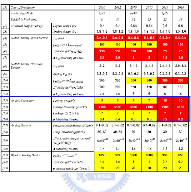
國 立 交 通 大 學
電子工程學系 電子研究所
博 士 論 文
高介電係數介電質材料應用於金氧金電容之研究
The Investigation of Metal-Insulator-Metal Capacitor
Applying High-κ Dielectrics Material
研 究 生:黃靖謙
指導教授:荊鳳德 教授
高介電係數介電質材料應用於金氧金電容之研究
The Investigation of Metal-Insulator-Metal Capacitor Applying
High-κ Dielectrics Material
研 究 生:黃靖謙
Student:Ching-Chien Huang
指導教授:荊鳳德 博士
Advisor:Dr. Albert Chin
國 立 交 通 大 學
電子工程學系 電子研究所
博 士 論 文
A Dissertation
Submitted to Department of Electronics Engineering & Institute of Electronics College of Electrical and Computer Engineering
National Chiao Tung University in partial Fulfillment of the Requirements
for the Degree of Doctor of Philosophy
in
Electronics Engineering June 2009
Hsinchu, Taiwan, Republic of China
i
高介電係數介電質材料應用於金氧金電容之研究
研究生:黃靖謙 指導教授 : 荊鳳德教授
國立交通大學
電子工程學系暨電子研究所
摘要
根據國際半導體技術藍圖制定會(ITRS),元件尺寸必須不斷的縮微,為了配 合現今類比、射頻通訊和記憶體元件的發展,金氧金電容(MIM Capacitor)的研發 是刻不容緩的。在各種不同的被動元件中,金氧金電容經常被廣泛的應用在射頻 電路裡的阻抗匹配與直流濾波器中;然而,它們通常卻占據了很大的電路面積。 此外,金氧金電容也是發展高密度動態記憶體中所面臨的重要挑戰之一。因此, 為了有效降低晶片的面積與節省成本,提高單位面積的電容值是極為需要的。為 了達到未來記憶體元件的高電容密度要求,高介電係數介電質材料的開發似乎是 唯一的選擇。當使用高介電質材料時,在增加材料的介電常數和減少元件厚度所 伴隨而來的高漏電,更是目前主要的研究議題之一。 目前高介電材料應用於金氧金電容從氮氧化矽(κ~4-7)、氧化鋁(κ~10)、氧化 鉿(κ~22)、氧化鉭(κ~25),一直發展到氧化鈮(κ~40)。但是目前在這些材料中還 無法同時達到在高電容密度下金氧金電容所需要的特性,例如:低漏電、低電壓 和低電容變化係數。因此,我們發展出新的製程和高介電係數的材料來改進金氧 金電容,例如氧化鎳(κ~30-40)、氧化鐠(κ~26-32)和鈦酸鍶(κ>50)。為了進一步改ii 善介電質低能隙的缺點,我們利用較高功函數金屬鉑或銥當作上電極,可以得到 較佳的元件特性。 雖 然 , 鈦 酸 鍶 具 有 高 介 電 係 數 , 但 較 低 的 導 帶 不 連 續 (conduction band discontinuity)和能帶寬度(bandgap),會造成較大的電流。鈦酸鍶必須要形成結晶 相才能具有較高的介電係數(κ~150-170),而要形成奈米結晶(nano-crystal)的鈦酸 鍶,則需要較高的製程溫度(>450oC),這不適用於後段製程。此外,鈦酸鍶具有 電壓電容係數(Voltage coefficient of capacitance)較高的缺點。因此,我們利用氧 化鉭具有降低漏電流以及改善電壓電容係數的特性,將氧化鉭以一定比例摻入鈦 酸鍶中,可有效降低整體元件的漏電流和電壓電容係數。此外,我們也成功發展 出一種電漿處理(Plasma treatment)介電質的方法,不但在漏電流上有明顯的改 善,也同時改良了電壓電容係數和溫度電容係數(Temperature coefficient of capacitance)。 除了基本的漏電流與低頻量測以外,我們也量測了射頻電容的高頻散射參 數。並利用模擬軟體,淬取出元件在不同頻率所具有的電容大小。除此,我們還 深入探討電容的傳導機制與電容變化跟電壓和溫度相關的成因,相信本篇論文對 未來發展高效能金氧金電容會有很大的助益。
The Investigation of Metal-Insulator-Metal Capacitor Applying
High-
κ Dielectrics Material
Student: Ching-Chien Haung Advisor: Dr. Albert Chin
Department of Electronics Engineering
& Institute of Electronics
National Chiao Tung University
Abstract
According to International Technology Roadmap for Semiconductor (ITRS), continuous increasing the capacitance density (ε κ0 / tκ) is required to scale down the device size and the cost of Metal-Insulator-Metal (MIM) capacitors which are widely for Analog, RF and DRAM functions. However, they often occupy a large fraction of circuit area. To meet these requirements, high dielectric constant (κ) materials provide the only solution since decreasing the dielectric thickness ( ) degrades both the leakage current and performance. To achieve this goal, the only choice is to increase the κ value of the dielectrics, which have evolved from SiON (κ~4-7), Al2O3 (κ=10), HfO2 (κ~22), Ta2O5 (κ~25) to Nb2O5 (κ~40).
tκ
/
C C
Δ
To further achieve the properties of MIM such as low leakage current, low voltage coefficient of capacitance and low temperature coefficient of capacitance. Thus, we have developed novel process and high-κ dielectric materials, such as TiNiO (κ~30-40), TiPO (κ~26-32) and SrTiO3 (κ>50) to achieve this technology. To
further improve the small bandgap (EG) of these dielectrics, we apply the higher
iii
work-function (φB) Pt (5.7 eV) and Ir (5.3 eV) top electrode are used to give better device performance.
Although SrTiO3 has large dielectric (κ~50-200), the small conduction band
offset ( ) and bandgap leading to larger leakage current is a larger drawback. Besides, SrTiO3 shows its higher κ values by forming nano-crystals, which is only
practicable at a higher process temperature > 450oC. Furthermore, the high voltage
coefficient of capacitance of SrTiO3 is also an important issue. Because Ta2O5 has
very low voltage coefficient of capacitance and can considerably suppressed the leakage current, the overall electrical characteristics of MIM device could be improved by doping Ta2O5 into SrTiO3 MIM capacitor. Otherwise, we have
developed a plasma treatment on dielectric to repair the defect of the dielectric to improve leakage current, voltage coefficient of capacitance and temperature coefficient of capacitance at the same time. Therefore, not only high capacitance and low leakage current, but also small voltage/temperature dependence of capacitance are obtained under limited thermal budget for back-end-integration.
Ec
Δ
In addition to the measurement of capacitance at low frequency and the leakage current, the measurement of the S-parameters to investigated the characteristics of the MIM capacitors at RF regime are also demonstrated. By using the simulation software, the capacitance density of MIM capacitors at different frequencies was extracted.
iv
v
Besides, the related factors such as understandings of the mechanism of conductivity, the voltage/temperature dependence of capacitances, barrier height, and interfacial layer were investigated, and these are also useful in the development of advanced MIM capacitors.
vi
Acknowledgement
That I exist is a perpetual surprise which is life.
- Rabindranath Tagore 我的博士求學過程-現在回想起來感覺像是一場冒險旅程。旅程 中充滿各種的關卡。每個關卡都需要一把鑰匙,而通過之後是絕無僅 有的寶物與更多的抉擇。冒險中的鑰匙是我的老師、朋友、以及家人、 甚至一些從未見過的朋友。寶物是我從錯誤中學習的人生經驗。而抉 擇是我充滿未知的人生。 在此,我想感謝我的指導教授荊鳳德老師。在過去近五年中,荊 老師扮演著亦師亦友的角色。荊老師幫助我的不僅是學業,更多的是 在我碰到難關時給我極大的幫助。從老師身上看到的是學者與家庭的 典範。荊老師不僅在研究上提供我很好的舞台,也讓我在國內的學習 環境多了國際視野與各種難得的經驗。 我第一個要感謝淳護學長。淳護學長平時花了極大的心力與我一 起討論研究方法以及協助我不少實驗上遇到的問題,淳護學長很像是 我博士班旅途中一起度過難關的好夥伴,也謝謝淳護學長的傾囊相 授。另外,要感謝的是國誠學長。是國誠學長帶領我踏入High-κ MIM 的領域,國誠學長教我很多實驗方法以及各種理論分析。我也必須要 感謝ED633實驗室的所有同學和學弟們,士豪、迺超、坤億、維邦、 思麟;謝謝他們這段期間對我的幫忙。我也必須要感謝我的高中同學 李克濤博士,謝謝克濤實驗上的協助以及生活上的幫忙。也要感謝大 學同學呂哲慶博士,感謝他在RF上給我一些指導與意見。最後我要 感謝我的父母, 黃明賜先生與陳麗雲女士,謝謝他們一路上的栽培與 伴我成長。最後要謝謝泰琳,謝謝她這些年來的相扶相持、不離不棄!
vii
Contents
Abstract (in Chinese)……….……….……….………i
Abstract (in English) ………..……….……….………….…iii
Acknowledgement……….……….……….………vi
Contents……….……….……….……...vii
Figure Captions……….……….……….……ix
Table Captions……….……….……….……xiv
Chapter 1
Introduction1.1
Motivation to study High-κ Dielectric Materials………11.2
Motivation to study MIM capacitors using high-κ dielectrics………....41.3
The Background of Metal Electrodes……….……….91.4
The Deposition method of High-κ Dielectrics……...………….………..111.5
The Evaluation of high-κ value………...………….……...…………..131.6
The measurement of the Devices………...………….……….…..131.7
Innovation and Contribution………...………….…………...………...14Chapter 2
Leakage Current Improvement of Ni/TiNiO/TaN Metal-Insulator-Metal Capacitors using Optimized N+ Plasma Treatment and Oxygen Annealing2.1
Motivation...……….………..……222.2
Experimental……….………...………..232.3
Results and discussion……….……….…….………24A. The effect of O2 PDA temperature………..………. 24
B. N+ plasma effect...26
C. Performance comparison...27
viii
Chapter 3
High Performance Ir/TiPrO/TaN MIM Capacitors for Analog ICs Application3.1
Motivation..………..…….………343.2
Experimental………..………...………….363.3
Results and discussion…………..……….…………373.4
Conclusion………..……….…..……42Chapter 4
Impact of Ta2O5 doping on Electrical Characteristics of SrTiO3 Metal-Insulator-Metal Capacitors4.1
Motivation…………...………..………..…..…544.2
Experimental………….………..………..….574.3
Results and discussion………..………...………..………584.4
Conclusion………...………..…62Chapter 5
RF TaN/SrTiO3/TaN MIM Capacitors with 35 fF/μm2 Capacitance Density5.1
Introduction………..………...………..……745.2
Experimental……….…………..………..……….755.3
De-embedding Theory....….…….…………..………..……….765.4
Results and discussion………..……….…79A. C-V and I-V characteristics…..………. 79
B. High frequencies characteristics……….………. 80
5.5
Conclusion………...………..…82Chapter 6
Conclusion and Recommendation……….………...90References……….………..…94
Vita………..………..………….…106
ix
Figure Captions
Chapter 1 Introduction
Fig. 1-1 The International Technology Roadmap of analog and mixed-signal
capacitors
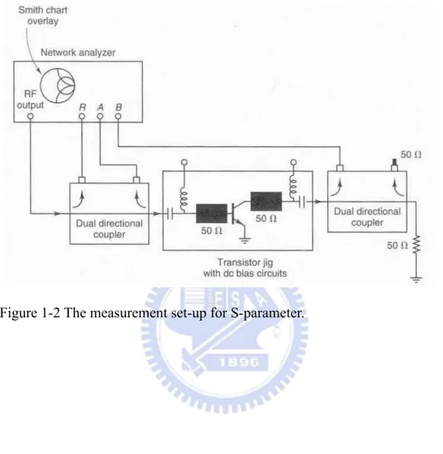
………...………19Fig. 1-2 The measurement set-up for S-parameter
………….………...20Fig. 1-3 The illustration of HP85122A and ATN-NP5B noise measurement
system
………...………...………21Chapter 2 Leakage Current Improvement of Ni/TiNiO/TaN
Metal-Insulator-Metal Capacitors using Optimized N
+Plasma Treatment and Oxygen Annealing
Fig. 2-1 (a) C-V and (b) J-V characteristics of Ni/TiNiO/TaN MIM
capacitors processed at respective 420 and 460°C O
2PDA
.……29Fig. 2-2 ΔC(V)/C-V and (b) TCC of Ni/TiNiO/TaN capacitors annealed at
420 and 460°C O
2PDA
………...………..30Fig. 2-3 (a) J-V characteristics and (b) summarized C-V and J-V data of
460°C-PDA Ni/TiNiO/TaN MIM capacitors processed under
different N
+plasma treatment
………...………...31Fig. 2-4 (a) ΔC(V)/C-V, (b) TCC, and (c) summarized
α
, TCC, and CET
of Ni/TiNiO/TaN capacitors under different N
+plasma treatment
x
and 460°C O
2PDA
………...………..33Chapter 3 High Performance Ir/TiPrO/TaN MIM Capacitors for
Analog ICs Application
Fig. 3-1 C-V characteristics of Ir/TiPrO/TaN capacitors with different
annealing temperature
measured at 1 MHz
………..45Fig. 3-2 J-V characteristics of Ir/TiPrO/TaN capacitors with different
capacitance density (16 fF/μm
2and 20 fF/μm
2) measured at (a)
25
oC and (b) 125
oC, respectively
……….46Fig. 3-3 J-V characteristics of Ir/TiPrO/TaN capacitors for capacitance
density with (a) 16 fF/μm
2and (b) 20 fF/μm
2measured from 25
o
C
to 125
oC, respectively
……….47Fig. 3-4 The comparisons of J-V for different high-κ material capacitors,
at comparable capacitance density. The leakage current of TiPrO
MIM is significantly lower than TiO
2and previous work TiTaO
and TiNiO MIM
………..……….48Fig. 3-5 Plot of ln(J) versus E
1/2under electron injection from top
electrode for Ir/TiPrO/TaN capacitors with capacitance density of
16 fF/μm
2and capacitance density of 20 fF/μm
2is shown in the
xi
the FP emission fitting at high electric field are measured at 25
oC
and 125
oC, respectively
………..………..……….49Fig. 3-6 The FP conduction fitting at high field for (a) Ir/TiPrO/TaN
capacitor and (b) Ir/TiPrO/TaN capacitor are shown. The leakage
current measured at 125
oC for Ir/TiPrO/TaN and Ir/TiNiO/TaN
MIM are also shown in (c)
………....51Fig. 3-7 The SE emission fitting of Ir/TiPrO/TaN capacitors at low electric
field
…………..………52Fig. 3-8 (a)
Δ
C/C -V characteristics of Ir/TiPrO/TaN capacitors for
different ca pacitance density. (b)The temperature-dependent
normalized capacitance for Ir/TiPrO/TaN capacitors for different
capacitance density
…………..………..………...53Chapter 4 Impact of Ta
2O
5doping on Electrical Characteristics of
SrTiO
3Metal-Insulator-Metal Capacitors
Fig. 4-1 C-V characteristics of pure STO and STO doped Ta
2O
5devices,
measured at 1MHz
………64Fig. 4-2 Free carrier injection model
………65Fig. 4-3 (a) Capacitance density at zero bias (0V) and corresponding
dielectric constant. (b) tan
δ
at 0.01 - 1 MHz frequency range for
xii
pure STO and STO doped Ta
2O
5devices
………66Fig. 4-4 J-V characteristics for pure STO and STO doped Ta
2O
5devices
measured at 25
oC
………...67Fig. 4-5
Δ
C/C -V characteristics of pure STO and STO doped Ta
2O
5devices.
………...68
Fig. 4-6 TCC characteristics of pure STO and STO doped Ta
2O
5devices
...69
Fig. 4-7 (a) C-V and (b) ΔC/C-V characteristics after CVS at 25
oC for pure
STO MIM capacitor, respectively
...70Fig. 4-8 (a) C-V and (b) ΔC/C-V characteristics after CVS at 25
oC for STO
doped Ta
2O
5MIM capacitor, respectively
...71Fig. 4-9 TCC characteristic of (a) pure STO and (b) STO doped Ta
2O
5MIM
capacitors, respectively
...72Fig. 4-10 A comparison on the extrapolated operation voltage of 10-years
life time for STO and STO doped Ta
2O
5MIM capacitor
...73Chapter 5 RF TaN/SrTiO
3/TaN MIM Capacitors with 35 fF/
μm
2Capacitance Density
Fig. 5-1 The C-V characteristics of TaN/STO/TaN MIM capacitors. Very
high capacitance density of 35 fF/μm
2is measured at 1 MHz with
xiii
small capacitance variation. The C-V results from 100 kHz to 1
MHz are measured from LCR meter and the data from 0.2 GHz to
10 GHz are obtained from the S-parameters
...84Fig. 5-2 The measured J-V characteristics of TaN/STO/TaN MIM capacitors
with large 35 fF/μm
2density
...85
Fig.5-3 (a) C/C-V plot for TaN /STO/TaN MIM capacitors
(b)Temperature-dependent normalized capacitance for TaN
/STO/TaN MIM capacitors
...86Fig. 5-4 (a) The measured and simulated two-port S-parameters for STO
MIM capacitors, from 200 MHZ to 10 GHz. (b) The equivalent
circuit model for capacitor value extraction from measured
S-parameters
...87Fig. 5-5 (a) Frequency dependent capacitance density, ΔC/C and α for a STO
MIM capacitor biased at 1.5V. The data for frequency > 1 MHz
were obtained from the S-parameters. (b) The ΔC/C characteristics
of a STO MIM capacitor at RF regime
...88xiv
Table Captions
Chapter 2 Leakage Current Improvement of Ni/TiNiO/TaN
Metal-Insulator-Metal Capacitors using Optimized N
+Plasma Treatment and Oxygen Annealing
Table 2-1 Comparison of MIM capacitors with various dielectrics and
metal electrode
...28Chapter 3 High Performance Ir/TiPrO/TaN MIM Capacitors for
Analog ICs Application
Table 3-1 Comparison of important device data for MIM Ir/TiPrO/TaN
capacitor with various high-κ dielectrics and work-function
metals
...44Chapter 4 Impact of Ta
2O
5doping on Electrical Characteristics of
SrTiO
3Metal-Insulator-Metal Capacitors
Table 4-1 Comparison of important device data for MIM capacitor with
various high-κ dielectrics
...63Chapter 5 RF TaN/SrTiO
3/TaN MIM Capacitors with 35 fF/
μm
2Capacitance Density
Table 5-1 Comparison of important device data for MIM capacitor with
various high-κ dielectrics
...831
Chapter 1
Introduction
1.1
Motivation to study High-
κ Dielectric Materials
In the scaling down of CMOS, reducing the thickness of gate stack while maintaining lower leakage current plays an important role. The leakage current of devices with the same gate dielectric reduces with the scaling down of gate length and width; however, the leakage current density increases with the scaling gate dielectrics exponentially. In other word, the gate leakage current increases as the device size degreases. The larger leakage current will lead to the degrading effect of devices’ reliability and higher power consumption of the devices. Therefore, reducing the leakage current with scaling down the device size will be a crucial issue in the development of advanced electrical devices.
Because the leakage current is strongly related to the physical thickness of dielectric layer, increasing the thickness of dielectric layer can considerably suppress the leakage current of the devices. By using the dielectric material with high dielectric constant (high-κ), the physical thickness of the dielectric layer in the devices could be increased without reducing the capacitance density. High-κ dielectric material often
exhibits poorer material properties than SiO2, such as smaller bandgap, weaker bond,
and higher defect density; however, the high-k dielectrics with the same effective oxide thickness (EOT) with SiO2 still demonstrate lower leakage current than SiO2 by several
orders. This is the reason why high-κ dielectric material plays an important role in the future advanced technology.
According to the ITRS (International Technology Roadmap for Semiconductor) [1] of SIA showing in Figure 1-1, the thickness of gate oxide is required to be below 10 after 2009. In addition, the gate length and bias voltage reduce by 11% every year while maintaining the drive current of device is needed. Thus, it is inevitable to continually scale down the gate dielectric in the proceeding CMOS technology. On the other hand, the operation frequency of the device below the generation of 100 nm will be above GIGA Hz and the electrical characteristics of high-κ dielectrics at that frequency play a crucial position for the using of high-speed electrical devices. Although several high-κ dielectrics exhibit good electrical characteristics at low frequency, their performance would possibly degrade at RF regime. Therefore, it is imperative to find out the high-κ dielectric exhibiting practicable characteristics at both high and low frequency region.
Αo
In the recent, there are some high-κ dielectrics have been widely investigated and the issues and characteristics of these dielectric material have also been reported.
3
Unfortunately, high-κ dielectrics showing good performances are often accompanied by some drawbacks. Searching for the most practicable high-κ dielectrics for the use of advanced electrical device and altering the suitable device structure or process to meet the requirement of high-speed device is the most imperative mission to apply high-κ dielectrics to the next VLSI generation.
4
1.2
Motivation to study MIM capacitors using high-
κ dielectrics
For electrical devices, especially for mobile applications, it is imperative to reduce the capacitor area since the area percentage of capacitor significantly increases with the scaling down of logic parts. In RF applications, a high degree of linearity is required for capacitors to minimize harmonic generation and improve balancing. Integration of high-quality and high-density MIM capacitors is a challenge for the RF transceiver roadmap. The need to integrate new materials in a cost-effective manner to realize high-density MIM capacitors follows the guideline published in the ITRS roadmap. Potential solutions for MIM capacitors include the introduction of high-κ dielectrics now being developed for future use for gate dielectrics [2-16]. Therefore the high-κ dielectrics used in MIM capacitors have evolved from SiON (κ~4-7) [3-5], Al2O3 (κ=10)
[13], HfO2 (κ~22) [7]-[11], Ta2O5 (κ~25) [12], [15] to Nb2O5 (κ~40) [16]. Unfortunately,
the demonstration of MIM with these films is not practicable to achieve properties, such as non-dispersive, good linearity and high breakdown with low leakage concomitantly, at high unit capacitance. To achieve this goal, some novel high-κ dielectrics have been studied, which have progress from TiO2 (κ~50-80) [17], TiHfO (κ~40-50) [18], TiTaO
(κ~40-50) [19]-[21] to SrTiO3 (STO, κ~50-200) [21]-[23].
It has been studied that titanium oxide (TiO2) exhibits several better properties
5
stability while it was integrated with TiN electrode. It allows TiO2 shows the dielectric
characteristic after high temperature process for silicide formation. Moreover, the heat conduction rate of TiO2 is higher than that of SiO2. Although TiO2 has the above merits,
there are still some major drawbacks that should be overcome, such as larger leakage current than that of other dielectrics with the same effective oxide thickness, lower breakdown voltage, and interfacial oxide layer forming after post implant RTA. However, it has been reported that thickness of the interface oxide layer could be reduced by using NH3 plasma treatment [23], but the flat-band voltage shift and the
degradation of channel mobility still occurred.
SrTiO3 (STO) is a potential candidate to increase the κ value beyond a value of 45,
It has the well-known perovskite-type structure and has a para-electric phase above 105K, and high-κ value of ~300 at room temperature. This makes it an attractive candidate for DRAM [24]-[27] due to the high charge storage capacity and para-electricity (no fatigue or aging problems). To achieve the high κ value, the STO requires a heat treatment at 450~500oC under an oxygen ambient for crystallization
[24]-[26]. Therefore, it also requires a Pt or RuO2 lower electrode[25] to withstand the
high temperature oxidation, but the high cost and availability of noble metals pose concerns for mass production.
difficulties needed to overcome. In the G-bit DRAM generation, the memory cell density is too high that the dielectrics couldn’t fill the cell space, while its thickness is larger than 20 nm. This limitation of dielectric thickness makes it impossible to use the quaternary metal oxide, such as SrTiO3 or BaSrTiO3 as the dielectric layer. Due to the
difficulties of conformal CVD for these quaternary metal oxides, the high aspect ratio of trench for DRAM is an inevitable challenge to solve.
Because of the high dielectric constant, minimum thickness limit and good ability of step coverage, simple metal oxide such as Ta2O5, Al2O3, ZrO2, HfO2 and Pr2O3 are
thought as the promising dielectric materials in the development of advanced DRAM technology. Among these dielectrics, ZrO2, HfO2 and Pr2O3 exhibit larger conduction
band offset (ΔEc~0.5 eV), bandgap (~4-6 eV), dielectric constant (κ~ 15-25) and bond enthalpy to prevent from larger leakage current and obviously degradation after high temperature process. Similar to high- κ /Si CMOSFET, the larger conduction band offset is the better choice for MIM capacitor. Due to their moderate permittivity, it is difficult to meet dielectric layer with an EOT well below 1.0 nm. One solution to raise the permittivity is combining them with very high-κ dielectric, such as TiO2 with high
permittivity value of 50-80 contributing from the soft phonons. From above discussion, we know TiO2-based dielectric material combined with moderate high-κ and large
bandgap and conduction band offset materials will be a suitable approach for logic
7
devices (metal gate/high-κ) or DRAM technology beyond 45 nm.
On the other hand, in order to fabricate monolithic microwave integrated circuits successfully, it is required to meet reliable, repeatable, and predictable performance for both active and passive components. Among them, the capacitor used in filtering, decoupling and network matching plays a significant role in front end or mixed signal circuits. Therefore, capacitors with high capacitance density, low voltage coefficient, good capacitor matching, precision control of values and low parasitic effects are required. By using thin dielectric film with high dielectric constant, the capacitance density could be considerably increased. Recently, some kinds of dielectrics and methods have been reported to meet the goal of high capacitance density and good characteristics.
Moreover, it is also essential to investigate the interface between the electrode and high-κ dielectric layer, especially the bottom electrode which is being exposed to the precursors during the deposition. During the post annealing process, there will be interfacial layer form between bottom electrode and dielectric layer. There will be traps and defects in the interfacial layer. Since it is know that leakage can be interface or bulk dominated. If the thickness of interfacial layer is thicker, the leakage current would be higher due to more traps formation. In addition, it has been reported the traps present in the dielectric also resulted in the dispersive capacitor behavior. It is thus, useful and
8
9
1.3
The Background of Metal Electrodes
The Metal-Insulator-Metal (MIM) structure can reduce the contact resistance and increase the storage charge with comparison to Metal-Insulator-Semiconductor (MIS) structure. MIM capacitors are often integrated in the back end part of process flow. In the back end process, the maximum process temperature is restricted by the thermal budget.
As DRAM density increasing, devices shrinkage and higher charge storage is inevitable. It is difficult for conventional MIS structure to achieve the requirements, so MIM structure is expected to apply in the trench DRAM process. Therefore, the interaction between high-κ dielectric layer and metal electrode is not been anticipated. If high-κ material interacts with the metal electrode, there will be an interfacial layer forming between high-κ material and metal electrode. The interfacial layer will change the properties of whole dielectric film, such as interface roughness, interface stress, electron barrier height, thermal stability, etc.
The demand for advanced materials in the DRAM trench capacitor is delayed compared to the stacked capacitor by only a few years. Several high-κ materials are currently used in the Silicon-Insulator-Silicon (SIS) structure for DRAM trench capacitors, but a metal-top electrode will be needed in 2007 and a full MIM structure with high-κ material may be needed until 2009.
10
The electrodes of MIM capacitors are fabricated using metals such as TaN, TiN, etc., which are often deposited using CVD (chemical vapor deposition), ALD (atomic layer deposition) or MOCVD (metal organic chemical vapor deposition) methods. Low-temperature electrode deposition process (< 450oC) is required for MIM capacitors
11
1.4
The Deposition method of High-
κ Dielectrics
Several methods to deposit thin high-κ dielectrics have been proposed in recent years and these various methods each exhibit the merits while there are some issues needed to overcome.
Recently, atomic layer chemical vapor deposition (ALCVD) has attracted much attention due to its self-limit and mono-layer deposition properties. ALCVD is the method using MCL4 (M: Hf, Ti, Zr….) and H2O as sources to deposit high-κ dielectrics.
The precursors are introduced into the heated chamber and substrates. The reaction only occurs in the substrate surface instead of the deposited layer and each layer is deposited at a time. Therefore, the thickness of dielectrics could be controlled precisely and is dependent on the process cycle linearly. Although the excellent uniformity of deposition can be achieved on SiO2 and Si3N4, the directly deposition on H-terminated Si substrate
would lead to rough surface. Unfortunately, H-terminated Si substrate is inevitable after HF dipping. Therefore, the improvement of process precursor is the key point to overcome the issues of ALCVD deposition.
Metalorganic chemical vapor deposition (MOCVD) is the other dispositive method wildly used in VLSI fabrication. The dielectrics are deposited by using metal organic precursor vapor. During the deposition process, the precursors are introduced into low-pressure chamber and the substrate is heated to some suitable process
12
temperature. The uniform and conformal deposition of dielectrics can be obtained by using MOCVD. This is why MOCVD process is integrated into fabrication process flow extensively. Although MOCVD have many merits, it still has some issues, such as carbon contamination and the impact of precursors to the environment and health.
Using PVD method to deposit the metal or metal oxide directly on the substrate followed by thermal oxidation and annealing is the other method to deposit dielectrics. In the past five years, there are many reports about this technology. In the beginning of the deposition process, the pre-clean Si substrate is loaded into high vacuum chamber immediately to prevent from native oxide formation. Following, the metal layer is deposited using reactive dc magnetron sputtering with oxygen modulation technique. Or, the metal oxide layer is sputtering directly followed by annealing. This method could be compatible with the modern VLSI process; however, the formation of interfacial oxide and crystallization are the crucial issues required to be solved. By combining the nitridation and dielectrics doping techniques, the above problems could be minimized. Thus, this dispositive method is still practicable due to the merits.
In our studies, the PVD method is used to deposit the high-κ dielectrics layer. Before high-κ dielectric layer deposition, we utilized NH3 plasma treatment on the
bottom electrode. Then, the pre-cleaned Si wafer was loaded into E-beam evaporator under high vacuum condition. After depositing the dielectric film, it was subsequently
oxidized in O2 ambient followed by annealing. The devices using TiNiO, TiPrO, SrTiO3,
and SrTiO3 doped Ta2O5 are fabricated and measured at high and low frequencies.
1.5
The evaluation of high-
κ value
First, we consider our MIM capacitor: 0A
C t
κε
= (1.1) where κ is the dielectric constant (also referred to as the relative permittivity in this article) of the material, ε0is the permittivity of free space (8.85×10⁻³ fF/μm), A is the area of the capacitor, and t is the thickness of the dielectric. This expression for C can be rewritten in terms of teq and κox (=3.9, dielectric constant of SiO2) of the capacitor. The
term teq represents the theoretical thickness of SiO2 that would be required to achieve the
same capacitance density as the dielectric: 3 0 2 3.9 3.9 8.85 10 (fA/μm) 3.9 8.85 (unit : ) (fA/μm ) eq
high k high k high k
t n C C C ε − − − − × × × × = = = m (1.2)
Thus, the high-κ value of an alternative dielectric employed to achieve the equivalent capacitance density of teq can be obtained from the expression:
3.9 high k high k eq t t κ − − × = (1.3)
1.6
The measurement of the Devices
To investigate the electrical characteristics of our devices, we measured the leakage current using HP 4156A semiconductor parameter analyzer. Besides, HP4284A
14
precision LCR meter was used to evaluate the capacitance density and the conductance ranging from 100 kHz to 1 MHz. Furthermore, to investigate the characteristics of our devices at the frequency above 1 MHz, we measured the scattering parameter using HP8510C network analyzer and the test set. The measurement set-up for S-parameter is shown in Figure 1-2. Network analyzer generates a calibrated RF signal and has three input measuring channels. These are commonly called the R, the A, and the B channels. The R channel is used to measure the incident voltage, and the A and B channels measure reflected and transmitted voltages. Then, we can obtain S11 and S21 by
calculating A/R and B/R in polar form, respectively. The S12 and S22 can also be
obtained using the same way except changing the input voltage channel. The noise figure and associated gain were measured by HP85122A and ATN-NP5B noise parameter extraction system (shown in Figure 1-3) up to 6 GHz. There are three major categories of measurement type that the system can supply: DC, S-parameters, and noise parameters. The first two categories mainly support the noise parameter measurement.
1.7
Innovation and Contribution
The overall objective of this thesis is to achieve a fundamental understanding of the working principles and the implementation issues of the Metal-Insulator-Metal capacitor and to demonstrate the novel high-κ dielectric material, electrode gate and treatment approaches for our device. The innovation of this thesis and the major topics it
15
addresses are as follows.
First, we have investigated the effects of N+ plasma treatment and oxygen
annealing on Ni/TiNiO/TaN capacitors. The novel high-κ TiNiO dielectric material is first studied in this work and the Ni top electrode is used instead of the other high work function metal electrode, such as Pt or Ir. The post deposition annealing of TiNiO under oxygen ambient increases the capacitance density but trades off the increased leakage current. This leakage current could be considerably reduced by applying an optimized N+ plasma treatment on the dielectric film. At high capacitance density of 17.1 fF/μm2, a
low leakage current of 7.7× 10⁻⁶ A/cm2 at 1 V is obtained.
Second, we demonstrate high quality material TiPrO and high density TixPr1-xO
(x~0.67) metal-insulator-metal (MIM) capacitors using high work function (~5.3 eV) Ir top electrode. Pr2O3 is one of attractive rare earth metal oxides with many merits such
as large conduction band offset (ΔEC~ 1 eV), moderate dielectric constant (κ~15) and large bandgap (EG ~4 eV). Furthermore, significantly large Gibbs free energy of Pr2O3
(+106 kcal/mol) in contact with silicon can avoid metal/oxide inter-diffusion or chemical reaction caused by oxygen exchange, which not only reduce the interfacial layer between dielectric layer and bottom electrode but also performs excellent thermal stability. Combining above advantages of high-κ Pr2O3 with the high dielectric
without scarifying capacitance density. Very low leakage current of 7×10⁻⁹ A/cm2 at -1
V and high 16 fF/μm2 capacitance density are achieved for 400 oC anneal TiPrO, which
also meets the ITRS goals (at year 2018) of 10 fF/μm2 density and
. Furthermore, the improved high 20 fF/μm2 capacitance
density TiPrO MIM is obtained at higher annealing temperature, wherelow leakage current 1.2×10⁻⁷ A/cm2 is measured at -1 V. These good performances indicate TiPrO
MIM is suitable for analog/RF ICs Applications. /( ) 7 fA/(pF )
J C V⋅ < ⋅V
Third, the impact of Ta2O5 doping on electrical characteristics of SrTiO3 MIM
capacitors was studied for the first time. Using high-κ Ta2O5 doped STO dielectric (PDA
temperature:420oC)
, an absolute value of quadratic voltage coefficient of capacitance
(VCC-α ) of 420 ppm/V2 and high capacitance density of ~20 fF/μm2 are achieved in
this work. This is approximately one order of magnitude better than the same device using a pure STO, with added advantages of improved voltage and temperature coefficients of capacitance. Besides, the degradation of electrical properties (the capacitance variation versus voltage, VCC-α, and the long-term reliability) after stress are all reduced, in contrast with using a pure STO. Therefore, this doping method has merit for achieving both low VCC and maintaining high capacitance density beyond previous STO MIM studies. Moreover, although nano-crystallized STO shows higher κ values and good device characteristics, the nano-crystallized STO requires a heat
17
treatment at 450~500oC under an oxygen ambient. This activation maximum
temperature (>450oC) cannot permit for the backend integration. In this study, the
improvement on VCC by using amorphous Ta2O5 doped STO MIM capacitors with low
thermal budget (420oC) could be achieved.
Finally, in this thesis, we achieved high-κ value to 169 and capacitance density to 35 fF/μm2, or capacitance-equivalent-thickness (CET) of 0.99 nm for unified
multi-functional SoC. Such large capacitance density with low leakage current was achieved by using very high-κ SrTiO3 (STO) with formed nano-crystals (4.3 nm). This
small poly grain size is also important to reduce variation among devices. In addition, a plasma nitridation was applied to bottom TaN that prevents CET degradation by forming interfacial TaON during STO post-deposition anneal (PDA) or using expensive conductive noble electrodes, such as Pt, Ru, and Ir. Moreover, we have studied STO MIM capacitor for RF application. Very high capacitance density of 35 fF/μm2, high κ value of 169 and small capacitance variation with frequency and
voltage are obtained at the same time that demonstrates the excellent device performance for RF application. These high performance capacitors can drastically reduce the RF capacitor area, yet can be fabricated with full compatibility with current VLSI process lines. Although this work could achieve high capacitance density and low leakage current at the same time, but its higher PDA temperature (>450oC) to form
18
Figure 1-1 The International Technology Roadmap of analog and
mixed-signal capacitors.
Figure 1-2 The measurement set-up for S-parameter.
Figure 1-3 The illustration of HP85122A and ATN-NP5B noise
measurement system.
Chapter 2
Leakage Current Improvement of
Ni/TiNiO/TaN Metal-Insulator-Metal
Capacitors using Optimized N
+Plasma
Treatment and Oxygen Annealing
22
≤
2.1 Motivation
Metal-insulator-metal (MIM) capacitors are widely used in integrated circuits (ICs) for analog, radio frequency and dynamic random access memory applications. The performance requirements of MIM capacitors are the high capacitance density, low leakage current, small voltage dependence of the capacitance (ΔC/C) and low process temperature 400°C for back-end integration. To meet these goals, both high-κ dielectric TiNiO and high work function electrode Ni are demonstrated. It is important to note that TiNiO is the low cost dielectric deposited by plasma vapor deposition (PVD) rather than the absolute high cost needed for atomic layer deposition which is usually used for some recent works like ZrO2 with distinct low-κ value comparing to our TiNiO
case.
The TiNiO is another potential dielectric material with a value of 30 –40 that was obtained under an O2 postdeposition annealing (PDA) at 420–460°C. However, it
23
also requires a Pt or RuO2 bottom electrode [25] to withstand such high temperature
oxidation, but the high cost noble metals pose concerns for mass production. To address this issue in this paper we have fabricated TiNiO MIM capacitors on conventional bottom electrode TaN, where a NH3 plasma treatment on TaN has been used to improve
electrode stability, so the capacitance density degradation by forming interfacial TaOx
during PDA will obviously decrease. Besides, Binding energy between Nickel and Oxygen (855 eV~861 eV) [41] is significantly larger than the binding energy between Tantalum and Oxygen (~530 eV) [42] and Titanium and Oxygen (~457eV) [65], which causes strong binding between Nickel and Oxygen atoms. This indicates the more complete oxidation of the dielectric film which leads to its better dielectric properties than that of other dielectrics, such as TiTaO and TiO2 [66].
To improve the leakage current, additional N+ plasma treatment on TiNiO and
high work-function Ni (5.1 eV) top electrode are applied during device processing. Based on these process methods, high 17.1 fF/μm2 density and low 7.7×10⁻⁶ A/cm2
leakage current at 1 V are simultaneously measured, which shows near two orders lower leakage improvement than previous TiNiO data. Such good device integrity indicates the good potential for TiNiO dielectric and high work-function Ni electrode for MIM capacitor application..
24
2.2 Experimental
The MIM capacitors were fabricated on 4 μm SiO2 which had been deposited on a
Si wafer. The lower capacitor electrodes were formed by depositing 0.05 μm TaN on a 1 μm Ta layer, where the thick Ta was chosen to reduce the parasitic resistance of the electrode and the TaN served as a barrier layer for the TiNiO. After patterning the lower electrode, the TaN was treated by NH3 plasma nitridation at 100 W, to improve the lower
interface. Then the TixNi1-xO (x~0.65) dielectric with 19 nm was deposited by PVD
dielectric layers were then deposited using RF magnetron sputtering. This was followed by 20W and 40W N+ plasma treatment on the dielectric for 5 min and then 420oC to
460oC furnace annealing for 30 min under oxygen ambient subsequently to reduce the
leakage current. Finally, Ni was deposited and patterned to form the top capacitor electrode. The fabricated MIM capacitors were characterized by current-voltage (J-V) and capacitance-voltage (C-V) measurements using an HP4156C curve tracer and HP4284A precision LCR meter, respectively.
4.3
Results and discussion
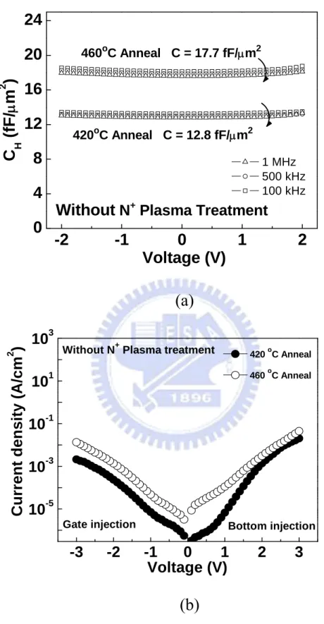
A. The effect of O2 PDA temperatureFigures 2-1(a) and 1(b) show the C-V and J-V characteristics of
Ni/Ti0.35Ni0.65O/TaN MIM capacitors under 420 and 460°C annealing, respectively.
Capacitance density increases from 12.8 to 17.7 fF/μm2 with increasing O
2 PDA
higher capacitor density, which may be due to more complete oxidation of the dielectric. From the measured capacitance density, a high-κ value of 27 was obtained for 420°C annealed TiNiO that becomes higher to 39 after increasing O2 annealing temperature to
460°C. The low leakage current of 5×10⁻⁵ A/cm2 (−1V) is measured at 17.7 fF/μm2
capacitance density using Ni electrode that is significantly better than the previous TiNiO data of > 10−4 A/cm2 (1V) at lower 14.3 fF/μm2 density with Al top electrode
[30]. Such improvement may be due to the discriminative work function between Ni (5.1 eV) and Al (4.25 eV) and higher TiO composition. In addition, the higher anneal temperature does not cause the underlying TaN film to oxidize apparently because of the improved TaN electrode stability after NH3 plasma treatment.
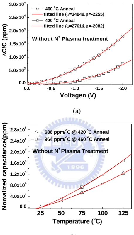
Figure 2-2(a) shows ΔC/C-V characteristics of Ni/TiNiO/TaN capacitors annealed at 420 and 460°C, respectively. The lines in the figure are fits to the data using the expression in the following expression:
6 ( ) (0) 10 (0) ppm C C V C V C C 2 V α β ⎡ ⎤ Δ − × =⎢ ⎥ = + ⎣ ⎦ (2.1) The α and β are quadratic and linear voltage coefficient of capacitance, respectively. Since β can be compensated by appropriate circuit design [31], α is the dominant factor for the undesired /C. The α for 460°C annealed TiNiO device is larger than that annealed at 420°C, which is related to the higher capacitance density and larger leakage current at higher 460°C temperature. Figure 2-2(b) shows the temperature
( ) /
C V C
Δ
26
coefficient on capacitance (TCC) obtained from normalized capacitance of Ni/TiNiO/TaN MIM capacitor at frequency of 1 MHz. Again the TCC is higher for 460°C annealed sample than that of 420°C. Thus, a trade-off the capacitance density with α and TCC is needed based on device requirement.
B. N+ plasma effect
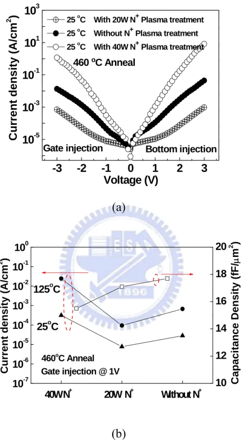
To further improve the device performance with 460°C O2 PDA, a N+ plasma
treatment on TixNi1−xO dielectric is applied. Figure 2-3(a) shows the J-V characteristics
of Ni/TiNiO/TaN capacitors processed at different N+ conditions and 460°C O
2 PDA,
where the capacitance density and leakage current are summarized in Figure 2-3(b). The capacitor with 20 W N+ plasma treatment shows significant improvement on leakage
current to 7.7 × 10⁻⁶ A/cm2 at 17.1 fF/μm2 capacitance density. This improvement of
leakage current may arise from the nitrogen atom assists to passivate oxygen vacancies in the TiNiO dielectric and eliminate the electron leakage path mediated by the oxygen vacancies [32]-[34]. However, increasing N+ plasma to 40 W, the leakage current is
even worse than the untreated one, which may be due to the plasma damage at larger energy. The higher oxidation temperature and moderate N+ plasma treatment largely
improve the device performance.
Figures 2-4(a)~4(c) show the ΔC/C-V, TCC, and summarized α, TCC, and capacitance equivalent thickness (CET) results of the Ni/TiNiO/TaN capacitors under different N+ treatment conditions. The capacitors with 20 W N+ plasma treatment not
27
only reduce the leakage current but also improve the α and TCC, which may be due to the better TiNiO dielectric property by atomic N passivation to defects.
C. Performance comparison
The important device parameters for the MIM capacitors are summarized in Table 2-1. Among the various high-κ capacitors, the Ni/TiNiO/TaN MIM capacitor, made using a high work-function Ni electrode and high-κ TiNiO dielectric, shows high capacitance density and low leakage current that are comparable with or better than the best reported data in the literature.
2.4 Conclusion
In this work, the different O2 PDA temperature, N+ plasma treatment, high work
function Ni electrode were applied to TiNiO MIM capacitors. High capacitance density of 17.1 fF/μm2 and low leakage current of 7.7 × 10⁻⁶ A/cm2 at 1 V are obtained in
Ni/TiNiO/TaN MIM capacitors. Such good capacitor device performance suggests a potential use of the Ni/TiNiO/TaN capacitor for IC applications.
28
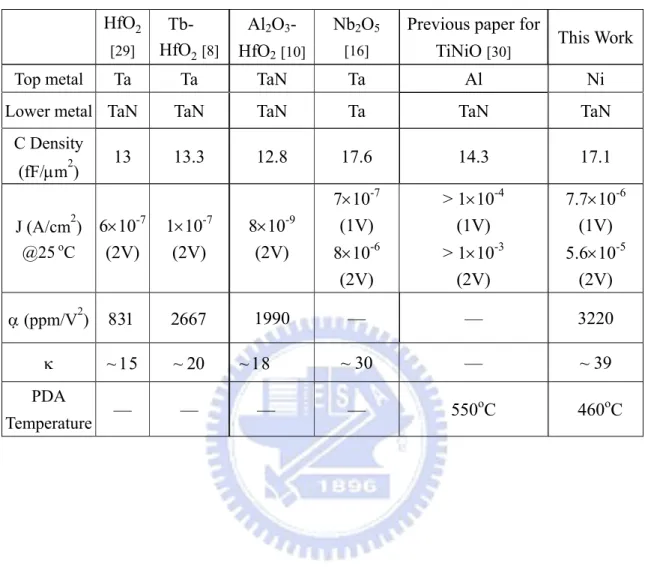
Table 2-1. Comparison of MIM capacitors with various dielectrics and metal electrode.
HfO2 [29] Tb- HfO2[8] Al2O3- HfO2[10] Nb2O5 [16]
Previous paper for
TiNiO [30] This Work
Top metal Ta Ta TaN Ta Al Ni
Lower metal TaN TaN TaN Ta TaN TaN
C Density (fF/μm2) 13 13.3 12.8 17.6 14.3 17.1 J (A/cm2) @25 oC 6×10⁻⁷ (2V) 1×10⁻⁷ (2V) 8×10⁻⁹ (2V) 7×10⁻⁷ (1V) 8×10⁻⁶ (2V) > 1×10⁻⁴ (1V) > 1×10⁻³ (2V) 7.7×10⁻⁶ (1V) 5.6×10⁻⁵ (2V) α (ppm/V2) 831 2667 1990 — — 3220 κ ~ 15 ~ 20 ~ 18 ~ 30 — ~ 39 PDA Temperature — — — — 550 oC 460oC
-2
-1
0
1
2
0
4
8
12
16
20
24
460oC Anneal C = 17.7 fF/μm2Without
N
+Plasma Treatment
420oC Anneal C = 12.8 fF/μm2 1 MHz 500 kHz 100 kHz
Voltage (V)
C
H(fF
/
μ
m
2)
(a)
-3
-2
-1
0
1
2
3
10
-510
-310
-110
110
3Without N+ Plasma treatment
Bottom injection Gate injection
Voltage (V)
Curr
ent density (A/cm
2
)
420 oC Anneal460 oC Anneal
(b)
Figure 2-1(a) C-V and (b) J-V characteristics of Ni/TiNiO/TaN MIM
capacitors processed at respective 420 and 460°C O
2PDA.
0.0 -0.5 -1.0 -1.5 -2.0 0.0 5.0x10³ 1.0x10⁴ 1.5x10⁴ 2.0x10⁴ 2.5x10⁴ 3.0x10⁴
Without N+ Plasma treatment
460 oC Anneal
fitted line (α=3404& β=-2255)
420 oC Anneal
fitted line (α=2761& β=-2082)
Δ
C/
C (p
p
m
)
Voltagen (V)
(a)
25
50
75
100
125
0.0 4.0x10⁴ 8.0x10⁴ 1.2x10⁵ 1.6x10⁵ 2.0x10⁵ 2.4x10⁵ 2.8x10⁵Without N+ Plasma Treatment 686 ppm/oC @ 420oC Anneal 964 ppm/oC @ 460 oC Anneal
Nomal
ized capaci
tance(ppm)
Temperature (
oC)
(b)
Figure 2-2
(a) ΔC(V)/C-V and (b) TCC of Ni/TiNiO/TaN capacitors annealed at 420 and 460°C O2 PDA.-3
-2
-1
0
1
2
3
10
-510
-310
-110
110
3 Bottom injection Gate injectionVoltage (V)
C
u
rre
n
t dens
ity (A
/cm
2
)
25 oC With 20W N+ Plasma treatment25 oC Without N+ Plasma treatment
25 oC With 40W N+ Plasma treatment
460 oC Anneal
(a)
10
-710
-610
-510
-410
-310
-210
-110
010
12
14
16
18
20
460oC Anneal25
oC
125
oC
Gate injection @ 1V 40W N+ 20W N+ Without N+Cap
acitan
ce Densi
ty (fF/
μm
2)
Curr
e
n
t de
ns
ity
(A
/c
m
2)
(b)
Figure 2-3 (a) J-V characteristics and (b) summarized C-V and J-V data of
460°C-PDA Ni/TiNiO/TaN MIM capacitors processed under different N
+plasma treatment.
0.0 -0.5 -1.0 -1.5 -2.0 0.0 5.0x10³ 1.0x10⁴ 1.5x10⁴ 2.0x10⁴ 2.5x10⁴ 3.0x10⁴ 3.5x10⁴ 4.0x10⁴ 460 oC Anneal
Without N+ Plasma treatment fitted line (α=3404& β=-2255)
With 20W N+ Plasma treatment fitted line (α=2933& β=-1052)
With 40W N+ Plasma treatment fitted line (α=4269& β=-3028)
Δ
C/
C (p
pm)
Voltage (V)
(a)
25
50
75
100
125
0.0 4.0x10⁴ 8.0x10⁴ 1.2x10⁵ 1.6x10⁵ 2.0x10⁵ 2.4x10⁵ 2.8x10⁵ 775 ppm/oC @ With 20W N+ Treatment 964 ppm/oC @ Without N+ Treatment 1553 ppm/oC @With 40W N+ Treatment 460oC AnnealNom
a
lized capacitance(ppm)
Temperature (
oC)
(b)
32
10
310
41
2
3
CET (nm)
VCC
α
(ppm/V
2); TCC (pp
m
/
oC)
TCC α (VCC)40W N
+20W N
+W/O N
+ CET 460 oC Anneal(c)
Figure 2-4 (a) ΔC(V)/C-V, (b) TCC, and (c) summarized α, TCC, and CET
of Ni/TiNiO/TaN capacitors under different N
+plasma treatment and 460°C
O
2PDA.
34
Chapter 3
High Performance Ir/TiPrO/TaN MIM Capacitors
for Analog ICs Application
3.1 Motivation
The technology evolution for Metal-Insulator-Metal (MIM) capacitors [5-23] requires higher capacitance density with low leakage current at evaluating temperature [1]. Besides, the MIM capacitors are also used for Analog/RF ICs and DRAM technology. Since the capacitance density equals ε0κ/tκ, the only method for higher
density, without increasing unwanted leakage current by decreasing dielectric thickness (tκ), is to use higher dielectric constant dielectric (κ) materials. One major drawback for
higher-κ MIM device is the large leakage current due to low conduction band offset (ΔEC) at evaluated temperature that leaks out the stored charge in capacitor (Q=C⋅V). However, increasing dielectric constant (κ) usually leads to decreasing of ΔEC with respect to the electrode. This is also the challenge of flash memory but unavoidable during IC operation due to large circuit density and high DC power dissipation due to leakage current. The possible solution is using high bandgap (EG) dielectric to form the
laminate [8] or multi-layer structure [10], but the overall κ value and voltage coefficient of capacitance (VCC) are largely degraded. Pr2O3 is one of attractive rare earth metal
35
oxides with many merits such as large conduction band offset (ΔEC~ 1 eV) [36], moderate dielectric constant (κ~15) and large bandgap (EG ~4 eV) [36]. Furthermore,
significantly larger Gibbs free energy of Pr2O3 (+106 kcal/mol) [37]-[39] in contact with
silicon than that of TiO2 (+7.5 kcal/mol), Ta2O5 (-52 kcal/mol), HfO2 (+47 kcal/mol) and
NiO (-51.4 kcal/mol) can avoid metal/oxide inter-diffusion or chemical reaction caused by oxygen exchange, which not only reduce the interfacial layer between dielectric layer and bottom electrode but also performs excellent thermal stability. Combining above advantages of high-κ Pr2O3 with the high dielectric constant of TiO2 (~50), mixed TiPrO
dielectric overcomes the issue of leakage current without scarifying capacitance density. In this paper, we report Ir/TiPrO/TaN capacitors with capacitance density of 16 fF/μm2 and further improved capacitance density of 20 fF/μm2 using higher annealing
temperature. High-κ values 26-32 were obtained in this work by using mixed TixPr1-xO(x~0.67). By using high-κ TiPrO with the ratio of Ti to Pr 2:1 and high work
function electrode Ir, we can achieve high capacitance density of 16-20 fF/μm2, and low
leakage current of 7×10⁻⁹ A/cm2 to 1.2×10⁻⁷ A/cm2 at 25 oC at -1 V, small quadratic VCC
(α) of 1720~2174 ppm/V2, and small TCC of 532~758 ppm/oC. The lower leakage shows improved quadratic VCC (α) and TCC, which are important for analog/RF functions. It would be important to note that the device shows large orders of magnitude lower thermal leakage at 25 oC and 125 oC at -1V than our previous work on TiTaO [19]
36
and TiNiO [35], at comparable capacitance density. Such good device integrity is due to the mixed high-κ TiPrO (κ~26-32) with larger bandgap (EG~4 eV), larger high-κ/Si
conduction band offset (ΔEC~1 eV) and larger Gibbs free energy (+106 kcal/mol) of Pr2O3.
3.2 Experimental
After depositing 2 μm SiO2 on a Si wafer, the lower capacitor electrode was
formed using PVD-deposited TaN/Ta bi-layers. The Ta was used to reduce the series resistance and the TaN served as a barrier layer between the high-κ TiPrO and the Ta electrode. The TaN was treated by NH3 plasma nitridation at 100W to improve the
bottom interface. The TaN layer with NH3 surface nitridation [22]-[23] can improve
electrode stability and prevent CET (capacitance equivalent thickness) degradation by forming interfacial TaON during post-deposition anneal (PDA). Then 14 nm thick TixPr1-xO (x~0.67) dielectric layer were deposited on the TaN/Ta electrode by PVD
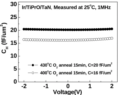
respectively followed by 400 oC and 430 oC oxidation and annealing step to reduce the
leakage current. Finally, Ir was deposited and patterned to form the top capacitor electrode. The fabricated devices were characterized by C-V and J-V measurements using an HP4155B semiconductor parameter analyzer and an HP4284A precision LCR meter.
3.3 Results and discussion
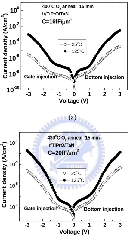
Figure 3-1 shows the C–V characteristics of Ir/TiPrO/TaN capacitors, which were processed differently. The capacitance density increased from 16 to 20 fF/μm2 with
increasing O2 PDA temperature from 400 oC to 430 oC.In Figure 3-2(a) and 3-2(b), we
perform the J–V characteristics of the TiPrO MIM capacitors with capacitance density of 16 fF/μm2 and 20 fF/μm2 respectively, measured at 25 and 125 °C. The good J-V and
C-V characteristics are obtained with the use of high work function top electrode Ir
(~5.27 eV) and nitrogen plasma (N+) treatment on bottom electrode TaN. The nitrogen
plasma (N+) treatment reduces the interfacial layer growing between the bottom
electrode TaN and TiPrO layer during oxygen annealing [22]-[23]. It is very important to note that the TiPrO MIM with capacitance density of 16 fF/μm2 achieves the ITRS goals
(at year 2018) [1] of 10 fF/μm2 density and /(J C V⋅ ) 7 fA/(pF< ⋅V). This excellent
result indicates TiPrO is a potential material candidate for future electrical device application.
To further evaluate the device performance, Figure 3-3(a) and 3-3(b) show the temperature-dependent J-V characteristics of TiPrO MIM capacitors at capacitance density of 16 and 20 fF/μm2, respectively. The leakage current increases rapidly with
increasing temperature; however, the high temperature operation is unavoidable for modern high performance IC due to the increasing power consumption. In addition, the
unwanted interfacial layer between bottom electrode and high-κ dielectric layer would lead to surface roughness between them. The interface layer make the thermal leakage current of the electron bottom injection (voltage= 0~3 V) slightly larger than the leakage of the electron gate injection (voltage= 0~-3 V), which can be observed in Figure 3-2. Thus, we only perform the J-V characteristics under reverse bias in Figure 3-3.
The examination of device performance with comparable capacitance density at 25 oC is performed in Figure 3-4. We can see the leakage current of TiPrO MIM is
significantly lower than TiO2 MIM and our previous work TiTaO MIM and TiNiO MIM,
at a comparable capacitance density. The lower leakage current of TiPrO MIM is due to the higher ΔEC between metal and high-κ TiPrO interface, higher bandgap of
high-κ TiPrO and larger Gibbs free energy of Pr2O3, which reduce the leakage current
exponentially. We also plot ln(J) versus E1/2 relation in Figure 3-5. The
temperature-dependent leakage current in MIM is typically governed by Schottky emission (SE) or Frenkel-Poole (FP) as:
⎟⎟ ⎠ ⎞ ⎜ ⎜ ⎝ ⎛ − ∝ kT V E J 2 b 1 exp γ (3-1) 1 2 3 0 q K γ ηπε ∞ ⎛ ⎞ = ⎜ ⎝ ⎠⎟ (3-2) The η is equal to 1 or 4 for FP or SE case and K∞ is the high-frequency
dielectric constant (=n2). The refractive index n =2.3 for Ti
xPr1-xO (x~0.67) is reasonable
39
by linear interpolation of the reported 2.57 for TiO2 and 1.75 for Pr2O3. From Figure 3-5,
the leakage at 25 oC from Ir top electrode on TiPrO/TaN is ruled by SE at low field and
FP at high field by trap-conduction. Besides, the leakage at 125 oC is also dominated by
SE at low field and FP at high field. This result would be due to the large ΔEC of TiPrO and the larger energy barrier φb of Ir electrode. The different slopes γ , for the SE and FP
cases arise from the different energy barriers φb, corresponding tothe work function of
the metal-electrode/dielectric in the SE case or the trap energy level in the dielectric for the FP case.
Since the conduction mechanism at high electric field for Ir electrode on TiPrO is governed by Frenkel-Poole Emission, we plotted the ln(J/E)-1/KT relation of TiPrO in Figure 3-6(a) to extract the trapping level. The larger Gibbs free energy of Pr2O3 (+106
kcal/mol) contacted with silicon avoids metal/oxide inter-diffusion. Above reason indicates the interfacial trap density of TiPrO (between dielectric and electrode) would be smaller than that of other dielectrics, such as TiTaO and TiNiO. Thus, the trapping energy in the TiPrO dielectric will be larger than TiTaO (~0.3 eV) [19] and TiNiO [35]. Besides, the binding energy between Praseodymium and Oxygen (928 eV~970 eV) [40] is significantly larger than the binding energy between Nickel and Oxygen (855 eV~861 eV) [41] and that between Tantalum and Oxygen (~530 eV) [42], which causes stronger binding between Praseodymium and Oxygen atoms [66]. This indicates the more
complete oxidation of the dielectric film which leads to its better dielectric properties than that of other dielectrics, such as TiNiO, TiTaO and TiO2.
40 1/2
)
For illustration, we also plot this relation of our previous work TiNiO MIM in Figure 3-6(b). The trapping energy of dielectric was extracted using FP conduction theory [64]. During FP conduction, trapped charge carriers hop between potential wells (from a discrete trap level to the conduction band) that define the trap states, and an applied electric field enhances the hopping rate because of the barrier-lowering effect. From the slope of the ln(J/E) vs 1/kT plot, the trapping energy under a specific electric field can be obtained. Compared with Figure 3-6(a) and 3-6(b), the trapping energy of TiPrO about 0.43 eV is significantly larger than the trapping level of TiNiO by about 0.17 eV. This result also explains why TiPrO MIM can achieve near 2.5 orders of magnitude lower leakage current at -1V at 125 oC than TiNiO MIM, which is shown in
Figure 3-6(c). On the other hand, the current flow which increases exponentially with the square root of the applied voltage for electric fields is usually ascribed to Schottky emission [64]. To determine schottky barrier height, it is common to make a
plot. This curve will be a straight line, whose extrapolated intercept with ln(J/T2) axis at E=0 gives value “x” (the zero electric field intercept). From the x
value, the schottky barrier height can be calculated as followed: 2
ln( /J T ) vsE
( /
b x kT q