國
立
交
通
大
學
資訊科學與工程研究所
碩
士
論
文
非同步雙道超大指令字組處理器之指令壓縮設計
Instruction Compression Design for Asynchronous two-way
VLIW Processor
研 究 生:張瑞宏
指導教授:陳昌居 教授
非同步雙道超大指令字組處理器之指令壓縮設計
Instruction Compression Design for Asynchronous two-way VLIW
Processor
研 究 生:張瑞宏 Student:Jui-Hung Chang
指導教授:陳昌居 Advisor:Chang-Jiu Chen
國 立 交 通 大 學
資 訊 科 學 與 工 程 研 究 所
碩 士 論 文
A ThesisSubmitted to Institute of Computer Science and Engineering College of Computer Science
National Chiao Tung University in partial Fulfillment of the Requirements
for the Degree of Master
in
Computer Science July 2010
Hsinchu, Taiwan, Republic of China
i
非同步雙道超大指令字組處理器之指令壓縮設計
研究生:張瑞宏
指導教授:陳昌居 教授
國立交通大學資訊科學與工程研究所
摘 要
超大指令字組(VLIW)的概念是一次固定發出多道指令讓處理器同時執行,本論 文採用雙道指令,並且以非同步電路方式針對指令壓縮做設計。目前嵌入式系統中常 使用 VLIW,這種方法主要是利用編譯器做運算單元的分配,以簡化電路。另外,以非 同步電路方式設計的主要目的是降低功耗。其實,在 VLIW 架構下常因為指令無法平行 執行,導致指令記憶體空間的浪費,因此將指令壓縮成為常見的作法。 非同步處理器與一般的處理器不同,它會佔用較大的電路面積,因此不適合複雜 的壓縮機制。因此,本論文針對非同步電路特性,提出一個適合的指令壓縮設計。另 外,為配合特殊的指令設計,本論文亦精簡部分所需電路。此外還針對處理器的一半 管線利用率,設計出簡單且有效率的跳躍指令處理方式。最後我們的實驗結果顯示, 依據程式平行度的不同,有 60%左右的壓縮比,而處理解壓縮部份的面積僅佔整個處 理器的 2.8%。ii
Instruction Compression Design for
Asynchronous two-way VLIW Processor
Student:Jui-Hung Chang
Advisor:Dr. Chang-Jiu Chen
Institute of Computer Science and Engineering College of Computer Science
National Chiao Tung University
Abstract
The concept of VLIW is multiple instruction issue. The compiler is responsible for distribution of function unit. Thus VLIW suits embedded system because of the simple circuit. In this thesis, we design instruction compression for asynchronous two-way VLIW processor. We use asynchronous design style to lower power consumption. Unfortunately, there is a problem about VLIW architecture. It wastes instruction memory while the instruction packet cannot be parallelly executed. So it is common view to compress instruction packet.
Asynchronous processor occupies bigger circuit area compared to general processor. It does not suit complex compression mechanism. We adopted suitable instruction compression way for asynchronous processor with novel implementation. We also design special instruction set to simplify the circuit. Moreover we design simple and efficient branch handling based on 50% pipeline utilization. In our implementation, we get approximately 60% compression ratio with 2.8% area overhead.
iii
Acknowledgement
完成這篇論文需要感謝很多人的幫助,首先是指導教授 陳昌居老師提供了優良 的學習環境,自由的彈性也讓我有多餘的時間觀察及學習他人的長處。再來是博士班 的學長們,儀器操作的教學讓我減少了自我摸索的時間,而學長們寶貴的意見以及口 委們的建議使我的論文更加完善。另外還要感謝實驗室及研究所同學們陪我一起渡過 難忘的研究所生活,不管是在休閒還是課業方面。最後要特別感謝父母一路的栽培與 支持讓我得以完成學業。iv
CONTENTS
摘 要 ... i Abstract ... ii Acknowledgement ... iii CONTENTS ... ivList of Figures ... vvi
List of Tables ... vviii
CHAPTER 1 INTRODUCTION ... 1
1.1OVERVIEW ... 1
1.2MOTIVATIONS ... 2
1.3ORGANIZATION OF THIS THESIS ... 2
CHAPTER 2 BACKGROUND ... 3
2.1ASYNCHRONOUS CIRCUITS ... 3
2.1.1 Four-Phase Handshaking Protocols ... 4
2.1.2 Muller C-element ... 5
2.1.3 Dual-Rail Registers ... 6
2.1.4 Muller Pipeline ... 6
2.1.5 Memory Interface ... 7
2.1.6 Bypass Data Path ... 8
CHAPTER 3 RELATED WORKS ... 10
3.1COMMON INSTRUCTION COMPRESSION ... 10
3.1.1 Data Encoding Scheme ... 10
3.1.2 Commercial Products ... 12
CHAPTER 4 DESIGN FOR ASYNCHRONOUS VLIW PROCESSOR ... 15
4.1PROCESSOR ARCHITECTURE ... 15
4.2COMPRESSION IMPLEMENTATION ... 16
4.2.1 Stage Timing Issues on Asynchronous Circuits ... 16
4.2.2 PF And DP stage ... 17
4.2.3 FIFO Approach ... 18
4.2.4 Index Buffer Approach ... 20
4.2.5 Instruction Rules ... 26
v
4.3.1Flush and Stall Methods ... 28
4.3.2 Special Case ... 30
4.3.3 Different Timing Cases ... 30
4.4INTERRUPT HANDLING... 32
4.5DATA FLOW CHART ... 32
4.6TIMING CONSTRAINTS ... 34
CHAPTER 5 SIMULATION RESULTS ... 35
5.1SIMULATION ENVIRONMENT ... 35
5.2COMPRESSION RATIO ANALYSIS ... 36
5.3AREA REPORT ... 37
CHAPTER 6 CONCLUSIONS AND FUTURE WORKS ... 38
vi
List of Figures
Figure 2.1 : Four-phase dual-rail protocol ... 5
Figure 2.2 : The symbol of C-element ... 5
Figure 2.3 : 1-bit dual-rail register... 6
Figure 2.4 : 1-bit Muller pipeline with two stages ... 7
Figure 2.5 : Alteranative completion detector ... 7
Figure 2.6 : Instruction memory interface ... 8
Figure 2.7 : Bypass data path ... 9
Figure 3.1 : (a)LZW compressed algorithm ... 11
Figure 3.1 : (b)LZW decompressed algorithm ... 11
Figure 3.2 : (a)VelociTI instruction packet (best case) ... 13
Figure 3.2 : (b)VelociTI instruction packet (worst case) ... 14
Figure 4.1 : Asynchronous two-way VLIW architecture ... 15
Figure 4.2 : Unpredictable instruction executing time ... 17
Figure 4.3 : FIFO approach ... 18
Figure 4.4 : Pipeline stall - 1 ... 19
Figure 4.5 : Pipeline stall - 2 ... 19
Figure 4.6 : Index buffer approach ... 21
Figure 4.7 : Initial status ... 21
Figure 4.8 : (a)Continuous single-handled instruction – part I ... 22
Figure 4.8 : (b)Continuous single-handled instruction – part II ... 23
Figure 4.8 : (c)Continuous instruction ... 24
Figure 4.9 : Branch handling methods ... 28
Figure 4.10 : PC selection architecture ... 29
vii
Figure 4.12 : PC selection flow chart ... 32
Figure 4.13 : Instruction selection flow chart ... 33
Figure 5.1 :Processor simulation ... 35
viii
List of Tables
Table 2.1 : 1-bit dual-rail encoding ... 4
Table 2.2 : 2-input C-element ... 5
Table 4.1 : Valid bits changing rule ... 26
Table 4.2 : Index bits changing rule ... 26
Table 4.3 : The op code of 2-way VLIW asynchronous processor ... 27
Table 4.4 : Possible instruction inputs combination ... 27
Table 5.1 : Compression ratio comparison ... 36
Table 5.2 : The overhead of decompression area ... 37
1
Chapter 1 Introduction
1.1 Overview
Most popular processors are designed in synchronous methodology which is triggered by clock. There are various benefits of the design style. The most one is easy to develop products with plentiful CAD tools. However, clock brings some difficult problems especially in complex circuits. First, clock distribution causes high power consumption. Seconds, the pipeline stages must be balanced since the cycle time is decided by the longest stage time. Moreover, clock rate cannot increase all the time.
Compare with synchronous processor, asynchronous processor has another advantage. Because there is no clock to control pipeline, each stage has its own delay (cycle) time. It means delay time is not decided by the worst case delay. Clockless (also called asynchronous or self-timed) design methodology also has other advantages such as low power, better EM emissions, robustness for both variable temperature and voltage, etc.
To improve efficiency, multi-core is the main processor developed idea since clock rate becomes bottleneck. Usually, each core is simple for the main purpose of parallel program efficiency. However it is not suitable to design complex circuit in asynchronous methodology. We build an asynchronous 2-way VLIW (very long instruction word) processor as predecessor of multi-core processor.
In this thesis, we present a simple way to deal with instruction compression including the novel branch handling method. They are applied to this 2-way VLIW asynchronous processor. We implemented it with Verilog, hardware description language. We developed, verified it in ModelSim, and synthesized by Design Compiler. We also analyzed the area and performance.
2
1.2 Motivations
To build VLIW processor, instruction compression is crucial issue to improve instruction memory utilization and reduce communication times between memory and CPU. Instruction compression mechanism can gain these benefits obviously. But it is hard to get relative topic which is applied to asynchronous VLIW processors. Thus we survey general synchronous VLIW processors in the beginning. We find out the different points between academic processor and commercial processor. However, the problem is how to implement it in self-timed dual-rail processor and which method is better to asynchronous processor. In synchronous processor, we may put the decompressed circuits into one stage. But if we do that in dual-rail pipeline which is 50% pipelined utilization, it may not work correct. So we start to develop our special design including pc (program counter) relative handling such as branch instructions.
1.2 Organization of This Thesis
We give overview and motivations in the beginning of chapter 1. In chapter 2, we show the background of some asynchronous circuits concepts. In chapter 3, we introduce some common way to handle instruction compression. We propose the index buffer approach in chapter 4. The simulation results are shown in chapter 5. Finally we have some discussion about conclusion and future work in chapter 6.
3
Chapter 2 Background
We build a 2-way VLIW asynchronous processor, and the thesis is talking about the portion of the processor. So we will introduce the asynchronous circuits or clockless circuits in this chapter. Without clock, the asynchronous circuits communicate each module by handshaking protocol, so we will also introduce it in the following.
2.1 Asynchronous Circuits
As implied by the name, asynchronous circuits (clockless circuits) eliminates clock. It uses handshaking protocol to complete the mission of communication with each component. The asynchronous design style can gain some benefits [1] like:
(1) Average case performance: In general, we take the worst delay time as cycle time in synchronous pipeline architecture. However, asynchronous design style has no global clock so that it does not have the constraint. Moreover, it may take different time in the same stage since it does not pass the same path. For example in asynchronous processor, the NOP instruction just passes each stage quickly without calculation but it shares the same cycle time in synchronous processor.
(2) Low power requirement: Not all the components should be activated all the time. Only the necessary portion will be fired in asynchronous circuits. For example in processor, the function units would handle different instructions. Energy will be consumed in every portion in synchronous circuits but not in asynchronous one.
(3) No clock skew: Because the asynchronous components are not triggered by clock. Additionally, there is no clock distribution problem.
4
is also the one of advantages and there is some comparison experiment in [2]. There is still another type of benefit [3] so that it is become popular recently. In [4], it is talking about the future processor design style. It also analyzes the advantages/challenges about asynchronous design style. However, our processor is fully asynchronous design.
2.1.1 Four-Phase Handshaking Protocols
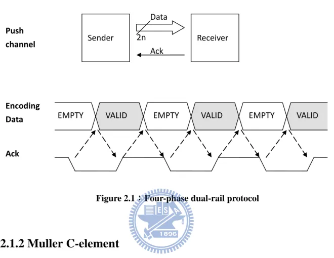
The key point of asynchronous circuits is handshaking protocols. It is responsible to communicates different modules. The most popular protocols are two-phase/four-phase with bundled-data/dual-rail. Our processor is based on four-phase dual-rail protocol which is illustrated in figure 2.1. Four-phase protocol is the common design style due to the simple characteristic. Many asynchronous processors take this design methodology such as CAP (Caltech Asynchronous Processor), FAM (Fully Asynchronous Microprocessor), Strip (A Self-Timed RISC Processor), etc [5]. The company, ARM also developed some commercial products such as ARM996HS [6] and it is based on four-phase protocol.
Dual-rail is one of the data representations, which encodes 1-bit data into 2 wires as shown in table 2.1. For example, if two-wire (Data.t, Data.f) = (0/1, 1/0), it means valid data 0/1. (Data.t, Data.f) = (0, 0) is not a value, and it means empty. Because there is no request signal in dual-rail we use empty to do the action of returning to zero. Although dual-rail increases the cost, it is more robust then single-rail. Most importantly, if we use single-rail, we need to give proper delay everywhere, and it is hard to know it.
Table 2.1 : 1-bit dual-rail encoding
Data.t Data.f Value 0 0 Empty 0 1 Valid 0 1 0 Valid 1 1 1 Not used
5
Figure 2.1 shows the handshake protocol between two modules. We show the detail about data (from sender) and ack (from receiver) relationship in above. Value empty plays the role of returning to zero as difference of continuous valid data.
Figure 2.1:Four-phase dual-rail protocol
2.1.2 Muller C-element
The Muller C-element is a basic element in asynchronous circuits. Table 2.2 shows the truth table of C-element. The symbol of C-element is shown as figure 2.2.
Figure 2.2:The symbol of C-element
Table 2.2 : 2-input C-element
Input1 Input2 Output
0 0 0 0 1 No change 1 0 No change 1 1 1 2n Ack Data
EMPTY VALID EMPTY VALID EMPTY VALID
Encoding Data Ack Receiver Sender Push channel Input 1 Input 2
C
Output6
2.1.3 Dual-Rail Registers
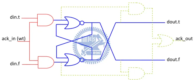
All the registers in our processor are made with dual-rail form. Figure 2.3 shows 1-bit dual-rail register like TITAC’s [7]. The blue portion (thick line) stores data from input data (din.t, din.f). Value (0, 0) does not affect the stored value in blue portion. Therefore, the red portion (solid line) controls writing input data or not. Usually, the wt signal comes from the previous stage. The green portion (dotted line) checks the input data and stored data equal or not, if data is already stored then output ack_out. However, there is no read control in this figure. It is similar to red portion, controlled by AND-gate.
Figure 2.3:1-bit dual-rail register
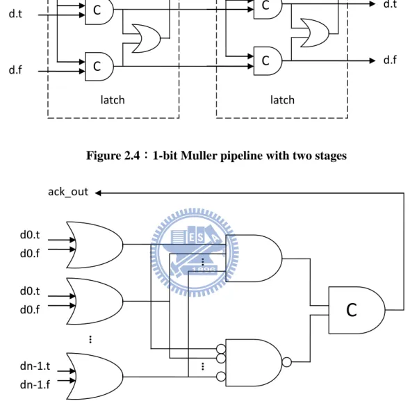
2.1.4 Muller Pipeline
Muller pipeline is based on four-phase dual-rail protocol. In figure 2.4, we can see that the pipeline latch is built of C-element. In the case of many bits, completion detection unit costs a lot by multi-input C-element. So we use alternative one to reduce cost as shown in figure 2.5. Because we put empty token between adjacent valid tokens, the pipeline utilization is 50%, and we already explained it in chapter 2.1.1. In general, completion detector is made by C-element. Due to the expensive cost of multi-input C-element, the
din.t
din.f
ack_in (wt) ack_out
dout.t
7
alterative completion detector is widely used as shown in figure 2.5.
Figure 2.4:1-bit Muller pipeline with two stages
Figure 2.5:Alternative completion detector
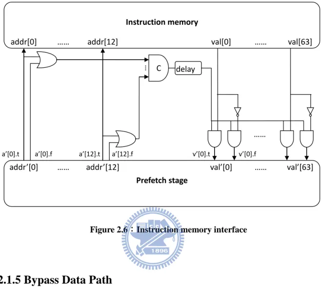
2.1.5 Memory Interface
We use synchronous memory as instruction memory due to the expensive cost of asynchronous memory. Thus we need the memory interface between synchronous and asynchronous circuits as shown in figure 2.6. The multi-input C-element is also replaced by alternative one as figure 2.5 actually.
… … … d0.t d0.f d0.t d0.f dn-1.t dn-1.f
C
ack_out Ack_out d.f d.t Ack_in d.f d.t latch latchC
C
C
C
8
Figure 2.6:Instruction memory interface
2.1.5 Bypass Data Path
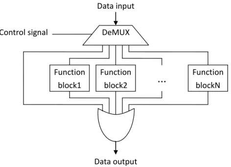
In asynchronous design style, the one of advantages is low power requirement. We gave the example before and the following figure 2.7 shows how it really happened. In this figure, we let data pass through just one function block every time. To the other function blocks, they just pass empty (all data bits are 0) token. The irrelative portions do not waste power obviously. Moreover, if we receive NOP instruction we will just pass it to the next stage without unnecessary calculation. It will be fast and consume less power. It is a practical application about asynchronous design concept.
Instruction memory
addr[0] …… addr[12] val[0] …… val[63]
Prefetch stage
C
addr’[0] …… addr’[12] val’[0] ……
a’[0].t a’[0].f a’[12].t a’[12].f
…
v’[0].t v’[0].f
val’[63] ……
9
Figure 2.7:Bypass Data Path
Data input Function block2 Function block1 Function blockN Control signal Data output
...
DeMUX10
Chapter 3 Related Works
Since RISC VLIW processor has fixed instruction length. In most time, instruction packet is not full utilization. It means that there are many useless NOP instructions occupy the space in instruction packet. But it still needs to be put into instruction memory which causes waste. Moreover, to cut down the program code size implicitly can reduce the communication times between instruction memory and CPU. Thus we can complete a program much quickly. For these reasons, there are numerous studies to deal with the problem what we called instruction compression. We will introduce some general methods briefly in the following.
3.1 Common Instruction Compression
Although instruction compression can reduce wasting memory, it increase hardware cost. Therefore, it is a trade off between memory space and hardware cost. In academic research, they even employ data compression technology with expensive cost. However, commercial processors usually take easy ways.
3.1.1 Data Encoding Scheme
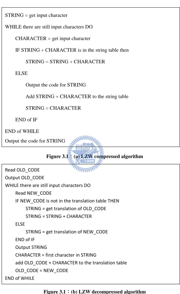
Because the program is also composed of binary code (machine code), some people apply data encoding scheme to instruction compression. The basic idea is to replace original code with fewer bits. The compression ratio is decided by code repeating times. Obviously, it needs to create table which stores the corresponding relation. LZW [8] and Huffman coding are two common data compression methods. In many related papers, instruction compression is based on them [9].
11
Figure 3.1:(a) LZW compressed algorithm
Figure 3.1:(b) LZW decompressed algorithm
STRING = get input character
WHILE there are still input characters DO CHARACTER = get input character
IF STRING + CHARACTER is in the string table then STRING = STRING + CHARACTER
ELSE
Output the code for STRING
Add STRING + CHARACTER to the string table STRING = CHARACTER
END of IF END of WHILE
Output the code for STRING
Read OLD_CODE Output OLD_CODE
WHILE there are still input characters DO Read NEW_CODE
IF NEW_CODE is not in the translation table THEN STRING = get translation of OLD_CODE STRING = STRING + CHARACTER ELSE
STRING = get translation of NEW_CODE END of IF
Output STRING
CHARACTER = first character in STRING
add OLD_CODE + CHARACTER to the translation table OLD_CODE = NEW_CODE
12
LZW:
Lempel Ziv proposed a data compression approach in 1977. Terry Welch refined it later in 1984. The LZW algorithm is shown as following figure 3.1 (a)(b). Like many data compression methods, LZW algorithm looks up translation table as dictionary. But both compression and decompression create translation table respectively. It means that doing decompression just need encoding data without table information, the table will be created automatically. Thus the translation table has dynamic contents and the contents are added step by step. That is why the LZW algorithm suits instruction compression.
Huffman:
We can also apply Huffman scheme to instruction format. The main idea is to analyze the instruction components of some specific application program by benchmark. For example, if we want to compress op code we give the often used instruction type fewer bits and give the seldom used instruction type more bits.
Most data compression methods will let instruction length be variable. In general, these methods are trade-off between compression ratio and area overhead. Besides the expensive cost of data compression methods, commercial products focus on balance. The following approach is another idea with fixed instruction length. The idea is basic on characteristic of VLIW architecture.
3.1.1 Commercial Products
The VelociTI architecture is very long instruction word (VLIW) architecture [10] which is developed by the company of Texas Instruments. Unlike academic research, commercial processor focus on both code size and hardware area cost.
The main idea of instruction compression is to eliminate NOP. The mechanism needs to coordinate instruction format. They use last 1-bit of instruction which is called p-bit to
13
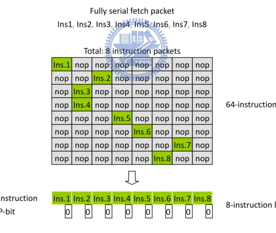
indicate that the instruction is the end of instruction packet whether or not. Therefore it will reduce instruction maximal count. Figure 3.2 (a) shows how it works efficiently in best case. In this case, VLIW architecture is 0% utilization because each instruction packet can only use one function unit. The VLIW processor works like general processor. We can see that useless NOP is 7 times versus valid instruction in each instruction packet. These NOP will not be stored in VelociTI instruction packet so that we compress a great deal of code size. Figure 3.3 (b) shows the worst case and there is nothing happened. The new instruction packet format is same as original one. In general program, the code is impossible to be the form of fully parallel fetch packet. Basically, this mechanism saves plenty space decided by NOP amount.
Figure 3.2:(a) VelociTI instruction packet (best case)
Ins.1 nop nop nop nop nop nop nop nop nop Ins.2 nop nop nop nop nop nop Ins.3 nop nop nop nop nop nop nop Ins.4 nop nop nop nop nop nop nop nop nop Ins.5 nop nop nop nop nop nop nop nop Ins.6 nop nop nop nop nop nop nop nop nop Ins.7 nop nop nop nop nop nop Ins.8 nop nop
Ins.1 Ins.2 Ins.3 Ins.4 Ins.5 Ins.6 Ins.7 Ins.8 0 0 0 0 0 0 0 0 Instruction
P-bit 8-instruction length
64-instruction length Total: 8 instruction packets
Fully serial fetch packet
Ins1, Ins2, Ins3, Ins4, Ins5, Ins6, Ins7, Ins8
14
Figure 3.2:(b) VelociTI instruction packet (worst case)
This method has 50% compression ratio for two-way VLIW architecture under ideal condition. The range of compression ratio between 50% and 60% is great for general processor which is not VLIW architecture. We can see some experimental results on [11] for ARM series architecture.
For ARM, they have a simple way to get compression effect which is called Thumb. This way does not really compress instruction. The original instructions are all in 32-bits length. They expand several 16-bits instructions into original instruction set. These instructions are the copies of original instructions but with shorter instruction formats. Thus it can use these instructions to instead original one when the original instructions do not really need 32-bit length to represent operations. For MIPS, it has the similar way called MIPS16. The way of shorter instruction format will let processor waste time to change mode. For ARC, they have the similar way with mix instruction set. The processors do not need to change mode since the instruction set are variable length.
There are still many special ways to deal with VLIW compression [12]. The instruction with variable length is popular in these years. In [13], it discusses about tradeoffs between decompression overhead and compression ratio. We can see that using more bits only improves compression ratio a little bit. However, we do not take complex method by the reason of double cost (dual-rail encoding scheme) for our asynchronous processor.
Ins.1 Ins.2 Ins.3 Ins.4 Ins.5 Ins.6 Ins.7 Ins.8 1 1 1 1 1 1 1 0 Instruction
P-bit 8-instruction length
8-instruction length Ins.1 Ins.2 Ins.3 Ins.4 Ins.5 Ins.6 Ins.7 Ins.8
Fully parallel fetch packet
Ins1 || Ins2 || Ins3 || Ins4 || Ins5 || Ins6 || Ins7 || Ins8
Ins.1, Ins2, Total: 1 instruction packet
15
Chapter 4 Design for Asynchronous VLIW
processor
In this chapter, we will introduce our asynchronous VLIW processor in the beginning. Then we will show how we implement instruction compression mechanism into this processor in first two stages. We also give instruction set some simple rules to reduce cost. Furthermore, we design a special approach to deal with pc relative instructions. This branch handling method can improve efficient about 50% compared with inserting NOP.
4.1 Processor Architecture
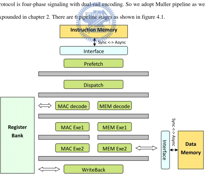
This asynchronous processor is a two-way VLIW architecture. The handshaking protocol is four-phase signaling with dual-rail encoding. So we adopt Muller pipeline as we expounded in chapter 2. There are 6 pipeline stages as shown in figure 4.1.
Figure 4.1:Asynchronous two-way VLIW architecture
Prefetch Dispatch MAC decode MAC Exe1 WriteBack Instruction Memory Interface Sync <-> Async MEM decode MEM Exe1
MAC Exe2 MEM Exe2 Data
Memory In ter face Sy n c < -> As ync Register Bank
16
4.2 Compression implementation
Since we design the asynchronous VLIW processor, we also need to consider saving instruction memory. In chapter3, we already introduced some methods about instruction memory. However, we adopt the VelociTI approach for three reasons.
First, it is simple than the others especially in asynchronous circuits. We know that it is hard to design complexity asynchronous circuits with acceptable cost. It is caused by handshaking protocol especially in four-phase dual-rail protocol. Moreover, if we adopt the complex data compression, it is really hard to design the correct asynchronous circuits without timing constraints. Second, we can take the disadvantage of losing one bit in an instruction format. Finally, simple way gives the processor operates efficiently and the complex one is not worth to do it.
Our processor is a 32-bit RISC processor. Each instruction keeps last one bit for parallel bit. The parallel bit = 1 means it can be parallelly executed with next instruction in two function units. Otherwise, it can only be executed in just one function unit. Although we eliminate the NOP instruction, NOP instruction is still allowed in instruction packet. For example, we can assign a NOP instruction packet like 0x0000000100000000 or 0x00000000. There is no difference between them.
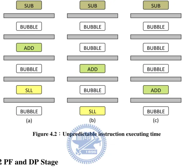
4.2.1 Stage Timing Issues on Asynchronous Circuits
Because there is no clock signal to cooperate with each stage, the time to pass stage is not constant. The adjacent instructions may not be located on corresponding stages. Figure 4.2 shows all possible situations. In this example, the instruction sequence is SLL, ADD and SUB. Case (a) is ideal status with interlaced format that instructions are divided by exactly one bubble; Case (b) and (c) are another situation that add instruction runs fast. In the other hands, we have no idea to know or even predict every stage’s status. It must be take care
17
when we deal with signal across multiple stages.
Figure 4.2:Unpredictable instruction executing time
4.2.2 PF and DP Stage
To deal with instruction decompression, the relative information and instruction buffer is necessary. The buffers are made by registers. Here is the problem about read/write timing. To insure work correctly, our main idea is to separate register read/write into adjacent stage; thus we can promise instruction sequence since there is at least one bubble between two instructions. We use two stages (Prefetch and Dispatch) to complete instruction fetch mechanism. However, if we read/write same register in one stage, we still need to consider read/write timing and the possible solution is to use latch. It is similar way to complete it with two stages.
SUB BUBBLE ADD BUBBLE SLL BUBBLE SUB BUBBLE ADD BUBBLE SLL BUBBLE SUB BUBBLE ADD BUBBLE BUBBLE BUBBLE (a) (b) (c)
18
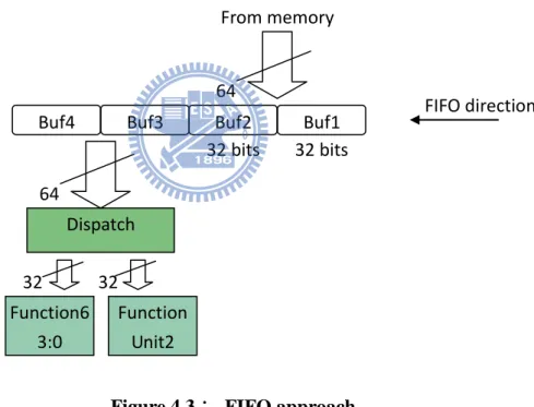
4.2.3 FIFO Approach
In synchronous processor, it is familiar to use FIFO storing tag and buffer as shown in figure 4.3. This mechanism needs at least three steps: load memory, move FIFO and send output. Figure 4.3 is the example of 2-way VLIW and use 4 buffer slots to store instructions. Buf1 and buf2 load from memory and move left to buf3 and buf4. The buf3 and buf4 are waiting for executing. There are two cases: if the instruction packet in buf3 and buf4 can be parallelly executed then send it into dispatch unit and move buf1 and buf2 into buf3 and buf4; if the instruction packet in buf3 and buf4 should be executed along then send one instruction into dispatch unit and rearrange buffer FIFO.
Figure 4.3: FIFO approach
Unfortunately, some case will cause pipeline stalled as illustrated in figure 4.4. Buf1 and buf2 always fetch 2 instructions from memory if they are empty slots. In (b), it does not load from memory. It causes the later step (d) is not ready to send output and the pipeline is stalled. In this example, we assumed sending output to clean slots first, then moving FIFO and loading new instructions. If we exchange the sequence into 1.move FIFO, 2.load new instructions, 3.send output, then the pipeline is still stalled as shown in figure 4.5.
Buf4 Buf3 Buf2 Buf1 From memory Dispatch Function6 3:0 Unit1 Function Unit2 FIFO direction 32 bits 32 bits 64 64 32 32
19
Figure 4.4:Pipeline Stall - 1
Figure 4.5:Pipeline Stall - 2
Buf4 Inst1 Buf3 Inst2 Buf2 Buf1 Buf4 Buf3 Buf2 Buf1 Inst1
Inst2 Inst3 Inst4
(a) (b)
Buf4 Buf3 Buf2 Buf1 Inst2 Inst3
Inst4 Buf4 Buf3 Buf2
(c) (d)
Buf1
X
Inst4 Inst5 Inst6 Inst0
X
X
Buf4 Buf3 Buf2 Buf1
Inst1 Inst2 Inst3 Inst4 Buf4 Buf3 Buf2 Buf1 Inst1
Inst2 Inst3 Inst4
(a) (b)
Buf4 Buf3 Buf2 Buf1 Inst2 Inst3
Inst4 Buf4 Buf3 Buf2
(c) (d)
Buf1
X
Inst5 Inst6 Inst4 Inst5 Inst6 Inst0
X
20
The 3 steps are necessary and whatever you changed the sequence, the stalled situation is still happened. The reason is that the FIFO is not depth enough. However, to increase FIFO depth means increasing overhead. Furthermore, you can notice that it is not really simple for such FIFO mechanism. Actually, it still has another stalled situation. It can move one or more slots to solve the problem [14]. In [14], we can see the FIFO approach has lots overhead with MUX everywhere. However, we proposed the index buffer approach to reduce cost and make it fast.
4.2.4 Index Buffer Approach
Beside the FIFO approach, we use 3 buffer slots to store instructions and we use two stages to implement instruction decompression. The main idea is that if we can choice the source of output instructions, we do not need to move buffers. Thus we reduce the area cost and moving overhead. In figure 4.6, there are 2 stages before the decode stage. In the following, when we indicate something is x bits length, it means x data bits with 2x wires due to the dual-rail implementation.
The first stage (called PF stage) gets instructions (64bits) from instruction memory and puts it into proper buffer according to valid bits (3bits). Valid bits are used to indicate each buffer is empty or not. The second stage (called DP stage) dispatches instructions into the expected sequence.
We load instructions from memory into corresponding buffer with sequence: buf0->buf1->buf2->buf0…. , we use index 2bits to indicate the positions. In fact, to put instructions into proper buffer does not reference index. We can make determination only by valid bits. We just read index in the first stage and pass to the next stage by latch. Index bits are reference by DP stage.
21
Figure 4.6:Index buffer approach
Figure 4.7:Initial status
We will give an example to show how the mechanism works as illustrated in figure 4.7 and figure 4.8. In figure 4.7, instruction 6 and instruction 7 can be parallelly executed and
Instruction Memory
Buf0 Buf1 Buf2
+ nop nop V MAC Decoder L/S Decoder |V|I | PC Index PC Buf0 000 | V | I | PC 00 Buf1 Buf2 Inst.1 Inst.2 Inst.3 Inst.4 Inst.5 Inst.6 Inst.7 Inst.8 Instruction memory 0x00 0x00 0x01 0x02 0x03 Valid | Index | PC PF stage DP stage Decode stage PF latch DP latch PF – read DP - write DP – read PF - write
22
the other can not. What we do is to dispatch the expected instruction sequence before decode stage. The buffer is written by PF stage and is read by PF stage. The tag bits are written by DP stage and are read by PF stage. We assume the valid token and empty token are interlaced between stages in the following figure 4.8(a). To illustrate the instance, we named each token handling step.
Figure 4.8:(a) Continuous single-handled instruction – part I
Buf0 empty Buf1 010 01 0x01 Inst.1 Inst.2 Inst.1 NOP Buf1 Inst.2 empty 010 01 0x01 |010|01 | 0x01 Valid Token Valid Token Buf0 |000|00 | 0x00 Buf1 000 00 0x00 Inst.1 Inst.2 Valid Token empty Buf1 101 10 0x01 NOP Valid Token Inst.2 Inst.3 Inst.4 Inst.2 Inst.3 Inst.4 empty (step 2) (step 3) (step 4) (step 1)
23
Figure 4.8:(b) Continuous single-handled instruction – part II
In step1, the main job is to load instruction memory with pc address. To choice the target position, it read valid bits to reference. Finally, valid bits, index bits and pc are put into the PF-latch. In step2, the value which is in the PF-latch passes to the next stage. The index = 0, so we load instruction from buf0 and buf1. Then we checked the parallel bit of the loaded instruction (buf0) is 0. So we do not take the value of buf1 but insert NOP (0x00000000) to instead. Because we take one instruction from buffer, the index plus one
Buf0 empty 001 00 0x02 NOP empty 001 00 0x02 |001|00 | 0x02 Valid Token Valid Token Buf0 |101|10 | 0x01 101 10 0x01 Valid Token empty 110 01 0x02 NOP Valid Token Inst.4 empty (step 6) (step 7) (step 8) (step 5) Inst.3 Inst.4 Inst.3 Inst.4 Inst.3 Inst.5 Inst.6 Inst.4 Inst.5 Inst.6 Inst.4
24
and write into index register. Since the original valid value is 3’b000, we know we would load new one in the previous step and change it into 3’b011 (v2v1v0). Furthermore, we load one instruction from buffer in this step, change it into 3’b010 and write back to the valid register. In step 4, there are only one empty buffer slot after taking one instruction. So the pc value will not be changed. It cause the buffer content will not be changed in the next step.
Figure 4.8:(c) Continuous instruction
empty 100 10 0x03 NOP empty 100 10 0x03 |100|10 | 0x03 Valid Token Valid Token |110|01 | 0x02 110 01 0x02 Valid Token empty 010 01 0x04 Valid Token empty (step 10) (step 11) (step 12) (step 9) Inst.6 Inst.5 Inst.6 Inst.5 Inst.6 Inst.5 Inst.7 Inst.8 Inst.6 Inst.7 Inst.8 Inst.6 Inst.7
25
In figure 4.8 (b), the step 5 does not load data from instruction memory either put into the buffer since the buffer has no enough space. Therefore, this step is fast to pass than step 1 or step 3.
In figure 4.8 (c), the difference is in step 12. Instruction 6 and instruction 7 can be parallelly executed. Because the parallel bit of instruction 6 is 1, we also load the next instruction ( (index + 1) % 3 = 2’b00 ). To reduce unnecessary overhead, instruction 6 and instruction 7 only can be placed in sequence as figure. The result is not different between Ins.6 | Ins.7 or Ins.7 | Ins.6. In the example, the single-handed instruction is always placed in the left side. However, no matter the instructions are single-handed or not, 3 buffer slots is enough to store them without 2 times memory access.
As we mentioned before, the dispatch stage writes new valid bits and index bits into registers, and the value is referenced by next step. We renew the registers in two steps. Table 4.1 shows the valid bits changing rule. For example, if the current instruction is single-handed (p-bit = 0) and the valid bit (from PF-latch) is 3’b100 the new valid bits will be 3’b011. Because we know we would load instructions into 2 buffers in the previous step and we will take one instruction from buffer. However, v2v1v0 will not be 3’b111 due to the dispatch will consume one instruction at least. By the way, to reference index bits here is unnecessary. Table 4.2 shows the index bits changing rule. Index = (index + 1 + p)%3. However, when tag = 3’b000 it will be reset to 2’b00. The purpose of reset is to maintain the same rule especially the branch happened, we let the mechanism starts from buf0 when the slot are all empty. Furthermore, L-bits is modified by exe1 stage.
26
Table 4.1 : Valid bits changing rule p-bit v2v1v0 1 0 000 000 010 001 100 110 010 001 101 011 000 010 100 010 011 101 000 001 110 000 100 111 111 111
Table 4.2 : Index bits changing rule P index 1 0 0 2 1 1 0 2 2 1 0
4.2.5 Instruction Rules
In fact, we have the instruction rules to decide the function unit in compile time. Not all the instructions can be executed in each function unit but almost. We can see the op code in table 4.3, the memory related instructions can only be executed in MEM function unit. Since if these instructions can be parallelly executed, the memory read/write port will increase and we need to handle the extra dependency problem. This rule makes the circuit much simple.
When the instruction is single-handed, we only compare the first bit and second bit so that we can select the entry of function units. When the bits = 2’b11, the instruction will be put in the right side for MEM function unit. The others are put in the left side for MAC function unit even it also can be executed in the right side. Besides, there is another benefit. For the single-handed instructions, they can be executed in each MAC or MEM function
27
unit. Most of them run fast in the MAC function unit by the lower gate delay of data path. Furthermore we show the possible instruction input types in table 4.4.
Table 4.3 : The op code of 2-way VLIW asynchronous processor
29-27
31-30 000 001 010 011 100 101 110 111
00 NOP R type ADDI ADDIU SUBI XORI WAIT INTERRUPT
01 J SLTI RETURN CALL BEQ BNEQ REPB
10 ANDI ORI ACCLDH ACCLDL
11 LW LH LL LDW SW SH SL SDW
Table 4.4 : Possible instruction inputs combination
Input from buffers Dispatch output (MAC/MEM)
Fn1 Fn1 | NOP
Fn1 | Fn1’ Fn1 | Fn1’ Fn1’ | Fn1 Fn1’ | Fn1
Fn1 | Fn2 Fn1 | Fn2
Fn2 NOP | Fn2
In table 4.4, fn1 means the instruction can be executed in function unit 1 or both two function units. Fn2 means it only can be executed in function unit 2. To simply circuits, we fix Fn1 | Fn1’ in Fn1 | Fn1’. There is no reason to be Fn1’ | Fn1 though it also works. In the other words, we do not have FN (function unit) bit on instruction format to indicate function units.
4.3 Advanced Branch Handling
The general control hazard handling grouped into two types, software solution and hardware solution. The software solution is simple way that inserts enough NOP instructions after branch instruction in compile time. Stalling pipeline is the hardware
28
solution. As we mentioned before, Muller pipeline is 50% utilization. However, we need to pass one instruction in our processor architecture. To insert NOP or stall pipeline will take 2 steps to pass a useless instruction. We design an efficient method that takes characteristic of 50% utilization.
4.3.1 Flush and Stall Methods
In figure 4.9, we assumed that instruction sequence is BEQ, ADDI, SUB……. In flush method, the ADDI instruction will be flushed as NOP instruction. It takes 2 steps (NOP + bubble) to flush it. The improved method changed the original ADDI instruction into bubble, thus finished the action of return to zero. Since we do not have another instruction between BEQ and SUB, there is no more bubble. We save the original bubble, so we make it efficiently.
Figure 4.9:Branch handling methods
In figure 4.10, we show the pc handling part. Since we have buffer to store three instructions, the “pc” in the PF-latch is not the address of current instruction. The pc
BEQ BUBBLE ADDI BUBBLE SUB BUBBLE
BEQ BUBBLE ADDI BUBBLE SUB BUBBLE NOP
X
(a) Flush method
BEQ BUBBLE ADDI BUBBLE SUB BUBBLE
BEQ BUBBLE ADDI BUBBLE
SUB BUBBLE
X
29
value represents the current program counter. We need to calculate the corresponding address therefore and pass to the next stage. To avoid potential problem, we do not process the branch instruction in decode stage but in the next stage, exe1. If we process branch instruction in decode stage, the core may process another instruction in prefetch stage. That means we read/write pc register in the same time. It violated the principle that we said before. Another problem is that the dispatch stage is definitely bubble token when the decode stage is valid token. So we can only flush instruction in prefetch stage. It makes the branch handling much harder.
Figure 4.10:PC selection architecture
However, we send branch target address and stall control signal to dispatch stage from exe1 stage. The stall block is made by AND gate and connect with stall ctl and the dispatch output (instructions before DP-latch). Therefore, the stall ctl can make any instructions here be empty token. We also write the target address to pc register instead of original pc which
Prefetch Dispatch MAC decode MAC Exe1 MEM decode MEM Exe1
…
Stall pc pc+1 PC Buffer I & V | L | V | I | PC | PC’ IT Interrupt request No. PC Calculate PC’ stall ctlbranch target address
pc_mux p c_ m u x2 L location
30
from dispatch stage.
4.3.2 Special Case
For example, our BEQ instruction format is BEQ, rd1, rd2, address, L-bit, P-bit. P-bit is always 0 for branch relative instructions. If rd1 = rd2 then change pc into pc + address. Since 2-way VLIW architecture, each pc address points to 2 instructions. L-bit (1-bit) is used to indicate position. The normal case is L-bit = 1. When L-bit = 0, we select second instruction of target instruction packet, and we should abandon first one. So we actually write the valid bits into 3’b000 (the target instruction is single-handed in this case, so the buffer will all be empty). When L-bit is 0, the compiler should avoid the situation that the target instruction can be parallelly executed. If not, then it needs 2 times of memory access to load these instructions. Therefore, it loses the benefits of parallel executing. In our approach, we assumed that compiler will not let L-bit = 0 and P-bit = 1 in the same time. There are two solutions for compiler. We can force the P-bit of target instruction be 0. Or we can insert NOP to the original target address. However, the problem results from VLIW architecture. The special case needs 2 times memory access basically. So it is unnecessary to handle it by hardware if the compiler can solve the problem.
4.3.3 Different Timing Cases
No matter the branch handling method is, there is a critical issue must be guaranteed, the timing issue. Because of the branch handling is certain to communicate between different stages in pipeline architecture. For our branch handling method, the possible combination of valid token and empty token are shown as figure 4.11. We send branch address and stall control signal in exe1 stage so the exe1 is valid token.There are 3 possible conditions.
31
Figure 4.11:Three possible valid token conditions
Case (a) is an ideal condition and we explained it already. (b) is the case that the instruction which is after branch run slower so that it is still in prefetch stage. In this case, the stall control signal does nothing because it changes empty to empty. Dispatch stage will not receive the signal in the next step obviously. It does not need to flush in the next step anyway. However, the target address still sends to dispatch stage which is empty token actually. The pc_mux will select valid token when the other is empty token so it will write target address to the pc register whatever. Only when all the inputs are valid token then it depends on target address. However, whether the instruction is branch or not, the branch target address should be valid token. Thus we keep the address zero of instruction memory to indicate branch taken or non-taken. If target address is 0, pc_mux will not select address from target address. Case (c) is another special case. It feeds one valid token (branch) first, and feeds next one after finishing handling. Hence it is a simple situation just works like single-cycle machine so that there is no problem.
However, it still has some timing constraints that we referred in chapter 4.6.
(a) (b) (c) Prefetch Dispatch Decode Exe1
E
V
E
V
V
E
E
V
E
E
V
E
32
4.4 Interrupt Handling
As we referred before, this processor will be one core of future multiprocessor. To communicate with another core (or peripherals), we need interrupt handling at least. It is also shown in figure 4.10. Interrupt table is made by registers. It saves the corresponding memory address of interrupt number. When it receives interrupt number from outside pc_mux2 will select the address from interrupt table. After pc changes into interrupt service routine, the routine will save pc and another registers first by push them into memory. After finishing routine, pop them from memory and write back pc.
4.5 Data Flow Chart
Figure 4.12:PC selection flow chart
We show the simple flow chart to expound our design in figure 4.12 and figure 4.13. In
Interrupt No
≠0 Buffer empty slots
≧2
Save pc to pf-latch Yes,
Read pc from IT No,
Read pc from register
Calculate pc’ and save into dp-latch
Yes, pc = pc+1
Branch target address≠0
Write back address to pc register
Yes,
select pc address
No,
select branch target address
No, pc = pc
33
these flow charts, we also mark PF and DP stage and it is helpful to reference figure 4.10. However, the branch target address is from exe1 stage. It is much clearer that we read/write registers in adjacent stages so that there is no register consistent problem. In other words, the stages have one valid token at most in the same time. The empty token let the stage do nothing actually.
Figure 4.13:Instruction selection flow chart
Buffer empty slots ≧2 Put new instructions
into proper buffers Yes
No
Write L, V and I bits into pf-latch Read Pc, L, V and I bits from registers
Interrupt?
Reset V and I bits Select ISR address
Yes
No
Load instructions from memory
Read pf-latch value Read instruction from buffer(P)
L bit = 0?
Reset V and I bits Yes No Calculate new PC, PC’, V and I bits L bit = 0 I = (I +1)%3 P bit of instruction = 1? Read buffer(P+1) Yes No Use NOP instead
Write PC, L, V and I bits into registers
Write instructions and PC’ into DP-latch
34
Sometimes, the source of PC may come from branch or interrupt. We can notice that the interrupt request has higher priority than the others in figure 4.12. Although we use same name like L bit in two stages, but they are actually different. The value comes from register or latch.
4.6 Timing Constraints
Although our design principle is to separate read/write registers into adjacent register. The branch handling is across two or more stages. The L bit is read by Prefetch stage and written by exe1 stage. In the timing model of figure 4.11(b), we do the read/write actions at the same time. But we can change the read/write stage into dispatch/ID stages to solve the problem. There is another essential problem about branch instructions. The value of PC register has two sources from different stages. It may not work correctly.
We assume the time stamp of the instruction which is after branch instruction sending new pc address from dispatch stage is Td. The time stamp of branch instruction sending new
target address from exe1 stage is Tb. It must be guaranteed that Tb > Td in the normal case of
figure 4.11(a). The case (b) and case (c) will not be troubled. One of the possible solution is to handle the branch instruction form exe1 stage to dispatch stage. And use merge to select pc source from adjacent stage due to there is one valid token at most. However, it will make read/write pc register in the same time and cause another timing problem.
Anyway we still can solve the problem by extra circuit. We regard it as future work and we have some discussion in the last chapter.
35
Chapter 5 Simulation Result
5.1 Simulation Environment
In this chapter, we show the working situation by waveform first. Than we give some data analysis about compression ratio and area cost. We use ModelSim to generate waveform and use design compiler to synthesize circuits.
To the waveform, we set each stage has similar delay time to observe stage translation. In general, every signal has interlaced empty token and present data in double line. However the relative signals of synchronous memory have no empty token as shown in figure 5.1. In this figure below, we circled the BEQ instructions with its “long” empty token compared with others.
36
5.2 Compression Ratio Analysis
In table 5.1, we show the compression ratio (compressed code size / original code size) with different program. We write some assembly code with compressed/uncompressed version for our processor as benchmark. We translate two programs to test. FFT is one of general testing program since it is widely used for DSP. The other one is bubble sort which instructions are almost serial executed. Thus it is better case for this compression way.
Besides, our processor needs to insert a NOP when data dependency happened. The compression way will cut half length of NOP instruction from 64bits to 32bits. So the data dependency will be a major effect about compression ratio. To show the impact, we also calculate code size without NOP instructions to observe.
We can see the code size of original assembly code and compressed one in table 5.1. Theoretically, the best compression ratio is decided by the count of VLIW fields. N-way VLIW architecture has
N
1
compression ratio when all instructions can not be parallelly executed. To our test, the FFT is 1032bytes versus 632bytes and the bubble sort is 200bytes versus 112bytes. Since the bubble sort has lower program parallelism, it compressed more than the other one. In this program, we just count main loops without initial part.
However, we did not use loop unrolling or another special compiler technique to both versions. These techniques will raise executed parallelism but also lower compression ratio. Obviously, programs with NOP have better compression ratio as a result of worse ILP (Instruction Level Parallelism).
Table 5.2 : Compression ratio comparison 2-point FFT 2-point FFT
(without NOP)
Bubble sort Bubble sort
(without NOP)
Original 1032 680 200 128 Compressed 632 448 112 80 Compression ratio 61.2% 65.8% 56% 62.5%
37 50 52 54 56 58 60 62 64 66 68 co mpr es si on r at io % 2-point FFT
2-point FFT (without nop) Bubble sort
Bubble sort (without nop)
Figure 5.2:Compression ratio diagram
5.3 Area Report
We use Design Compiler to synthesis circuits under 0.13μm process. The total area consists of cell area and net area. The cell area of decompression portion is only 2.8% of entire processor as shown in table 5.2. The decompression overhead is as small as we expected. We have approximately 200 bits to store data for decompression part. The size of register bank is 32×32×2 bits on the processor. The store unit has 9.8% area ratio. On the other hand, function block size is the great impact on area ratio for our processor.
Table 5.2 : The overhead of decompression area
cell area Total area(μm2) Decompression 26012 (2.8%) 693536 (3.6%)
Processor
(with decompression)
38
Chapter 6 Conclusion and Future Work
In this thesis, we proposed a novel implementation method about VLIW compression for asynchronous processor. The basic concept is to separate data read/write into adjacent stages that can avoid conflict problem. Furthermore, the idea of index buffer can reduce area overhead. We also improved control hazard by hiding branch penalty under Muller pipeline characteristic.
The general VLIW architecture takes logN bits on instruction format to indicate N-way function units. In chapter 4.2.5, we explained how we save function unit bit. In other words, we do not loss one bit (P-bit) for instruction compression. The overhead about instruction compression is only area cost. As simulation result appears, the overhead of cell area is 2.8% of entire processor. The simple way also has satisfied compression ratio about 60%.
However we can further improve this compression mechanism. We notice that we cannot eliminate all NOP instructions since these instructions must exist as a result of data dependency. But these NOP instructions appear in a program very often. We use 32bits NOP to deal with data dependency by original compression method. Thus NOP instruction has 50% compression ratio in this situation. We can further improve it if we change instruction packet from fixed length into variable length. The idea is to use op-code (5bits) instead of full NOP instruction. We fix it into full instruction by hardware. The circuits in the front to detect/fix NOP instructions will not be complex. It just reconstruct instructions after instruction fetch. Thus it has
64
5
compression ratio about NOP instruction for data dependency. The entire improvement is decided by the frequency of data dependency. In this way, the NOP has no end-bit since it must be a complete instruction packet so we can fix it. It is also implicit another compressed chance. Some instruction cannot be parallelly executed with another instruction like BEQ, BNEQ, LW/SW ……etc. However we can also mix both 16-bit and 32-bit instructions into our instruction set.
39
In the previous section, we discussed the timing constraints for the reason of different pc sources. Thus the key to solve the problem is to let pc sources from same stage. The suitable stage is Dispatch in our processor. If we handle branch in Dispatch stage the timing problem will be solved. Of course, Dispatch is the previous stage of Decode. The practice way is to pre-decode branch in particular. It needs to store branch target address in Dispatch stage and determine to branch or not in next stage (Decode stage). Thus it will finish branch instructions in adjacent stages. This way will solve the problem effective even this solution will cause extra overhead. However, control hazard still can be solved by compiler with penalty. Compiler could insert NOP after branch instruction.
40
References
[1] J. Sparsø and S. Furber, Principles Of Asynchronous Circuit Design A Systems Perspective, Kluwer Academic Publishers, London, 2001.
[2] J.D Garside, S.B. Furber, S. Temple, J.V. Woods, “The Amulet chips: Architectural Development for Asynchronous Microprocessors,” IEEE International Conference on Electronics, Circuits, and Systems, Dec. 2009, pp.343-346
[3] S. Hauck, “Asynchronous design methodologies: an overview,” Proceedings of the IEEE, Vol. 83, Issue 1, Jan. 1995, pp.69-93
[4] David Geer, “Is it time for clockless chips? [Asynchronous processor chips],” Computer, Vol. 38, Issue 3, March. 2005, pp.18-21
[5] Tony Werner, Venkatesh Akella, “Asynchronous processor survey,” Computer, Vol. 30, Issue 11, Nov. 1997, pp.67-76
[6] Arjan Bink, Richard York, “ARM996HS: The first licensable, clockless 32-bit processor core,” Micro IEEE, Vol. 27, Issue 2, March-April. 2007, pp.58-68 [7] A. Takamura, M. Kuwako, M. Imai, T. Fujii, M. Ozawa, I. Fukasaku, Y. Ueno, T.
Nanya, “TITAC-2: an asynchronous 32-bit microprocessor based on scalable-delay-insensitive model,” Proceedings of International Conference on Computer Design, Oct. 1997, pp.288-294
[8] Mark Nelson, “LZW Data Compression,” Dr. Dobb’s Journal, October, 1989
[9] Chang Hong Lin, Yuan Xie, Wayne Wolf, “LZW-Based Code Compression for VLIW Embedded Systems,” Design, Automation and Test in Europe Conference and Exhibition, Vol. 3, Feb. 2004, pp.76-81
[10] Seshan N, “High VelociTI processing [Texas Instruments VLIW DSP architecture] ,” Signal Processing Magazine, IEEE, Vol. 15, Issue 2, Mar. 1998, pp.86-101, 117
41
[11] Yuan-Long Jeang, Jen-Wei Hsieh, Yong-Zong Lin, “An efficient instruction compression/decompression system based on field partitioning,” Circuits and Systems, Vol. 2, Aug. 2005, pp.1895-1898
[12] Guido Araujo, Paulo Centoducatte, Rodolfo Azevedo, Ricardo Pannain, “Expression-tree-based algorithms for code compression on embedded RISC architectures,” IEEE Transactions on VLSI Systems, Vol. 8, Oct. 2000, pp.530-533 [13] Yuan Xie, Wayne Wolf, Haris Lekatsas, “Compression ratio and decompression
overhead tradeoffs in code compression for VLIW architectures,” Proceedings of International Conference on ASIC, Oct. 2001, pp.337-340
[14] Kai-Ming Yang, “Improving the Fetching Performance of Instruction Stream Buffer for VLIW Architectures with Compressed Instructions,” National Sun Yat-Sen University, Master Thesis Department of Electrical Engineering, July 2006