This content has been downloaded from IOPscience. Please scroll down to see the full text.
Download details:
IP Address: 140.113.38.11
This content was downloaded on 28/04/2014 at 08:42
Please note that terms and conditions apply.
The Combined Effects of Nitrogen Implantation at S/D Extension and N2O Oxide on 0.18 µm
N- and P-Metal Oxide Field Effect Transistors (MOSFETs)
View the table of contents for this issue, or go to the journal homepage for more 1999 Jpn. J. Appl. Phys. 38 L1366
(http://iopscience.iop.org/1347-4065/38/12A/L1366)
Jpn. J. Appl. Phys. Vol. 38 (1999) pp.L1366–L1368 Part 2, No. 12A, 1 December 1999
c
°1999 Publication Board, Japanese Journal of Applied Physics
The Combined Effects of Nitrogen Implantation at S/D Extension and N
2O Oxide
on 0.18
µm N- and P-Metal Oxide Field Effect Transistors (MOSFETs)
Tien-Sheng CHAO1, Sun-Jay CHANG2, Chao-Hsin CHIEN2, Horng-Chih LIN1, Tiao-Yuan HUANG1,2and Chun-Yen CHANG1,2
1National Nano Device Laboratories, Hsinchu 300, Taiwan, R.O.C.
2Institute of Electronics, National Chiao-Tung University, Hsinchu 300, Taiwan, R.O.C. (Received August 2, 1999; accepted for publication October 27, 1999)
The combined effects of N2-implantation at S/D extension and N2O oxide on 0.18µm n- and p-Metal oxide field effect
transistors (MOSFETs) were investigated. It is found that for n-channel transistors, Vth roll-off and drain-induced barrier
lowering (DIBL) are enhanced by nitrogen incorporation through either N2O oxide or N2-implantation. However, for p-channel
transistors, opposite trends are observed for N2O oxide and N2-implantation. Finally, nitrogen incorporation by either method
is found to improve the interface quality for nMOSFETs. While for p-channel transistors, best results are obtained by the combined effects of N2O oxide and N2-implantation.
KEYWORDS: nitrogen, N2O, MOSFETs, S/D extension
L1366
1. Introduction
Recently nitrogen implantation received lots of attention in the fabrication of deep sub-micron devices.1–3) Nitrogen was proposed to be co-implanted into BF+2-implanted p+ -poly-Si gate to suppress the boron penetration,1) or into the
source-drain region to improve the junction leakage,2)or into
the channel region to improve the n-channel device perfor-mance.3) Meanwhile, N
2O oxide has also been proposed as
a promising gate oxide material for deep sub-micron de-vices.4, 5) Devices with N
2O oxide were shown to exhibit
better hot-carriers immunity, lower charge trapping, higher breakdown field, and better radiation hardness over the con-ventional O2 oxide. It is also known that nitrogen can form
complex with boron in the BF+2-implanted p+-poly-Si gate, resulting in the retardation of boron diffusion.1)On the other hand, nitrogen implanted into the p-type silicon substrate re-duces the activated boron concentration.3)While for N2O
ox-ide, it is known that some nitrogen is incorporated at the SiO2/Si interface and forms strong Si–N bonds. These strong
Si–N bonds are more resistant to hot-carrier degradations over the Si–H and Si–OH bonds. In this paper, we report, for the first time, the combined effects of nitrogen implantation at S/D extension and N2O gate oxide on 0.18µm n- and
p-channel metal oxide field effect transistors (MOSFETs).
2. Experimental
Both n- and p-channel 0.18-µm MOS transistors were fab-ricated. After growing a 4 nm-thick gate oxide in either N2O
or O2ambient at 900◦C for 40 minutes, an in situ
phorsphous-doped n+-poly-Si and an undoped poly-Si layer, both with a thickness of 200 nm, was deposited on n- and p-channel MOSFETs, respectively. The incorporated nitrogen concen-tration for N2O processing is less than 1 at%. Poly-Si films
were etched by an electron cyclotron resonance (ECR) etcher using HBr: O2(50: 1) as etchants. Low-energy implantation
of As+(10 keV, 4×10¹⁴/cm2) and BF+
2 (10 keV, 1×10 15/cm2)
was then employed to form the shallow S/D extension region for n- and p-MOSFETs, respectively. Some splits received an additional nitrogen implantation of 10 keV at a dosage of 5× 10¹³/cm2 and 1× 10¹⁴/cm2 for n- and p-MOSFETs,
respectively, in order to study the effects of nitrogen im-plantation at the S/D extension on the transistor
character-Fig. 1. The Vthroll-off characteristics for nMOSFETs. Insert shows the drain-induced-barrier-lowering (DIBL) characteristics, measured at drain current of 1µA/µm and drain voltage at 1.5 and 0.1 V.
istics. A 150 nm-thick tetraethoxysilane (TEOS) layer was then deposited and reactive ion etching (RIE)-etched to form the sidewall spacer. Afterwards, As+(20 keV, 5× 10¹⁵/cm2) and BF+2 (10 keV, 6× 10¹⁵/cm2) were implanted to form the S/D regions for n- and p-MOSFETs, respectively. Finally, wafers were annealed at 800◦C for 20 min and underwent a rapid thermal annealing (RTA) process at 1050◦C for 20 s for dopant activation.
3. Results and Discussion
Vthroll-off characteristics for n-channel transistors are
dis-played in Fig. 1. The split that received both N2O oxide and
N2-implantation at S/D extension (i.e., N2O oxide+ N2)
ex-hibits the largest, while the control split (i.e., O2oxide only)
exhibits the smallest Vth roll-off. This is due to the
com-bined effects of interface nitrogen incorporation both at the active channel region and S/D extension region. It has been reported that, due to implant-induced defects at the source-drain region, enhanced boron diffusion from the sub-surface punch-through-stopper-implant region to the silicon surface
occurs at regions close to the source-drain edge. This en-hanced boron diffusion results in a net increase in surface boron concentration close to the source-drain edge, causing the so-called “reverse short-channel effect (RSCE)”.6)Since
this defect-induced enhanced boron diffusion is suppressed by the nitrogen incorporation,7) boron redistribution is
sup-pressed. Consequently, the RSCE is minimized, and the tran-sistors display an enhanced Vth roll-off in return. This,
to-gether with the fact that the split which received O2oxide and
N2-implantation at S/D extension (i.e., O2 oxide+ N2)
dis-plays the second largest Vthroll-off, suggests that nitrogen
in-corporation at the S/D extension is very effective in reducing the RSCE effect. This trend is consistent with recent results on MOSFETs fabricated with nitrogen implantation prior to growing the gate oxide,8)and N
2O nitrided gate oxide.9)The
drain induced barrier lowering (DIBL) effect is plotted in the insert of Fig. 1. It can be seen that splits with N2-implantation
show a larger DIBL than those without N2 implantation as
channel length is smaller than 0.25µm, confirming again that nitrogen incorporation at the S/D extension is very effective in reducing the RSCE.
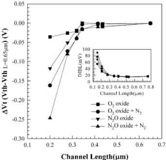
The results on the Vth roll-off for pMOSFETs are shown
in Fig. 2. It is interesting to note that while splits with N2
-implantation at S/D extension show a larger Vthroll-off, splits
with N2O oxide show instead a smaller Vthroll-off. This
inter-esting behavior (i.e., N2O oxide and N2-implantation at S/D
extension do not result in similar Vthroll-off trend, as in the
case of n-channel transistors) can be explained by the boron penetration effects from the p+-poly-Si gate for pMOSFETs. Since N2O oxide is known to prevent boron penetration from
p+-poly-Si gate into the active channel region, a higher n-type channel surface concentration can be preserved, compared to samples with O2oxide. Consequently, the Vthroll-off is
sup-pressed.
To evaluate the polysilicon depletion effect due to boron penetration from the BF+2-implanted p+-poly-Si gate, quasi-static C –V measurements were conducted. The average val-ues of the normalized Cinv/Cox(curves not shown) are 0.931,
0.929, 0.917, and 0.915 for N2O+ N2, N2O, O2+ N2, and
O2 oxide samples, respectively. These data seem to suggest
that nitrogen incorporation can somehow improve the deple-tion effect of the BF+2 implanted p+-poly-Si gate. The in-terface quality of nMOSFETs was analyzed by using charge pumping current measurement, and the results are shown in Fig. 3. Split with O2 oxide but without N2 implantation at
the S/D extension has the largest charge pumping current. This implies that the interfacial quality of the sample can be improved by nitrogen incorporation, introduced either at the SiO2/Si interface by N2O oxide or at the S/D extension by
N2-implantation. It is also interesting to note that splits with
N2-implantation at the S/D extension, irrespective of whether
it received O2 or N2O oxide, show almost identical charge
pumping current, suggesting that N2-implantation at the S/D
Fig. 2. Vthroll-off characteristics for pMOSFETs.
Fig. 3. Charge-pumping current for nMOSFETs under stressing at a drain bias of 3 V. Gate voltage is biased to yield maximum substrate current.
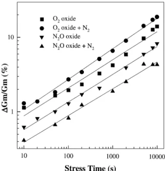
Fig. 4. Transconductance degradation for pMOSFETs under stressing at a drain bias of−3 V. Gate voltage is biased to yield maximum gate current. Jpn. J. Appl. Phys. Vol. 38 (1999) Pt. 2, No. 12A T.-S. CHAOet al. L1367
and N2-implantation at the S/D extension has the lowest Gm
degradation among the four splits used in this study.
4. Conclusion
N2O oxide and nitrogen implantation at the S/D
exten-sion are found to have different effects on 0.18µm n- and p-MOSFETs. For nMOSFETs, Vthroll-off and DIBL effect
are enhanced by nitrogen incorporation, either through N2O
oxide or N2-implantation at S/D extension. While for
pMOS-FETs, N2O oxide and N2-implantation at S/D extension cause
opposite effects in Vthroll-off, which can be explained by the
reduced boron penetration in the case of N2O oxide. Nitrogen
alone is very effective in improving the interfacial quality. Figure 4 shows the transconductance (Gm) degradation of pMOSFET after 10000 s stressing at a drain bias of −3 V with the gate biased to yield the maximum gate current. It can be seen that while nitrogen implantation at the S/D exten-sion alone worsens the hot-carrier degradations for samples with O2 oxide, devices with N2O oxide perform better than
O2oxide. More importantly, split with combined N2O oxide
L1368 Jpn. J. Appl. Phys. Vol. 38 (1999) Pt. 2, No. 12A T.-S. CHAOet al.
incorporation is also found to improve the interfacial quality in nMOSFETs. While for pMOSFETs, the combined effects of N2O oxide and N2-implantation result in the best
perfor-mance in terms of reduced poly-depletion effects and better hot-carrier resistance.
1) T. S. Chao, M. C. Liaw, C. H. Chu and C. Y. Chang: Appl. Phys. Lett. 69 (1996) 1781.
2) T. Kuroi, S. Shimizu, A. Furukawa, S. Komori, Y. Kawasaki, S. Kusunoki, Y. Okumura, M. Inuishi, N. Tsubouchi and K. Horie: 1995 Symp. VLSI Technology, p. 19.
3) A. Furukawa, Y. Abe, S. Shimizu, T. Kuroi, Y. Tokuda and M. Inuishi: 1996 Symp. VLSI Technology, p. 62.
4) G. Q. Lo and D. L. Kwong: IEEE Electron Device Lett. 12 (1991) 175. 5) L. K. Han, D. Wristers, J. Yan, M. Bhat and D. L. Kwong: IEEE Electron
Device Lett. 16 (1995) 319.
6) M. Hane and H. Matsumoto: IEEE Trans. Elec. Device 40 (1993) 1215. 7) H. Hwang, W. Ting, B. Maiti, D. L. Kwong and J. Lee: Appl. Phys. Lett.
57 (1990) 1010.
8) C. T. Liu, Y. Ma, J. Becerro, S. Nakahara, D. J. Eaglesham and S. J. Hillenius: IEEE Electron Device Lett. 3 (1997) 105.
9) C. S. Lai, T. S. Chao, T. F. Lei, C. L. Lee, T. Y. Huang and C. Y. Chang: Jpn. J. Appl. Phys. 37 (1998) 5507.