A Controller for Liquid Crystal Displays in Logic
Analyzers and Oscilloscopes
K. G. Panikumar and T. N. Ruckmongathan
Abstract—Design and development of a controller to display multiple waveforms using liquid crystal displays (LCDs) is pre-sented. The controller generates the column signals directly from samples of the waveforms. A low cost passive matrix display with simple drive electronics for Logic Analyzers and Oscilloscopes is demonstrated.
Index Terms—Controller, liquid crystal displays (LCDs), multi-line addressing, restricted pattern, waveforms.
I. INTRODUCTION
D
ISPLAYS in Oscilloscopes, Logic Analyzers, as well as Electrocardiographs are primarily used for displaying waveforms. Capability to display graphics and alphanumeric information is an advantage, but it is not essential for these products. Liquid crystal displays (LCDs) exploiting the intrinsic nonlinear electro-optic characteristics of the display are called as passive matrix LCDs. They are simple to manufacture and cost less as compared to active matrix LCDs with a nonlinear element incorporated in each pixel. Design and development of a simple controller for passive matrix LCDs is presented in this paper.II. BACKGROUND
Contrast in a passive matrix displays depend on the selection ratio, as well as the steepness of the electro-optic characteristics. Selection ratio is defined as the ratio of rms voltage acrossON pixels to that acrossOFFpixels in the display. A high selection ratio ensures good contrast even when the electro-optic char-acteristics is not steep as in the case of twisted nematic (TN) LCDs. Super twisted nematic (STN) LCDs on the other hand have steep electro-optic characteristics but their response times are about a few hundred milliseconds. TN LCDs have response times in the range of tens of millisecond and are better suited for applications like oscilloscopes. Shanks and Holland [1] have exploited the correlation properties of pseudo random binary se-quences (PRBS) to display a waveform on LCDs. Just one pixel in each column is OFFand it is a point on the waveform. All other pixels in the display are driven toONstate and they are background pixels. This technique has an infinite selection ratio. However, it is not suitable for displaying multiple waveforms.
Manuscript received January 17, 2005; revised June 16, 2005.
K. G. Panikumar was with Raman Research Institute, Bangalore 560 080, India. He is now with Display Institute, National Chiao Tung University, Hsinchu 300, Taiwan, R.O.C. (e-mail: [email protected]).
T. N. Ruckmongathan is with the Raman Research Institute, Bangalore 560 080, India (e-mail: [email protected]).
Digital Object Identifier 10.1109/JDT.2005.853353
A technique [2] based on line by line addressing can be used to display multiple waveforms (restricted patterns). Waveforms are mostly single valued functions of time. Hence, the number of pixels on the waveforms in each column is equal to the number of waveforms that are displayed. This fact is exploited to achieve a selection ratio that is independent of the matrix size.
for restricted patterns
(1) It depends on the number of waveforms that are displayed. Although finite, the selection ratio of restricted pattern ad-dressing is much higher than that of general pattern adad-dressing [3]. Hence, TN LCDs can be used even when the matrix size is very large.
(2) Here, is the number of address lines in a matrix display and
usually . The parameter gives the
number of lines to be multiplexed when displaying general pat-terns so that the selection ratio is equal to that of (1) i.e., re-stricted pattern addressing for displaying multiple waveforms [2]. For example, the selection ratio of restricted pattern ad-dressing technique when displaying four waveforms is equal to that of multiplexing nine lines to display general patterns. Wave-forms can be displayed with a high resolution since; the selec-tion ratio is independent of the matrix size. It could be as large as 1024 1024. However, the supply voltage of the drive elec-tronics increases with the number of lines multiplexed and this imposes a limit on the matrix size. A lower supply voltage that is independent of the matrix size can be achieved if all the rows in the matrix display are selected simultaneously [4]. The supply voltage depends on , the number waveforms. An or-thogonal matrix based on PRBS was used to obtain the selection ratio in (1) while displaying multiple waveforms [5]. However, the number of voltage levels in the column waveforms of the addressing technique increases with the number of waveforms being displayed. This increases the hardware complexity of the column drivers for the matrix display. The number of voltage levels and, hence, the hardware complexity of column drivers can be reduced by selecting a few rows at a time [6]. This tech-nique is reviewed briefly in the next section.
A. Restricted Pattern Addressing Based on Selecting Multiple Address Lines
Restricted Pattern Addressing is based on scanning the dis-play by selecting a few rows at a time, a method that is popu-larly known as multi-line addressing (MLA). Here, the rows in a matrix display are divided into nonintersecting
sub-groups, with rows in each subgroup . A set of
waveforms based on orthogonal functions is used to select rows (address lines) in a subgroup. Simple orthogonal functions like Walsh functions are preferred since it is easy to generate the row and column waveforms. The number of background pixels in each column of the display is , when waveforms are displayed. Selection ratio is independent of the matrix size when the data voltage for the background pixels is assigned to be zero. The data assigned to the selected pixels may be either a plus one or minus one. Assigning a plus one to the selected pixels drives them toOFFstate and achieves a higher selection ratio. Here, the selected pixels get a lower rms voltage as compared to the background pixels. For the sake of understanding this tech-nique, one can assume that the image of waveforms (as it should appear on the display) is stored in a bit map memory. Sampled values of the waveforms are stored and a bit map memory is not necessary as explained under design of a controller in the next section. Column voltage that is applied to each column is proportional to the dot product of a select pattern and the data pattern to be displayed in the selected subgroup. Columns of the orthogonal matrix are referred to as the select patterns. Column voltages for all the columns in the matrix are determined inde-pendently. Voltages (either or ) corresponding to the elements of select pattern are applied to the rows in the selected subgroup. Voltage applied to the nonselected rows is an average of the two select voltages. Row and column voltages are ap-plied simultaneously to the matrix display for the duration . This process is repeated by selecting another subgroup with a different select pattern. A cycle is complete when all the sub-groups are selected once, with all the select patterns. The dis-play is refreshed continuously by repeating this cycle.
In logic analyzers, it is preferable that waveforms do not intersect or overlap and are equally spaced. If this condition is enforced, then the number of voltage levels in the column waveform can be reduced considerably by a proper choice of the number of rows in the subgroups. Fig. 1 shows the column waveforms, when the number of rows in a subgroup is 8, 16, 32, and 64 in a matrix display with 64 rows. Just two voltage levels are adequate in the column waveforms while displaying four waveforms when , as compared to five voltage levels when all the rows are selected simultaneously. The number of voltage levels in the column waveform is just two when one and only one waveform is displayed in each sub-group of the matrix display. The maximum number of voltages in the column waveforms is and this occurs whenever the samples of all waveforms cluster in a subgroup. The techniques for displaying multiple waveforms are compared in [6] based on the number of voltage levels in the column waveforms and the supply voltage. The waveforms in Logic analyzers and electrocardiographs need not overlap or cluster in a subgroup. Hence, the hardware complexity of the column
Fig. 1. Columns waveforms, when the subgroup size is 8, 16, 32, and 64. (a)s = 8. (b) s = 16. (c) s = 32. (d) s = 64.
drivers and, consequently, the power dissipation as well as the cost of the drivers could be reduced by selecting a few rows at a time. This reduction is significant since the number of column in the display is large. Supply voltage is also less as compared to that of line-by-line addressing and it is an advantage in portable products.
III. DESIGN OF ACONTROLLER
A. Block Diagram
A simple block diagram of a display system is shown in the Fig. 2. The waveforms to be displayed are stored in the wave-form memory. Several orthogonal matrices are stored in the row select pattern generator. The column signal generator (CSG) computes the data for the column driver while the subgroup se-quencer (SGS) determines the sequence in which the subgroups are selected. The voltage level generator (VLG) is necessary to generate the various voltages that are used in the row and column drivers. The control logic generates all the control sig-nals necessary to scan the display and refresh it periodically at the rate of about 50 Hz. to avoid flicker. A detailed block di-agram of the drive electronics for a 64 64 matrix display is shown in Fig. 3.
B. Waveform Memory
Sampled waveforms are stored in the waveform memory.
Each sample has to be stored using bits so that
the waveform may be displayed to the highest resolution of a matrix display with rows. Hence, bits are necessary to display waveforms. This is less than , since . Hence, it is preferable to store the samples of the waveform
Fig. 2. Block diagram of the display system.
Fig. 3. Detailed block diagram of the prototype.
without generating a bit mapped image of it. For example, the size of the bit-mapped memory is 307 200 bits for a 640 480 matrix LCD. However, one just needs 46 080 (i.e., ) bits when eight waveforms are stored with 9-bit resolution that is necessary for a matrix display with 480 rows.
C. Row Select Pattern Generator
A row select pattern generator has been implemented using an electrically programmable read only memory. Several orthog-onal matrices are stored in it. Any one of these matrices can be used to scan the display. Elements of these orthogonal matrices are either 1 or 1 and hence one bit is used to store each el-ement. An orthogonal matrix (8 8) obtained by adding a row and column of 1 to a 7 7 matrix consisting of a PRBS of length 7 and its shifted version is shown in (3). A select pattern,
i.e., a column of the orthogonal matrix is accessed in parallel by using an appropriate address from the control logic.
(3)
D. Subgroup Sequencer
The subgroup sequencer determines the order in which the subgroups are selected. A subgroup sequencer is a ring counter
of length or a digital decoder with outputs as
Fig. 4. Schematic diagram of a simple column signal generator. TABLE I
E. Column Signal Generator (CSG)
Column signal generator computes the dot product of the row select pattern and the data in the selected subgroup. The data of the background pixels is zero. Hence, the corresponding ele-ments in the select pattern will not contribute to the dot product. Design of the controller is simple when the number of rows in a subgroup is chosen to be equal to an integer power of
two ( , where , etc.). Block diagram of the
CSG that uses the samples of the waveform to compute the dot product is shown in Fig. 4. An up/down counter is used to compute the dot product. This counter is reset (or preset to a value) before computing the column signal for each column. A sample of the waveforms is represented by
bits after scaling the waveforms and adding a dc offset to po-sition the waveform, as desired by the user. The most
signifi-cant bits point to the subgroup that has
a sample, i.e., point on the waveform. A comparator compares these most significant bits with the address of the subgroup that will be selected. In case they are not the same then the up/down counter is left intact. A ‘true’ at the comparator indicates that the sample point lies in the selected subgroup. The least signif-icant ‘i’ bits are used as the select input of a multiplexer to extract the element in the select pattern that corresponds to row that will display the sample i.e., point on the waveform. The up/down counter is incremented when this bit is logic ‘0’ (corresponds to 1) and is decremented when the bit is logic ‘1’ (corresponds to 1) since the data assigned to a point on the waveform is 1. This process is repeated with samples of all the waveform and final content of the up/down counter is the column signal that is the dot product. It is important to note that the choice of a preset state of the counter could be arbitrary. All one needs to ensure is that the counter is preset to any one state and the voltages applied to the column correspond to the appro-priate dot product values.
Fig. 5. Timing diagram for the column signal generator for displaying four waveforms.
Fig. 6. Schematic of a row driver printed circuit board.
Table I shows the counter states and the corresponding column voltage levels when the preset states are chosen to be 011 and 000. The comparator output is used to enable the counter. The output from the digital multiplexer is used to control the up or down mode of the programmable counter. For a given row select pattern clock pulses are provided to compute the column data from w sampled data corresponding to the waveforms for each column. After computing the column data using clock pulses, the column data is shifted into the column driver card. The counter is again preset to the initial value. The column data for the rest of the columns are computed by repeating the process and are shifted in to the column driver for driving the matrix LCD. Hence,
time intervals are necessary to generate all the column data when subgroup is to be selected with a row select pattern.
Fig. 7. Schematic of a typical column driver used for 642 64 matrix LCD for displaying four waveforms while selecting 16 rows at a time.
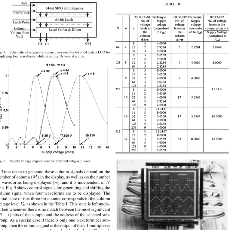
Fig. 8. Supply voltage requirement for different subgroup sizes.
Time taken to generate these column signals depend on the number of column in the display, as well as on the number of waveforms being displayed , and it is independent of or . Fig. 5 shows control signals for generating and shifting the column signal when four waveforms are to be displayed. The initial state of this three-bit counter corresponds to the column voltage level as shown in the Table I. This state is left undis-turbed whenever there is no match between the most significant bits of the sample and the address of the selected group. As a special case if there is only one waveform per sub-group, then the column signal is the output of the s:1 multiplexer and the up/down counter may be replaced with a latch. The latch is reset to start with and the output of the multiplexer is transferred to the latch for shifting into the column driver. In summary, the column signal generator has a bit com-parator, a multiplexer, and an Up/Down binary counter. The number of bits in this counter depends on the number of waveforms to be displayed.
F. Row Driver
MLA techniques have three voltage levels in the row wave-forms. The voltages and are used to select the rows in a subgroup and the nonselected rows are connected the voltage , a voltage that is an average of and . The schematic diagram of a row driver card is shown in Fig. 6. Voltages cor-responding to the -bit select patterns are obtained by using a 2:1 analog multiplexer for each bit of the select pattern. These
TABLE II
Fig. 9. Photograph of a 642 64 TN LCD displaying four waveforms and driven by selecting 16 rows at a time.
multiplexers select either a or depending on the cor-responding element of the select pattern. Outputs from these
multiplexers i.e., and from
the voltage level generator are connected to all the subgroup blocks. Each subgroup block has 2:1 multiplexers, the control input of these multiplexers are grouped together and connected to the corresponding output of the subgroup sequencer.
Sub-group sequencer has outputs
to control the sequence in which the subgroups are selected. Just one output of the subgroup sequencer is high at a time. Hence, the corresponding subgroup is selected with the voltage levels or corresponding to the elements of the select pattern.
Fig. 10. Plot of rms voltage across pixels, and selection ratio versus supply voltage.
The rows in the other subgroups are connected to the voltage . The number of 2: 1 analog multiplexers in the row
driver board is .
G. Column Driver
The complexity of the column driver depends on the appli-cation. Waveforms displayed in an oscilloscope may cross each other or all the waveforms may fall in the same subgroup in some region. Number of voltage levels in the column waveforms is . In case the waveforms do not overlap as in dis-plays of logic analyzers and electro-cardiographs, the number of subgroups can be chosen to be equal to the number of wave-forms. Then the column waveform has just two voltage levels [as shown in Fig. 1(b)] and standard drivers could be used. We have demonstrated this possibility and the schematic of a column driver (SED 1180) is shown in Fig. 7.
H. Control Logic
The control logic generates timing and control signals to sequence and synchronize the flow of information from the memory to the display as dictated by the addressing technique. Address as well as control signals to the row select pattern and waveform memories, shift clock and latch pulse to the drivers, control signal to subgroup sequencer etc. are generated in the control logic. It also ensures that the display is refreshed continuously at about 50 Hz to avoid flicker.
The controller has been implemented on a Complex Pro-grammable Logic Device (CPLD) using VHDL codes. It occupies about 60% of the CPLD having 128 logic cells and 2500 usable gates.
IV. RESULTS ANDDISCUSSION
The feasibility of reduction in hardware complexity of the drive electronics has been demonstrated using TN LCD. The
se-lection ratio is independent of the number of rows and columns in the matrix display. It depends on the number of waveforms that are being displayed. Steepness of the electro-optic charac-teristics of typical liquid crystal mixtures are adequate to multi-plex about 50 rows using the techniques for displaying general patterns. This implies that up to 16 waveforms (i.e., ) can be displayed without any compromise in the contrast ratio that can be achieved. There is no limit on the size of the trix display from the point of contrast ratio. However, the ma-trix size will be determined by the pitch of the interconnections from the drivers to the display and the supply voltage of the drive electronics. The supply voltage for the driver is calcu-lated and measured for different values of subgroup size for dis-playing four waveforms. Saturation voltage for the liquid crystal mixture we used was measured using single pixel electro-optic setup. The (voltage at 90% of the maximum transmission) for the mixture we used is 2.66 volts. Using the waveform erator “WFG 500”, the row and column waveforms were gen-erated and applied to a single pixel electro-optic setup. Fig. 8 shows the power supply requirement for driving 64 64 matrix LCD while displaying four waveforms with different subgroup size.
In case four waveforms (nonoverlapping) are displayed by se-lecting (N/4) rows simultaneously then the number of voltage levels in the column waveform is just two. This is the min-imum number of voltages in any addressing technique. Hence, the complexity of the column driver is lower. On the other hand, there are voltage levels in the column waveform when all the rows are selected simultaneously (PRBS techniques). It is possible to have just two voltage levels in the column wave-forms when Restricted Pattern Addressing Technique (RPAT) [2] based on line-by-line addressing is employed but the supply voltage for the drivers is high. Although the supply voltage could be reduced by about 50% by using a technique similar to the conventional improved Alt and Pleshko technique IAPT [7],
Fig. 11. Typical addressing waveforms when sixteen rows are selected simultaneously to drive a 642 64 matrix display. (a) & (b) row and column waveforms of anOFFpixel &ONpixel respectively and (c) & (d) resultant waveform across theOFFandONpixels respectively.
Fig. 12. Power spectra across theONandOFFpixels when sixteen rows are selected using orthogonal matrices based on (a) PRBS and (b) WALSH functions.
the supply voltage will be higher than PRBS techniques and in any case. The column data computation [5] is very simple since it is possible to compute directly from the sampled value. The memory requirement is generally low while using waveform memory rather than bit-mapped memory [5]. Table II shows the comparison of number of voltage levels necessary in the column
waveforms and supply voltage requirements with PRBS (all the rows at a time) and RPAT (one row at a time).
The technique has been demonstrated by selecting 16 rows at a time using a 64 64 matrix display to show the feasibility of using just two voltage levels in the column waveforms. Photo-graph of a prototype displaying four waveforms using a 64
64 matrix display by selecting 16 rows simultaneously is shown in Fig. 9. The rms voltage across the ONandOFFpixels were measured using HP3467A, a logging multi-meter. Fig. 10 shows
the plot of and for various values of the
supply voltage. The selection ratio is also shown in the same figure. The selection ratios obtained from measurements when four waveforms are displayed agree within 1.5% of the theo-retical value of . Fig. 11(a) and Fig. 11(b) shows the typical row and column waveforms forOFFandONpixels. The resultant waveform across theOFFandONpixels are shown in Fig. 11(c) and Fig. 11(d), respectively.
We have used orthogonal matrices based on Walsh functions and modified PRBS sequences to select the subgroups. Typical frequency spectra acrossONandOFFpixels are shown in Fig. 12. About 99% of the energy is delivered to the pixel with in a fre-quency range of 3 kHz. We found that the brightness uniformity of pixels in the display does not depend on the choice of orthog-onal functions.
ACKNOWLEDGMENT
The authors express their gratitude to A. R. Shashidhara and Ms. Neena for fabricating the display use in their prototype.
REFERENCES
[1] I. A. Shanks and P. A. Holland, “Addressing methods for nonmultiplexed liquid crystal oscilloscope displays,” in SID Int. Symp. Dig. Tech. Papers, 1979, pp. 112–113.
[2] T. N. Ruckmongathan, “An LCD for multitrace oscilloscope,” in SID Int. Symp. Dig. Tech. Papers, 1986, pp. 128–131.
[3] P. M. Alt and P. Pleshko, “Scanning limitations of liquid crystal dis-plays,” IEEE Trans. Electron Devices, vol. ED-21, pp. 146–155, 1974.
[4] T. N. Ruckmongathan, “Flicker free restricted pattern addressing tech-niques with low supply voltage,” in SID Int. Symp. Dig. Tech. Papers, 1996, pp. 562–565.
[5] P. Y. Vijaya, D. J. Reddappa, and T. N. Ruckmongathan, “A simple con-troller for displaying restricted patterns in RMS responding LCDs,” in SID Int. Symp. Dig. Tech. Papers, vol. 30, May 1999, pp. 234–237. [6] K. G. PaniKumar and T. N. Ruckmongathan, “An addressing technique
for displaying restricted pattern in rms-responding LCD’s by selecting a few rows at a time,” J. SID, vol. 8, no. 2, pp. 155–162, 2000. [7] H. Kawakami, Y. Nagae, and E. Kaneko, “Matrix addressing technology
of twisted nematic liquid crystal display,” in Conference Record of 1976 BIENNIAL Display Conf., 1976, pp. 50–53.
K. G. Panikumar received the M.Sc. degree in electronics from the University
of Mysore, India, in 1996, and the Ph.D. degree from Raman Research Institute, India in 2004. His field of study is multi-line addressing technique for driving passive matrix liquid crystal displays.
He is a postdoctoral fellow at Display institute, National Chiao Tung Uni-versity, Taiwan. His research interests are addressing schemes and electro-optic effects in liquid crystal displays.
Dr. Panikumar is a member of the Society for Information Displays.
T. N. Ruckmongathan received the M.E. and Ph.D. degrees in electrical
com-munication engineering from the Indian Institute of Science, Bangalore, India, in the year 1978 and 1988, respectively. His main field of study has been driving passive matrix liquid crystal display.
He is currently a Scientist at the Raman Research Institute, Bangalore, India. He was a visiting professor in the Chalmers University of Technology, Sweden, during 1998, a Guest Researcher at Asahi Glass Company R&D at Yokohama, Japan, during 1991–1993, and LCD specialist at Philips, Heerlen, The Nether-lands during 1989–1991. His main interest is research and development of new addressing techniques for driving matrix LCD.