國 立 交 通 大 學
電子工程學系 電子研究所碩士班
碩 士 論 文
熱退火處理對於大氣電漿沉積銦鎵鋅氧化物薄
膜電晶體之特性影響
The effect of thermal annealing on IGZO TFT
properties prepared by atmospheric pressure
plasma jet
研 究 生:蔣偉韓
指導教授:張國明 博士
熱退火處理對於大氣電漿沉積銦鎵鋅氧化物薄
膜電晶體之特性影響
The effect of thermal annealing on IGZO TFT
properties prepared by atmospheric pressure
plasma jet
研 究 生:蔣偉韓 Student:Wei-Han Chiang 指導教授:張國明 博士 Advisor:Dr. Kow-Ming Chang
國 立 交 通 大 學
電子工程學系 電子研究所碩士班
碩 士 論 文
A Thesis
Submitted to Department of Electronics Engineering and Institute of Electronics College of Electrical and Computer Engineering
National Chiao Tung University in Partial Fulfillment of the Requirements
for the Degree of Master in
Electronics Engineering
August 2011 Hsinchu, Taiwan
i
熱退火處理對於大氣電漿沉積銦鎵鋅氧化物薄
膜電晶體之特性影響
學生:蔣偉韓 指導教授:張國明 博士
國立交通大學電子工程學系
電子研究所碩士班
摘要
本論文利用大氣電漿沉積氧化銦鎵鋅作為元件的主動層,並且成 功發展出高效能的薄膜電晶體。在X光繞射儀(XRD)分析中可以發現 由大氣電漿沉積之氧化銦鎵鋅為非晶態。氧化銦鎵鋅薄膜對可見光的 平均穿透率超過 80%,並且具有 3.78eV 的能隙。這些特性使得大氣 電漿沉積氧化銦鎵鋅具有應用於透明電路的潛力,以及能減少光漏電 對元件的影響。我們利用矽晶片作為元件的基板並成長氧化矽當作絕 緣層,隨後在沉積氧化銦鎵鋅薄膜後,對其在不同環境及不同溫度下 進行退火處理,探討氧化銦鎵鋅薄膜在不同退火條件下對薄膜品質及 元件特性的影響。我們在論文中使用 X 光繞射儀(XRD)、掃描式電子 顯微鏡(SEM)、穿透式電子顯微鏡(TEM)、原子力顯微鏡(AFM)、X 射線光電子能譜儀(XPS),來分析及討論不同退火條件下氧化銦鎵鋅 薄膜的表面形貌、缺陷密度、結晶型態等等,並且利用元件的 I-V 轉 換曲線來進行元件特性探討。最後我們欲降低臨界電壓及次臨界擺幅ii 而使用高介電係數材料取代氧化矽作為元件的絕緣層,氧化銦鎵鋅薄 膜在最佳退火條件下及使用氧化鋁作為絕緣層後,發展出開關電流比 1.04×10⁸、電子遷移率 8.6 cm2 /V-s、臨界電壓 0.75 V、次臨界擺幅 0.28V/decade 的高性能薄膜電晶體。
iii
The effect of thermal annealing on IGZO TFT
properties prepared by atmospheric pressure
plasma jet
Student : Wei-Han Chiang Advisor : Dr. Kow-Ming Chang
Department of Electronics Engineering and Institute of
Electronics National Chiao Tung University, Hsinchu, Taiwan
Abstract
In this paper, we have successfully developed a high performance thin film transistor (TFT) with indium gallium zinc oxide (IGZO) active layer deposited by atmospheric pressure plasma jet (APPJ). IGZO films show amorphous phase in XRD analysis. IGZO films have over 80% transmittance of visible light and band gap energy 3.78eV. Therefore, IGZO films deposited by APPJ are suitable for transparent devices. Wide band gap can release the issue of photo-excited leakage current. We deposited IGZO thin films on silicon wafer which was covered with SiO2
and studied the effect of thermal annealing on IGZO films quality and properties of TFTs with IGZO as active layer. In this work, we discussed the IGZO films properties including surface morphology, roughness,
iv
structure and crystallinity by analysis equipments including SEM, AFM, XRD, TEM and XPS. We also used Agilent 4156C to analyze IGZO TFTs electrical characteristic. At the final, we substituted high-k material for SiO2 as gate dielectric for decreasing Vth and S.S. And the IGZO TFT
with Al2O3 as gate dielectric shows excellent performance of μ = 8.6
cm2/V-s, Vth = 0.75 V, SS = 0.28V/dec, Ion/Ioff ratio of 1.04×10 8
v
誌 謝
於本人碩士求學期間,我首先要感謝指導老師張國明教授,老 師在碩士生涯兩年中不斷給予我人生方向的指引及學業上的諄諄教 誨,讓我在作研究或是待人處世上都受益良多,僅此表達最深的謝 意。 其次感謝實驗室學長們的熱心指導,尤其是黃菘宏學長,在我 的研究上提供了許多寶貴的意見,讓我可以順利的進行自己的實驗研 究。另外也要感謝工業技術研究院(ITRI)、國家奈米元件實驗室(NDL) 與國立交通大學奈米中心(NFC)提供良好的研究機台和實驗環境,使 我可以順利的進行實驗研究。 此外,我要感謝實驗室的同學吳金濘、謝政廷和張柏鈞在半導 體元件上的知識交流以及撰寫論文時,提供寶貴意見來幫助我順利完 成。另外,學弟吳致緯也在實驗上給予我協助,得以順利完成實驗。 最後,我要特別感謝家人在我碩士求學階段給予我的支持和幫 助,女友旻芯和瓜瓜陪我度過在新竹兩年的碩士生活,提供精神上的 支持,讓我可以順利的完成碩士學位。vi
Contents
摘要... i Abstract….. ... iii 誌謝………v Chapter 1 Introduction ... 1 1.1 Forward... 11.2 Amorphous oxide semiconductors (AOS) ... 2
1.3 Transparent oxide semiconductors (TOS) ... 3
1.4 Motivation ... 4
Chapter 2 Literature Reviews ... 10
2.1 Reviews of thin film transistors applications ... 10
2.2 Thin-Film Transistor Operation ... 14
2.3 Deposition methods of IGZO films... 16
2.4 Atmospheric pressure plasma system ... 24
Chapter 3 Experiments ... 37
3.1 Experimental Procedures ... 37
3.2 Experimental process step ... 38
3.3 Characterization analysis equipment ... 42
Chapter 4 Results and Discussions ... 57
4.1 The characterization of IGZO films ... 58
4.2 The electrical characteristics of IGZO TFT ... 63
Chapter 5 Conclusions ... 93
Chapter 6 Future works ... 95
vii
Table Captions
Table 2-1 Density of charge species in the plasma discharge ... 36 Table 3-1 APPJ experimental parameters ... 48 Table 3-2 Characterization analysis equipments ... 56 Table 4-1 Element composition and percentage of IGZO thin films with annealing temperature 500°C in nitrogen ambiance ... 80 Table 4-2 Element composition and percentage of IGZO thin films with annealing temperature 500°C in oxygen ambiance ... 81 Table 4-3 Electrical properties of IGZO TFT with different annealing temperature in nitrogen ambiance ... 88 Table 4-4 Electrical properties of IGZO TFT with different annealing temperature in oxygen ambiance ... 88 Table 4-5 Electrical properties of IGZO TFT with high-k material as gate dielectric ... 92 Table 4-6 Solution based IGZO TFTs electric properties. ... 92
viii
Figure captions
Figure 1-1 Schematic orbital drawing of electron pathway (conduction band bottom) in conventional silicon-base semiconductor and ionic oxide semiconductor ….……….8 Figure 1-2 Room temperature Hall mobility and carrier concentration as function of chemical composition. Values outside and inside parentheses show Hall mobility in - - and carrier concentration in 1018 cm-3, respectively …....……….9 Figure 2-1 (a) Top Gate Structure (b) Bottom Gate Structure ... 29 Figure 2-2 (a) PMOLED (b) PMOLED Control Circuit ... 29 Figure 2-3 (a) AMOLED (b) AMOLED Control Circuit ... 30 Figure 2-4 Energy band diagrams for a metal-insulator-semiconductor capacitor, assuming a unipolar n-type semiconductor under three gate bias conditions: (a) no bias, (b) negative bias, and (c) positive bias. ... 30 Figure 2-5 Schematic illustration of magnetron sputtering . ... 31 Figure 2-6 Schematic illustration of a Pulsed laser deposition system . 31 Figure 2-7 Description of the deposition process with raising the substrate temperature . ... 32 Figure 2-8 Schematic illustration of equipment for spray pyrolysis deposition . ... 32 Figure 2-9 Sol-gel process ... 33 Figure 2-10 Steps of the dip coating process: dipping of the substrate into the coating solution, wet layer formation by withdrawing the
ix
substrate and gelation of the layer by solvent
evaporation ...………...33
Figure 2-11 Schematic the principle of corona discharge . ... 34
Figure 2-12 Schematic illustration of the DBD configurations . ... 34
Figure 2-13 Schematic illustration of the AP plasma jet structures . ... 35
Figure 2-14 Schematic illustration of the arc plasma . ...35
Figure 3-1 Schematic illustration of experimental procedures…….….37
Figure 3-2 Schematic of CVD reaction steps ... 48
Figure 3-3 Schematic of APPJ system ... 49
Figure 3-4 Scanning path ... 49
Figure 3-5 APPJ system of ITRI. ... 50
Figure 3-6 Patterns on mask ... 50
Figure 3-7 Schematic of experimental procedures. Pictures (a) to (i) show the lift-off process. ... 53
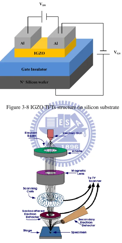
Figure 3-8 IGZO TFTs structure on silicon substrate ... 54
Figure 3-9 Schematic illustration of SEM instrument. ... 54
Figure 3-10 Schematic illustration of TEM instrument. ... 55
Figure 3-11 Schematic illustration of AFM instrument. ... 55
Figure 4-1 SEM image of IGZO thin film without thermal treatment .. 72
Figure 4-2 SEM images of deposited IGZO thin films which are annealed with different temperature in nitrogen ambiance (a) 200°C (b) 300°C (c) 400°C (d) 500°C. ... 72
Figure 4-3 SEM images of deposited IGZO thin films which are annealed with different temperature in oxygen ambiance (a) 200°C (b) 300°C (c) 400°C (d) 500°C. ... 73
x
Figure 4-4 AFM images of deposited IGZO thin films which are annealed with different temperature in nitrogen ambiance (a) control (b) 200°C (c) 300°C (d) 400°C (e) 500°C... 74 Figure 4-5 AFM images of deposited IGZO thin films which are annealed with different temperature in oxygen ambiance (a) 200°C (b) 300°C (c) 400°C (d) 500°C. ... 75 Figure 4-6 XRD patterns of IGZO thin films annealed with different temperature in nitrogen ambiance. ... 76 Figure 4-7 XRD patterns of IGZO thin films annealed with different temperature in oxygen ambiance. ... 76 Figure 4-8 TEM image of IGZO thin films annealed at 500°C. ... 77 Figure 4-9 TEM image indicates a thickness of native oxide. ... 77 Figure 4-10 TEM image indicates a thickness of IGZO thin films about 40 nm and Al2O3 of gate dielectric with thickness about 30.5
nm (IGZO/ Al2O3/ Native oxide/ Si). ... 78
Figure 4-11 XPS analysis of IGZO thin films with annealing temperature 500°C in nitrogen ambiance. ... 80 Figure 4-12 Optical transmittance spectra of IGZO thin films deposited on glass substrate with different annealing temperature in nitrogen ambiance. ... 81 Figure 4-13 Optical transmittance spectra of IGZO thin films deposited on glass substrate with different annealing temperature in oxygen ambiance. ... 82 Figure 4-14 Photograph image of a 500°C annealed IGZO thin film on glass substrate placed on a logo. ... 82
xi
Figure 4-15 IGZO TFTs ID-VG curves with different annealing
temperature in nitrogen ambiance. ... 83 Figure 4-16 IGZO TFTs ID-VG curves with different annealing
temperature in oxygen ambiance. ... 83 Figure 4-17 IGZO TFTs ID-VD curves with different annealing
temperature in nitrogen ambiance (a) no annealed (b) 200°C (c) 300°C (d) 400°C (e) 500°C. ... 85 Figure 4-18 IGZO TFTs ID-VD curves with different annealing
temperature in oxygen ambiance (a) 200°C (b) 300°C (c) 400°C (d) 500°C. ... 87 Figure 4-19 IGZO TFTs ID-VG curves with annealing temperature at
500°C in nitrogen and oxygen ambiance. ... 87 Figure 4-20 C-V characteristics of an Al/HfO2/N+Si capacitor. ... 89
Figure 4-21 C-V characteristics of an Al/Al2O3/N +
Si capacitor. ... 89 Figure 4-22 J-V characteristics of an Al/Al2O3/N+Si capacitor. ... 89
Figure 4-23 IGZO TFTs ID-VG curves with different gate dielectric of
HfO2 and Al2O3... 90
Figure 4-24 IGZO TFTs ID-VD curves with HfO2 as gate dielectric. ... 90
Figure 4-25 IGZO TFTs ID-VD curves with Al2O3 as gate dielectric. ... 91
Figure 4-26 IGZO TFTs ID-VG, IG-VG and ID 1/2
-VG curves with Al2O3 as
1
Chapter 1
Introduction
1.1 Forward
Recently, the display technologies have become an important industry in Taiwan. The products of display technologies include PC monitors,TV screens,notebooks,and cell phones in people daily life. The history of the TFT began with the work of P.K. Weimer at RCA laboratories in 1962. He used thin films of polycrystalline cadmium sulfide (Cds) as the active layer, silicon oxide (SiO2) and gold (Au) as the
insulator and electrodes. Now amorphous silicon (a-Si:H) and polycrystalline Si are used widely as the active layer of thin film transistors (TFT) for the drivers of Active Matrix Liquid-Crystal Display (AMLCD), which integrates TFT-LCD and backlight source module. Recently, the Active Matrix Organic Light Emitting Diode (AMOLED) has been the leading role of display technologies due to the thinner screens and wide angle of view.
But the issue of the material based on a-Si:H as active layer in TFT is low field effect mobility (~1 ) [1], photo sensitivity (low
band gap about 1.7eV) and rather high deposition temperature (~400°C) [2, 3]. Because of the low band gap of a-Si, the photo excited carriers (photo current effect) might make the array of AMLCD and AMOLED out of control in visible region. For the reason, the opaque metals to keep
2
a-Si based channel blind from visible light are integrated necessarily. This causes lower opening of AMLCD pixels and more complicated device fabrication.
Organic light emitting diodes (OLED) has been investigation and important target on the next generation of display technologies. The OLED of display technology is demonstrated to promising for providing power efficient, lightweight and high brightness performance at reasonable voltage and current levels. Because OLED can be lighted by itself, the AMOLED does not need backlight source module. But we need to solve the problem that driving OLEDs need higher voltage and driving current than LCDs for controlling circuit. However, it seems difficult that the a-Si based material low mobility limited on driving circuit.
1.2 Amorphous oxide semiconductors (AOS)
Amorphous oxide semiconductors (AOS) are the materials of high performance, low temperature fabrication even at room temperature (RT) that be used reasonably in flexible electronics. However AOS materials have unstable carriers that generated from oxygen vacancy. Consequently, the deposition process of oxygen pressure will determine the carrier concentration of AOS. So it is important to design and investigation a suitable material and control the oxygen pressure for both properties of large mobility and stable controllability carrier concentration in particular application.
Due to the intrinsic chemical bonding nature that the mobility of a-Si:H (~1 ) is much lower than single crystalline Si
3
(~200 ). The average carrier transportation paths in covalent semiconductors, such as a-Si:H consist of strongly directive sp3 orbitals. The bond angle alter fluctuation significantly the electronic levels that influence high density of deep tail-states as show in figure 1-1.
By contrast, transparent oxide constituting of heavy post transition metal ions with the (n-1)d10ns0 electron configuration where n ≥ 5 are the transparent AOS candidates having high mobility comparable to those of the corresponding crystals. The electron pathway in oxide semiconductor is primarily composed of spatially spread ns orbitals with an isotropic shape as show in figure 1-1. The direct overlap among the neighboring ns orbitals is possible. The degree of overlap of the ns orbitals is insusceptible to the distorted metal-oxygen-metal bonding. The feature shows why the Hall mobility of AOS is similar to the corresponding crystalline phase even the thin films deposit at room temperature.
1.3 Transparent oxide semiconductors (TOS)
Currently, transparent oxide semiconductors (TOS) have attracted keen attention on applications of thin film transistors (TFT) for active layer in display, mobile electronics, optoelectronics, and military
technologies [5,6]. Among of these TOS, amorphous
indium-gallium-oxide (a-IGZO) TFTs [7-13] present promising alternative to a-Si TFTs, poly-Si TFTs and ZnO TFTs. There are many advantageous property of a-IGZO TFTs which high transparency, high field effect mobility, including the capability of large-area and uniform deposition at low temperature, such as room temperature for the
4
fabrication of flexible displays and computers on various substrates, such as glass, plastic and paper. Therefor the a-IGZO is the ideal material for active layer in TFTs which can achieve the purpose of efficient power consumption, low temperature deposition, high transparency, and well driving ability.
1.4 Motivation
The high filed effect mobility and transparent thin films of a-IGZO can be fabricated at low temperature on several substrates by variety of physical and chemical method, such as DC/ or RF magnetron sputtering [14, 15], pulse laser deposition (PLD) [16], molecular beam epitaxy (MBE) [17], sol gel [18, 19], chemical spray pyrolysis [20-23], ink-jet printing [24, 25], chemical bath, and atmospheric pressure plasma jet (APPJ).
In the above mentioned deposition methods, we determinate the APPJ system to deposit a-IGZO thin films because the deposition way has a lot of merits, such as it could be manufacture in the air ambient, economical, easy-to-handle, large area deposition feasibility and controlled quality [26, 27].
The high quality thin films can be deposited in the atmosphere ambient by APPJ, but can’t use the PECVD based on the plasma used methods [28]. And deposit thin films by other plasma CVD processes also in low pressure conditions. The APPJ system is mainly used in high temperature arc plasma, for example, the plasma jet used for diamond synthesis [29] and the inductively coupled plasma (ICP) flash evaporation
5
process for producing ferrite films formation [30] is possible to generate atmospheric pressure cold glow plasma. The atmospheric pressure cold glow plasma which is used the nitrogen gas as a plasma gas, employed a high frequency power source over one kilohertz, and stetted an insulating between two electrodes [31].
Therefore, the APPJ would be quite advantageous than other plasma enhanced CVD from the viewpoint of process cost, and particularly in the application of thin films deposition on ready prepare glass substrates. Numerous films were fabricates by the APPJ system, such as SiOx films
[32], TiOx films [33], ZnO films and Transparent Conductive Oxide
(TCO). Consequently, we can mix two or more solutions that choose appropriate source material to be the precursor of deposition films for an APPJ system that it would be a convenient process for fabrication a variety of thin films, even though a-IGZO thin films.
In recent years, many researchers have been extensively studied targeting for transparent TFTs for the next display generation. Nowadays, various materials have been investigated as candidates of the channel semiconductors, such as hydrogenated amorphous silicon (a-Si:H) [34-36], polysilicon, organic semiconductor [37-41], metal-oxide semiconductors such as zinc oxide (ZnO) [42-47], and so on. The material of ZnO for channel TFT has attracted much attention with its notable advantages over the other semiconductors including high field effect mobility, wide bend gap of 3.37 eV, high transparency in the visible range, and good thermal stability. But the ZnO films examined are polycrystalline [48] even if formed at room temperature. These channels
6
have grain boundaries that deteriorate the TFT performance, stability, and uniformity of the TFT characteristics. However the a-IGZO films also has the similar properties to ZnO films and it can be formed amorphous at room temperature that has better stability and uniformity of TFT characteristics than ZnO TFT.
For the indium-gallium-zinc-oxide ternary system, the IGZO films ratio of indium, gallium, and zinc are very important to determinate the carrier concentration and mobility. The carrier concentration of IGZO is primary determined by the incorporation of cations with large ionic valance such as indium and zinc that are effective to control the carrier concentration due to their strong metal-oxygen bonds. Besides the mobility of IGZO is determined by the indium content fraction because only In3+ meets the electron configuration criterion (n-1)d10ns0(n ≥ 5) of heavy post transition metal cation for ionic AOS among the three cations [49]. In the other hand the gallium ions can effectively suppress the formation of oxygen vacancy and this reduce the carrier concentration in the film owing to the fact that gallium ion forms a stronger chemical bond with oxygen than zinc and indium ions [50]. Figure 1-2 shows the carrier concentration and electron mobility that evaluated by the Hall effect measurement for amorphous thin films deposition by PLD.
The continuous decrease of the thickness of gate oxides used in modern electronics has to confront the limit of material itself. In order to make a breakthrough on what is aforementioned, it is necessary to increase the physical thickness as well as the dielectric constant of the gate dielectrics. Unfortunately, most popular transparent TFT structure
7
employing SiO2 as dielectric material that has low dielectric constant (k)
resulting in low channel modulation effect. Therefore SiO2-based
structures should require higher driving voltage to achieve the same operating efficiency than the other structures incorporating high-k dielectrics. Moreover, in order to have the equivalent insulation efficiency, SiO2 dielectric layer should be thicker than high-k materials.
However, it has a critical drawback, high charge trap density mainly being concentrated into the interfaces between gate electrode and gate insulator, as well as gate insulator and channel layer [52, 53].
In this dissertation, for the purpose of high mobility, optical transparency, stability, wide band gap, room temperature process, and good uniformity over large area, we choose the IGZO thin film for TFTs active layer. Then, we prepared the precursor solution for IGZO film to blend the molarity ratio by dissolving indium, gallium, and zinc nitrate-based that was deposited by APPJ system. Because of the kind of APPJ does not require a complicated vacuum system which would reduce the cost of processing and enlarge the size limit [54]. Moreover, the deposition process is at low temperature which reducing the thermal damage of substrate and make sure the amorphous state of thin film of IGZO. After the thin film deposition, we discuss the influence of TFTs electric characteristic by different post annealing temperature. In the end, for lower driving voltage, lower leakage current, and higher capacitance we are going to substitute high-k material for SiO2 in the TFTs of gate
dielectric. We explore high-k dielectric materials to find that HfO2 and
8
high dielectric constant, relatively low leakage current, low synthesis temperature, wide band gap sufficient to yield a positive band offset with respect to IGZO, and high transparency in visible range [55, 56].
9
Figure 1-1 Schematic orbital drawing of electron pathway (conduction band bottom) in conventional silicon-base semiconductor and ionic oxide semiconductor [4].
Figure 1-2 Room temperature Hall mobility and carrier concentration as function of chemical composition. Values outside and inside parentheses show Hall mobility in and carrier concentration in 1018 cm-3, respectively [51].
10
Chapter 2
Literature Reviews
2.1 Reviews of thin film transistors applications 2.1.1 Thin film transistors
The structure and operation of thin film transistors (TFT) are similar to metal-oxide-semiconductor field-effect transistors (MOSFETs) which are widely used in single crystal silicon applications such as memory cells and microprocessors. TFTs are three terminal devices like the MOSFETs with a source terminal for injecting carriers, a drain terminal for extracting carriers, and a gate terminal for modulating the conductivity of channel. They are fabricated by subsequent deposition of conducting, insulating, and semiconducting thin films onto an insulating substrate. There have many advantages to use an insulating substrate, such as glass or plastic compared to using a semiconductor substrate. First is the substantially lower material cost and second is the insulating material inherently eliminates problems such as parasitic capacitances and latch-up which are either unavoidable or require additional isolation when using a semiconducting substrate [57]. Finally, since the semiconducting layer where the conducting channel is induced during device operation, is deposited onto rather than built into the substrate, there is more freedom in the way in which the device can be structured.
11
which common material is silicon. The characteristics of silicon based TFT depend on the crystalline state. The semiconductor layer can be either amorphous silicon, microcrystalline silicon, or it can be annealed into polysilicon. There are some materials have been used as semiconductors in TFTs include compound semiconductors such as cadmium selenide, metal oxides such as zinc oxide, and organic materials such as pentacene (referred to as an Organic TFT or OTFT), TFTs have also been made using AOS such as a-IGZO.
There are two main structures of TFTs which are shown in figure 2-1. The structure A and B are respectively top gate and bottom gate structure. We determine one of two structures in TFT fabrication by practical requirements and issues. The structure A of top gate has been used in normal field effect transistors for many years but it does not adapt to majority of TFTs fabrications.
The issue is that we must consider the process of dielectric layer deposited would influence semiconductor active layer by thermal treatment or other damage condition. Defects and interface charges would appear in active layer and the interface between dielectric layer and active layer. Therefore, the top gate structure of TFTs electrical properties become worse by defects and interface charges.
Hence, the most of advanced TFTs fabrication adopt bottom gate structure for better quality of semiconductor active layer than top gate structure because the active layer is deposited after gate dielectric layer. To use the bottom gate structure can avoid thermal treatment injuring active layer and also can fabricate devices on silicon substrate as gate
12
electrodes. Then the gate leakage would deal light influence to devices when we use thermal oxide to be gate insulator. But a problem of bottom gate structure we need to solve that is the stability of devices after active layer directly exposed to the air a long time. The reliability of devices became worse because the mists and particles would invade active layer. In this way, there is an effective method to solve this problem that is depositing preservation layer on active layer such as silicon nitride. Then, it can avoid mists and particles invading active layer. But the method would increase the prime cost and influence the active layer by deposition of preservation layer.
2.1.2 TFT as OLED drivers
Passive matrix organic light emitting diode (PMOLED) is a display technology as shown in figure 2-2 (a) [58-59]. The OLED present a specific type of display technology which does not require backlight. An OLED is driven by one data line and one scan line at one time order. Only one scan line would be grounded and other scan lines connect to broken circuit at one time order. The below scan line would be grounded at next time order. This is ordered from first scan line to last scan line and repeat time and again. It would be driven by data lines when one scan line became grounding and the OLEDs connected as shown in figure 2-2 (b) [60].
The main mechanism of PMOLED is persistence of vision to form images to our eyes because OLEDs keep radiating only during one time order. We need to drive OLEDs by large current and high voltage to
13
make them radiating more light for keeping ideal persistence of vision when monitors size became larger. But this movement would make OLEDs having short lifetime and large power consumption. So it is necessary to find out a method to keep OLEDs radiating before scan line connected to grounding and accepting data line at next time.
Active-matrix OLED (Active-matrix organic light-emitting diode) is a display technology for use in mobile devices and televisions. And Active-Matrix refers to the technology behind the addressing of pixels. AMOLED technology continues to make progress toward low-power, low-cost, and large size (e.g. 40-inch) for applications such as TV. An active-matrix OLED (AMOLED) display consists of OLED pixels that have been deposited or integrated onto a thin film transistor (TFT) array to form a matrix of pixels that generate light upon electrical activation as shown in figure 2-3 (a), which functions as a series of switches to control the current flowing to each of the pixels as shown in figure 2-3 (b).
Typically, this continuous current flow is controlled by at least two TFTs at each pixel, one to start and stop the charging of a storage capacitor and the second to provide a voltage source at the level needed to create a constant current to the pixel and eliminating need for the very high currents required for passive OLED matrix operation. Active-matrix OLED displays provide higher refresh rate than their passive-matrix OLED counterparts and they consume significantly less power. Because of this advantage, active-matrix OLEDs well suited for portable electronics, where power consumption is critical to battery life. The amount of power the display consumes varies significantly depending on
14
the color and brightness shown.
2.2 Thin-Film Transistor Operation
It is helpful to first examine the metal-insulator-semiconductor stack in three different conditions: zero, negative, and positive applied gate biases for understand the operation of a TFT. Under these three conditions, figure 2-4 illustrates the band bending in an unipolar n-type semiconductor and the relative shift of the metal Fermi level compared to the semiconductor Fermi level. The system is in equilibrium or a flat-band state and ideally there is no impact on the carrier concentration at the semiconductor-insulator interface with no applied bias, as depicted in figure 2-4 (a). These delocalized majority carrier electrons in the semiconductor are repelled and there is a depletion of majority carriers at the semiconductor-insulator interface when a negative bias is applied to the gate, as depicted by the positive curvature of bands in figure 2-4 (b). However, these delocalized electrons are attracted towards the interface and this creates an accumulation layer of free majority carriers when a positive bias is applied to the gate as shown in figure 2-4 (c). It is accumulation layer that is referred to as the induced channel in a TFT and it is what allows for conduction between source and drain terminals.
So as to induce a channel, and the source and drain terminals are now also considered if the gate is positively biased, current flow along the channel can be achieved by applying a positive voltage to the drain to extract electrons in the channel while keeping the source grounded. According to the square-law model of TFT behavior [61], the drain
15
current ID is in the pre-saturation regime when the applied drain voltage
VDS is less than the pinch-off voltage (VDSAT) and is described as
*( ) + (2-1)
Where CG is the gate capacitance, the turn-on voltage VON is defined as
the smallest applied gate voltage that causes a non-negligible increase in drain current for a given drain voltage, W and L are the TFT’s width and length, and μ is the mobility.
The drain current ideally becomes independent of the drain voltage as the drain voltage increases and exceeds , and is said to be in saturation regime where ID is given by
( ) (2-2)
The TFT is said to be operating in the cutoff state if or if
is negative and according to the simplistic square-law model, it is
assumed that . These three equations for ID and VDSAT constitute
the square-law model and allow the drain current to be modeled for any given combination of drain and gate voltages.
Thin film transistors are also classified by sign of VON. There are no
current flows when the gate voltage bias is zero applied, if VON is positive
for an n-channel TFT (i.e. the device is normally off) and the device is referred to as an enhancement mode device. There is a sufficiently high carrier concentration in the channel that even with no applied bias to the
16
gate if VON is negative, conduction between the source and drain can
occur (i.e. the device is normally on). In this case, negative gate voltage is required to turn the TFT off and the transistor is referred to as a depletion mode device. Enhancement mode TFTs are generally preferred in circuit applications because of their normally off nature and lower power consumption, but depletion mode devices can be useful in certain circuit applications, e.g. as active loads.
2.3 Deposition methods of IGZO films
The methods of deposition IGZO films have distinct classification. In this paper, we categorize them in physical and chemical type that representing the source of films is solid and liquid. Following the exposition will discuss them in detail.
2.3.1 Magnetron sputtering
The sputtering method is working in the glow discharging region which has higher energy and density of electrons. To put the substrate at anode and set the targets at cathode in the argon ambient, then the cations which accelerated by the electrical field bombard the target. At this time, the targets of atoms are leaved out and going to the substrate to form the IGZO films. The reason of the cations which is driving to target is the potential of plasma always higher than chamber, target and substrate. Moreover, target connect with cathode will increase the potential difference between plasma and target. If setting a magnet under the target, there was an external magnetic field to increase the plasma density, so the
17
cations which bombard the target will increase simultaneously. It is difficult to discharge with the DC power when the low conductivity materials or insulators were to be the deposition substrate. So, there have to use the RF power which the frequency needs to reach the grade of megahertz (usually 13.56MHz) to be the power supply. Using the self-bias phenomenon in the RF discharge, it can make the target potential will always in negative values to ensure the bombardment will almost continuously which is same capability as the DC discharge.
So far, the sputtering technique is one of the most common in deposition the IGZO films, including electrodes of flat display and energy efficiency windows. The generally properties of sputtering are described following:
(1) Widely scope of the process films such as metal, alloy and insulator.
(2) The films thickness can control by the apply power and process times.
(3) The stable, uniform and large area films can be obtained.
(4) Because of higher bombardment energy, so it can deposit the excellent adhesion and crystallization films.
(5) Long target lifetime, so it can operate at continuous and automatic long time process.
There is another magnetron sputtering method which getting high density plasma by RF-DC couple manner. In general RF magnetron sputtering, the self-bias of the target can change with the RF frequency and power, and it controls the ion energy of bombarding to the target.
18
When the RF frequency increased, the self-bias of the target will decreased, the RF power increased, the self-bias of the target will also increase. However, in the RF-DC couple magnetron sputtering system, the RF power is mainly to generate high density plasma, and the DC power is to adjust the electric potential of the target, by doing that is easy to control the deposition conditions.
2.3.2 Pulsed laser deposition
Pulsed laser deposition (PLD) is a technology where a high energy density focusing pulsed laser beam is struck a target of the material that is to be deposited. The target is vaporized which deposits it as a thin film on substrate. This method can be applied on many materials, so it can deposit lots of thin films. But the growth rate of PLD is extremely slow; therefore, it is not a mass production technology. This process can occur in ultra-high vacuum or in the presence of a ambient gas, such as oxygen which is commonly used when depositing oxide to fully oxygenate the deposited films.
The PLD basic machinery is simple relative to many other deposition techniques, the physical phenomena between laser and target interaction and the film growth are quite complex. The absorption energy is converted to electronic excitation and thermal energy resulting in evaporation and plasma formation when the laser pulse is absorbed by the target. The ejected varieties full of the surrounding vacuum including atoms, molecules, electrons, ions, clusters, particulates and molten globules, before depositing on the typically hot substrate.
19
There are a number of advantages of PLD over other thin film deposition methods, these include:
(1) The most advantage is that it is versatile. This method can be applied on many thin films including metal, oxides, semiconductors and even polymer. It is unlike Molecular beam epitaxy (MBE) and Chemical vapor deposition (CVD), where different source of precursors are required for each element of the desired compound.
(2) It can be maintained the target composition in the deposited thin films. Because of the very short duration and high energy of the laser pulse, target material immediately toward the substrate, every component of the phase has an analogous deposition rate, so the thin films composition is almost unchanged.
(3) The energy associated with the high ionic content in laser ablation plumes and high particle velocities appear to aid crystal growth and lower the substrate temperature required for epitaxy.
(4) PLD is clean, low cost and capable of producing simply by switching several different targets.
There are also a heaps of advantages of PLD, these include:
(1) PLD brings difficulty to controlling thickness uniformity across the sample, but this problem can be overcome, to some extent, by scanning the laser beam on a larger size target.
(2) The plume of ablated material is highly forward directed, which causes poor conformal step coverage. It also makes thickness monitoring difficult.
20
(3) There is an intrinsic splashing associated with laser ablation itself, which produces droplets or big particles of the target material on the substrate surface. This is particularly serious as it will result in device failure from an industrial perspective.
2.3.3 Spray pyrolysis
Deposition IGZO thin films by spray pyrolysis has been used for a long time. The deposition material can use solid or liquid source, according to the previous statement of the definition of the deposition method, it may be categorized to the physical type, but it is similar to the CVD method, so we still categorizing it in chemical manner.
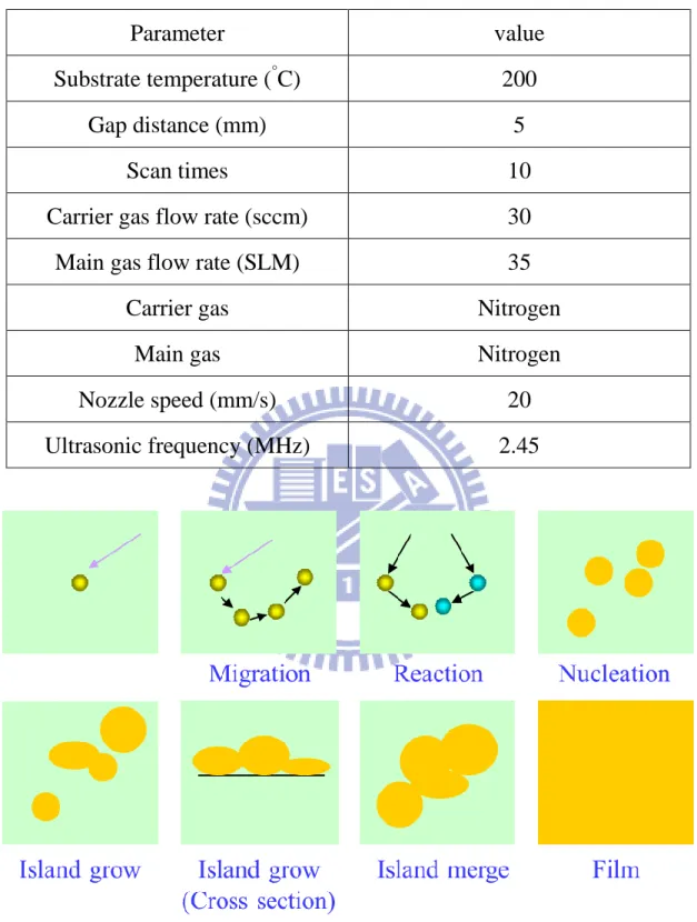
Spray pyrolysis is the most in common uses in the pyrolysis manners. The precursor solution is pulverized as affine mist via a spray nozzle and a carrier gas at high pressure in spray pyrolysis. The so produced mist condenses on a preheated substrate, and is instantly pyrolysed (spray pyrolysis). The process can be conducted in one or more pulses to obtain uniform films. Spray pyrolysis is suitable for substrate with complex geometry, and can be used for a variety of oxide materials. Although the first impression of spray pyrolysis is simple to do, but is concerns at least seven parameters, including heater temperature, carrier gas flow rate, gap distance, solution drop size, solution component, solution flow rate and substrate velocity through the heater.
There is different reaction with increasing the substrate temperature when the solution drops leave from nozzle to the substrate. From figure 2-7, in process A, the solution drop sprinkled on the substrate, vaporizes,
21
then leaves a dry precipitate in which decomposition occurs; in process B, the solvent evaporates before the solution drop arrives at the surface and the precipitate bombards upon the surface where decomposition occurs; in process C, the solvent vaporizes as the solution drop accesses the substrate, then the solid melts and vaporizes, its vapor diffuses to the substrate to undergo a heterogeneous reaction there; in process D, at the hugest temperatures, the metallic compound vaporizes before it arrives the substrate and the chemical reaction takes place in the vapor phase. Apparently, we hope not to happen to the process A and D, because it will cause rough and viscosity thin films. So, select the appropriate substrate temperature and make the uniform and equal size of droplet will help the reaction perfectly.
The advantages of spray pyrolysis are summarized below: (1) The spray pyrolysis can be easy and cheap.
(2) Substrate with complex geometries can be coated. (3) Leads to uniform and high quality coatings.
(4) Low crystallization temperatures. (5) Porosity can be easily tailored. 2.3.4 Sol gel coating
The sol-gel coating method is a chemical solution deposition in atmospheric pressure and a wet-chemical technique widely used in the fields of materials science and ceramic engineering. Such methods are used primarily for the fabrication of materials (typically a metal oxide) starting from a chemical solution which acts as the precursor for an
22
integrated network of either discrete particles or network polymers. Typical precursors are metal alkoxides and metal chlorides, which undergo various forms of hydrolysis and poly-condensation reactions. In the chemical procedure, the sol (or solution) gradually evolves towards the formation of a gel-like diphasic system containing both a liquid phase and solid phase whose morphologies range from discrete particles to continuous polymer networks. In the case of the colloid, the volume fraction of particles (or particle density) may be so low that a significant amount of fluid may need to be removed initially for the gel-like properties to be recognized. This can be accomplished in any number of ways. The simplest method is to allow time for sedimentation to occur, and then pour off the remaining liquid. Centrifugation can also be used to accelerate the process of phase separation.
Removal of the remaining liquid (solvent) phase requires a drying process, which is typically accompanied by a significant amount of shrinkage and densification. The rate which the solvent can be removed is ultimately determined by the distribution of porosity in the gel. The ultimate microstructure of the final component will clearly be strongly influenced by changes imposed upon the structural template during this phase of processing.
Afterwards, it will be necessary that thermal treatment or firing process in order to favor further poly-condensation and enhance mechanical properties and structural stability via final sintering, densification and grain growth. One obvious advantage of using this method as compared to more traditional processing technology is to
23
achieve densification at a much lower temperature.
The precursor sol can be cast into a suitable container with the desired shape or used to synthesize powders to deposit on a substrate to form a film. The sol-gel approach is a low-cost and low-temperature technique that allows the control of the chemical composition of fine products. Even small quantities of dopants, such as organic dyes and rare earth elements, can be introduced in the sol and end up uniformly dispersed in the final product. It can be used in ceramics processing and manufacturing as an investment casting material, or as a means of producing very thin films of metal oxides for various purposes.
2.3.5 Dip coating
Dip coating is a conventional method of deposition thin films for research purpose. Uniform films can be applied onto planar substrate. Spin coating is used more often for industrial processes. The process of dip coating is putted the substrate in the deposition solution first, and then pull up the substrate in regular speed, after that the successful thin film will obtained by drying and annealing. This way of deposition thin film is one of the most common used in sol-gel method.
There are many properties of dip coating manner:
(1) It can be deposited on the irregular surface or double-faced substrate.
(2) Few nanometers of thin films can be acquired. (3) Simple operation, but usually unstable.
24
(5) The edge of substrate will gathered deposition solution to cause non-uniform films.
The dip coating process can be separated into five procedures:
(1) The substrate is immersed in the solution of the coating material at a constant speed.
(2) The substrate has remained inside the solution for a while and is started to been pulled up.
(3) The thin layer deposits itself on the substrate while it is pulled up. The withdrawing is carried out at a constant speed to avoid any vibration. The speed plays an important role to determine the thickness of the coating layer.
(4) Excess fluid will drain from the substrate surface.
(5) The solvent of the fluid will evaporate when forming the thin film. Evaporation starts already during the deposition and drainage steps for volatile solvents, such as alcohols.
2.4 Atmospheric pressure plasma system 2.4.1 Corona discharge
A corona is a process by which a current develops between two high-potential electrodes in air, by ionizing that fluid to create a plasma around one electrode, and by using the ions generated in plasma processes as the charge carriers to the other electrode.
It usually involves two asymmetric electrodes in corona discharge, one highly curved such as the tip of a needle or a narrow wire, and
25
another one of low curvature such as a plate or the ground. For the generation of the plasma, the high curvature assures a high potential gradient around one electrode.
Coronas can be positive or negative. It is calculated by the polarity of the voltage on the high curvature electrode. It will have a positive corona, if the curved electrode is positive associated to the flat electrode, and vice versa. The physics of positive and negative coronas are obviously different. This asymmetry structure is a result of the great difference in mass between electrons and positively charged ions, and so only the electron having the ability to undergo a significant degree of ionizing inelastic collision at common temperature and pressures.
2.4.2 Dielectric barrier discharge (DBD)
Dielectric barrier discharges involve a specific class of high voltage, ac, gaseous discharges that typically operate in the near atmospheric pressure range. Their defining feature is the presence of dielectric layers that make it impossible for charges generated in the gas to reach the conducting electrode surfaces. The voltage applied across the gas exceeds that required for breakdown with each half cycle of the driving oscillate, and the formation of narrow discharge filaments initiates the conduction of electrons toward the more positive electrode. The voltage drop across the filament is reduced until it falls below the discharge sustaining level as charge accumulates on the dielectric layer at the end of each filament, so the discharge is quenched. The low charge mobility on the dielectric not only contributes to this self-arresting of filaments but also limits the
26
lateral region over which the gap voltage is diminished, thereby allowing parallel filaments to form in close proximity to one another. Thus, the entire gas filled space between parallel electrodes can become, on average, uniformly covered by transient discharge filaments, each roughly 0.1mm in diameter and lasting only about 10ns.
The DBD’s has provided the basis for a broad range of applications and fundamental studies, because of the unique combination of non-equilibrium and quasi-continuous behavior. It has generated interest in optimizing conditions for specific chemical reactions in industrial ozone reactors. To this end, experimental DBD studies have explored different gas mixtures, electrical characteristics, and geometries. The related work has focused on maximizing the ultraviolet radiation from excimer molecules produced in DBD’s. Several researchers have designed single filament dynamics in order to account for the many reactions including electrons, ions, neutral atoms, and photons. These efforts have been moderately successful in explaining and predicting the chemical and radiative properties of different DBD systems. On another research effort, it has been seen that the transverse spatial distribution of discharge filaments in 2D, parallel plate DBD’s can take the form of stable, large scale patterns reminiscent of those associated with magnetic domains. These patterns have been modeled with some success using methods that apply generally to pattern formation in nonlinear dynamical systems. Thus, the dynamical interactions between filaments, as well as the chemical and electronic interactions within filaments have proven interesting.
27
2.4.3 Atmospheric pressure plasma jet
Atmospheric pressure plasma jet is meaning that operating at atmospheric pressure and it is non-thermal glow discharge plasma system. The non-thermal plasma generates highly reactive ions, electrons and free radicals. The reactive species are directed onto a surface where the desired chemistry occurs. However the overall gas temperature remains quite cold, but the electrons are quite hot, typically 50-300°C.
2.4.4 Arc plasma
The operation of arc plasma is similar to an arc-welding machine, where an electrical arc is struck between two electrodes. The high energy of arc creates high temperatures ranging from 3000°C to 7000°C. The plasma is highly ionized gas which is enclosed in a chamber. The waste material is fed into the chamber and the intense heat of the plasma break down organic molecules into their elemental atoms. In the strict control of the process, these atoms recombine into harmless gases, such as carbon dioxide. Solids such as glass and metals are melted to form materials, similar to hardened lava, in which toxic metals are encapsulated. There is no burning or incineration and no formation of ash with plasma arc technology. There are two main types of plasma arc processes: plasma arc melter and plasma torch.
Plasma arc melters have very high destruction efficiency. They are very robust; they can treat any waste with minimal or no pretreatment; and they produce a stable waste form. The arc melter uses carbon electrodes to strike an arc in a bath of molten slag. The consumable
28
carbon electrodes are continuously inserted into the chamber, eliminating the need to shut down for electrode replacement or maintenance. The high temperatures produced by the arc convert the organic waste into light organics and primary elements.
Combustible gas is cleaned in the off-gas system and oxidized to CO2 and H2O in ceramic bed oxidizers. Due to the use of electrical
heating in the absence of free oxygen, the potential for air pollution is low. The inorganic portion of the waste is retained in a stable, leach-resistant slag.
In plasma torch systems, an arc is struck between a copper electrode and either a bath of molten slag or another electrode of opposite polarity. Plasma torch systems have very high destruction efficiency with plasma arc systems; they are very robust; and they can treat any waste or medium with minimal or no pre-treatment. The inorganic portion of the waste is retained in a stable, leach-resistant slag. The air pollution control system is larger than for the plasma arc system, due to the need to stabilize torch gas.
29
A
B
Figure 2-1 (a) Top Gate Structure (b) Bottom Gate Structure
(a) (b)
30
(a) (b)
Figure 2-3 (a) AMOLED (b) AMOLED Control Circuit
Figure 2-4. Energy band diagrams for a metal-insulator-semiconductor capacitor, assuming a unipolar n-type semiconductor under three gate bias conditions: (a) no bias, (b) negative bias, and (c) positive bias.
31
Figure 2-5 Schematic illustration of magnetron sputtering [62].
32
Figure 2-7 Description of the deposition process with raising the substrate temperature [64].
.
Figure 2-8 Schematic illustration of equipment for spray pyrolysis deposition [64].
33
Figure 2-9 Sol-gel process
Figure 2-10 Steps of the dip coating process: dipping of the substrate into the coating solution, wet layer formation by withdrawing the substrate and gelation of the layer by solvent evaporation [65].
34
Figure 2-11 Schematic the principle of corona discharge [66].
35
Figure 2-13 Schematic illustration of the AP plasma jet structures [68].
36
Table 2-1 Density of charge species in the plasma discharge [70]
Source Plasma density (cm-3)
Low pressure discharge 108-1013
Arc and plasma torch 1016-1019
Corona discharge 109-1013
Dielectric barrier discharge 1012-1015
37
Chapter 3
Experiments
3.1 Experimental Procedures
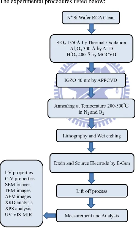
The experimental procedures listed below:
38
3.2 Experimental process step
3.2.1 The structure and gate dielectric of TFTs fabrication
In the Literature Reviews, the fabrication and properties of bottom gate type thin film transistors using IGZO film as active layers will be described. We use the bottom gate structure for TFTs fabrication on N+-type silicon wafer as substrate. When using IGZO thin film as active channel material of TFT, usually adopt bottom gate structure for better quality of semiconductor active layer than top gate structure. Because of the active layer is deposited after gate dielectric layer. It will be avoided the plasma bombarding or thermal treatment damaging active layer when deposited gate dielectric layer. The silicon wafer be used as substrate and gate electrode of the TFTs fabrication, and chose N+-type silicon wafer for lower resistance and bias voltage of gate electrode than N-type silicon wafer.
After RCA clean procedure, we choose three kinds of material for the gate insulator on silicon wafer. We describe it following: First we use silicon dioxide (SiO2) as the gate insulator because it compatible with
silicon wafer. The SiO2 deposited by thermal oxidation in furnace setting
the temperature at 1050°C with 80 minutes. The thickness of SiO2 is
1350Å , and the slightly thick thickness can avoid the gate leakage current to influence device I-V properties. The other materials are Al2O3 and
HfO2 that have higher dielectric constant (k) than silicon dioxide (~3.9).
In order to have the equivalent insulation efficiency, SiO2 dielectric layer
should be thicker than high-k materials. Therefore, we replace SiO2 with
39
reduce the driving voltage to achieve the same operating efficiency compared with SiO2-based structures. In addition, Al2O3 and HfO2 have a
large band gap (~8.8eV and ~5.68eV) sufficient to yield a positive band offset with respect to IZGO. So we respectively deposited Al2O3 300Å on
silicon wafer by Atomic Layer Deposition (ALD) and HfO2 400Å by
Metal-organic Chemical Vapor Deposition (MOCVD). 3.2.2 IGZO thin film deposited by APPJ
First, the precursor solution for IGZO film was prepared by dissolving 0.067M of zinc nitrate hexahydrate [Zn(NO3)2·6H2O], 0.067M indium nitrate hydrate [In(NO3)3·xH2O] and 0.067M gallium nitrate
hydrate [Ga(NO3)3·xH2O] in distilled water. These precursors were mixed
at an atomic ratio of In:Ga:Zn = 1:1:1.
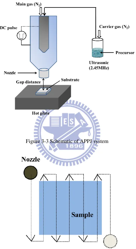
According to our group had been study of APPJ system, we could set a suitable deposition condition including gap distance, substrate temperature, carrier gas flow rate, main gas flow rate, and nozzle speed in APPJ system. When the precursor solution for IGZO was prepared already, the carrier gas carried mists of precursor solution to the plasma region. The carrier gas and mists of precursor solution were mixed with main gas, and these gases would become plasma by arcing mechanism because of high pulsed voltage. Precursor, carrier gas, and main gas would participate with some reactions in plasma region. And then main gas would carry these plasmas to substrate and reduce the plasmas temperature. We could use a computer to control scanning path including starting point and terminal point. The main gas carried plasmas to
40
substrate and the IGZO films were deposited by chemical vapor deposition.
Chemical vapor deposition (CVD) is the process of depositing a solid film on the wafer surface through one or more volatile precursors, which react or decompose on the substrate surface to produce the desired deposit. Frequently, volatile by-products are also produced, which are removed by gas flow through the reaction chamber. The sample surface or its vicinity is heated in order to provide additional energy to the system to drive the reactions. The plasma and radicals would cause reactions and nucleation on samples, and then IGZO films would grow from island shape to continuous films.
3.2.3 Annealing
After IGZO thin films deposited on the wafer covered with insulator by APPJ, we put these samples in furnace. Then, these samples were annealed for 30 min at various temperature in the range from 200 to 500°C in oxygen ambiance. We expect that oxygen atoms can diffuse in the films and repair oxygen vacancies which in the IGZO films. If in the transparent TFT fabrication, it will not suit for annealing in oxygen ambiance, because oxygen will influence the electrode and effect device electrical characteristics. So we also anneal for 30 min in nitrogen ambiance at various temperature in the range from 200 to 500°C, because nitrogen is inert gas.
41
After IGZO deposited, the next step was to define each TFT’s active layer region. This procedure was carried out in lithography area by photo resist spinner and mask aligner. The patterns on mask for defining active layer region, drain electrodes, and source electrodes is shown in figure 3-6. We etched IGZO thin film by 0.5% hydrochloric acid water solution after photo resist had been put cover over IGZO film as a barrier layer for the region which we wanted to reserve.
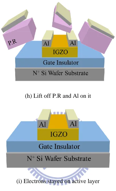
When IGZO film which we did not want to reserve had been etched completely, the next step was to define drain and source electrodes. At the first, we though the procedures of defining drain and source electrodes were depositing aluminum and etching it by lithography and wet etching. But the active layer was under drain and source electrodes. It is difficult to choose suitable acid solution which kept good etching selectivity between aluminum and IGZO. IGZO film would be etched faster than aluminum by any acid solution. Therefore, we use lift-off process to replace etching process to define drain and source electrodes on active layer.
3.2.5 Lift-off process
Lift-off process contains several steps, we first put photo resist as a cover over IGZO region which we did not want aluminum deposited. And then we used E-Gun evaporation to deposit aluminum about 1000Å on silicon wafer. At last, we set silicon wafer in acetone with ultrasonic shaking to lift off aluminum on the photo resist. Then, a part of aluminum would stay on active layer as drain and source electrodes. And the device
42
as shown in figure 3-8 would be measured electrical properties and the results would be discussed in next chapter.
3.3 Characterization analysis equipment 3.3.1 Scanning Electron Microscopy (SEM)
SEM stands for scanning electron microscope. The SEM is a microscope that substitute electron for light to form an image. Scanning electron microscopes have developed new areas of study in the medical and physical science communities since their development in the 1950. SEM uses a focused beam of high energy electrons to generate a variety of signals at the surface of solid samples. The signals that derive from electron and sample interactions reveal information about the sample including external morphology, chemical composition, and crystalline structure and orientation of materials making up the sample. The researchers can inspect a much larger variety of samples by SEM.
Accelerated electrons carry significant amounts of kinetic energy in the SEM. When the incident electrons are decelerated in the solid sample, this energy is dissipated as a variety of signals produced by electron and sample interactions. These signals include secondary electrons, backscattered electrons, diffracted backscattered electrons, photons and heat. Secondary electron and backscattered electrons are commonly used for imaging samples. Secondary electrons are most valuable for showing morphology and topography on samples and backscattered electrons are most valuable for illustrating contrasts in composition in multiphase sample. X-ray generation is produced by inelastic collisions of the
43
incident electrons with electrons in discrete orbital of atoms in the sample. X-rays are fixed wavelength as the excited electrons return to lower energy states. Thus, characteristic X-rays are produced for each element in a mineral that is excited by the electron beam. SEM analysis is considered to be non-destructive; that is, X-rays generated by electron interactions do not lead to volume loss of the sample, so it is possible to analyze the same materials repeatedly.
The SEM has many advantages over traditional microscopes. We describe it following:
(1) It has large depth of field, which allows more of a specimen to be in focus at one time.
(2) SEM has much higher resolution so closely spaced specimens can be magnified much higher levels.
(3) Researcher has more control in the degree of magnification, because of the SEM uses electromagnets rather than lenses.
3.3.2 Transmission electron microscopy (TEM)
Transmission electron microscopy (TEM) is a microscopy technique whereby a beam of electrons is transmitted through an ultra-thin specimen, interaction with the specimen as it passes through. The interaction of the electrons transmitted through the specimen form an image that is magnified and focused onto an imaging device, such as a fluorescent screen, on a layer of photographic film, or to be detected by a sensor such as a charge coupled device (CCD) camera.
44
capable of imaging at a significantly higher resolution than light microscopes. Therefore, the instrument’s user to examine fine detail even as small as a single column of atoms, which is tens of thousands times smaller than the smallest resolvable object in a light microscope. TEM is an important analysis method in the physical and biological sciences fields that application in cancer research, virology, materials science as well as pollution, nanotechnology, and semiconductor research.
At smaller magnifications TEM image contrast is due to absorption of electrons in the material, due to the thickness and composition of the material. At higher magnifications complex wave interactions modulate the intensity of the image, requiring expert analysis of observed images. Alternate modes of use allow for the TEM to observe modulations in chemical identity, crystal orientation, electronic structure and sample induced electron phase shift as well as the regular absorption based imaging.
3.3.3 Atomic Force Microscopy (AFM)
Atomic force microscopy is a manner of measuring surface morphology on a scale from angstroms to 100 microns. The technique involves imaging a sample through the use of a probe or tip, with a radius of 20 nm. The tip is held several nanometers above the surface using a feedback mechanism that measures surface tip interactions. Variations in tip height are recorded while the tip is scanned repeatedly across the sample, producing a topographic image of the surface.
![Figure 2-7 Description of the deposition process with raising the substrate temperature [64]](https://thumb-ap.123doks.com/thumbv2/9libinfo/8600706.190116/45.892.241.648.112.335/figure-description-deposition-process-raising-substrate-temperature.webp)