國
立
交
通
大
學
電子工程學系 電子研究所碩士班
碩
士
論
文
新式雙閘極複晶矽奈米線薄膜電晶體與記憶體元件
A Novel Double-Gated Poly-Si Nanowire Thin Film
Transistor and SONOS Memory
研 究 生:張育嘉
指導教授:林鴻志 教授
黃調元 教授
新式雙閘極複晶矽奈米線薄膜電晶體與記憶體元件
A Novel Double-Gated Poly-Si Nanowire
Thin-Film-Transistor and SONOS Memory
研 究 生:張育嘉 Student:Yu-Chia Chang 指導教授:林鴻志 博士 Advisors:Dr. Horng-Chih Lin 黃調元 博士 Dr. Tiao-Yuan Huang
國 立 交 通 大 學
電子工程學系 電子研究所碩士班
碩 士 論 文
A Thesis
Submitted to Department of Electronics Engineering & Institute of Electronics College of Electrical and Computer Engineering
National Chiao-Tung University in Partial Fulfillment of the Requirements
for the Degree of Master in
Electronic Engineering June 2009
Hsinchu, Taiwan, Republic of China
新式雙閘極複晶矽奈米線薄膜電晶體與記憶體元件
研 究 生:張育嘉 指導教授:林鴻志 博士 黃調元 博士
國 立 交 通 大 學
電子工程學系 電子研究所碩士班
摘 要
在本篇研究論文中,我們構思並成功地驗證一種簡易且具經濟效益的製作流 程。此技術無需借助昂貴的微影設備與製程,即可製作出新式奈米線通道的薄膜 電晶體。此技術運用一獨特的二階段乾式蝕刻技巧,可在一閘電極的兩側形成奈 米極尺寸孔洞,並在沉積一矽膜將其填滿後,利用異向性蝕刻,自我對準地形成 奈米線通道。運用此流程,可完成具有獨立雙閘極奈米線電晶體結構,在電性分 析上可賦予更有彈性的操作模式,也可讓吾人針對各種操作模式進行比較與分 析。我們也加入二氧化矽-氮化矽-二氧化矽(ONO)堆疊薄膜作為閘極介電層,及 利用原生摻雜複晶矽作為源極/汲極(in situ doped source/drain)的技巧,可以有效 提升閘極控制能力並且改善元件特性。基於此結構製作的記憶體元件,其特性上 在具有更多彈性的雙閘極操作下,可提升元件基本電性及寫入/抹除速度。A Novel Double-Gated Poly-Si Nanowire Thin Film
Transistor and SONOS Memory
Student:Yu-Chia Chang
Advisors:Dr. Horng-Chih Lin Dr. Tiao-Yuan Huang
Department of Electronics Engineering and Institute of Electronics National Chiao Tung University, Hsinchu, Taiwan
ABSTRACT
In this thesis, a simple and cost-effective method for fabricating poly-Si nanowire (NW) thin film transistor (TFT) without the necessity of advanced lithography tools is proposed and demonstrated. In this scheme, a unique two-step etching is developed to form nano cavities at the sidewalls of an electrode. After filling the cavities with a Si film, an anisotropic etch is subsequently performed to define the NW structures in a self-aligned manner. With the proposed scheme, independent double-gated NW devices could be constructed. With such configuration, more flexibility in device operation could be provided. Characteristics of different operation mode are compared and analyzed. With the implementation of oxide-nitride-oxide (ONO) gate dielectrics and in-situ doped source/drain (S/D), dramatic improvements in device characteristics can be achieved. Based on the proposed scheme, NW TFT-SONOS memory devices were also fabricated and characterized. The two independent gates are shown to increase the
Acknowledgement
寫到了這章節代表著我的論文已完成 99%了... 還記得在 group meeting 上第一次生澀的自我介紹『老師各位學長姐大 家好,我叫張育嘉,大家都叫我阿嘎。大學念交大材料,喜歡看日劇,請 多多指教!』原來從那天開始我喜歡上了 ADTL,哪怕是大伙一起夜唱一 起實驗室出遊一起考試一起爆肝作實驗搶時段一起實驗室搬家一起合 購,只要和大家在一起每天都是愉快的。 當然這都要感謝實驗室的頭兒黃調元教授及林鴻志教授,謝謝你們的 指導。不管在研究上的態度或是生活中的待人處世,真的,在你們身上挖 到了不少寶。對你們的感謝不是三言兩語可以說盡的,謝謝你們當初可以 讓我進入這樣棒的實驗室。 接著,給實驗室的學長群、同學及學弟妹們。林哲民、徐博、蔡子儀、 大師謝謝你們。大師,沒有你在旁的帶領我想我實驗無法這樣順利。徐博, 謝謝你即使和你在五四三時也能得到許多啟發。蔡子儀,謝謝你總是會有 便宜又大碗的好東西。林哲民學長,謝謝你讓我知道業界一些事好讓我有 個心理準備。君帆、瑄勻、馬卡、林政毛、張祐寧、政建、gaygay、桀桀、 施維濤。君帆,感謝妳總是在我身邊當一位最稱職的聆聽者,要幸福唷。 馬卡、林政毛,博班之路加油。張祐寧,你讓我看見作研究的應有的精神。 政建,下次去澳門玩時一定請你當地陪。Gaygay,感謝你總是當起實驗室 的活動負責人實驗室感情的幕後推手。桀桀,隨時可以打瞌睡這點讓我不 得不佩服你。施維濤,你那跳 tone 的思維總是會讓人會心一笑。 還有小碩一們也謝謝你們展現了青春活力。另外還有已經畢業和我生日只 差一天的 David,謝謝你即使畢業了還是這樣熱心的幫助我,真的很謝謝 啦! 材料所的同學薇蓁、怡萱、張文星、許鋪哈。你們總是在一旁給我鼓 勵和你們在一起特別會人來瘋,能認識你們真好,你們也要加油。也給認 識了快十年的珮芸,你總是會是那在我遇到低潮支持我繼續下去的力量, 謝謝妳。還有也同樣認識十年看我長大的 my lovely E.T.,從我高中畢業後 便只能寒暑假和你見面了,雖然一期一會但是妳也總是特別關心著我! 你,該怎麼說呢?對我來說你真的很特別,很多話想對你說但是沒說出 口不過我想你一定了解的,謝謝你。 最後也要給我的家人,爸爸、媽媽謝謝你們給我的一個無憂無慮而且 溫暖的家讓我可以任性的做我自己想做的事。謝謝老姐、老哥,長大了才 發現原來我們的感情如此深厚。謝謝未來的嫂嫂,你總是這樣的關心我給 我最大的支持。謝謝猪大王,你總是利用你的天真讓我忘記生活中不愉快。CONTENTS
Abstract……….………...…..………….…I Acknowledgement……….………...……….…………...Ⅲ Contents……….………..………...……....Ⅳ Table Captions………….………...Ⅵ List of Figure Captions………,...Ⅶ
CHAPTER 1 Introduction
1-1 Overview of Multiple-Gated Structure and Nanowire Technology.……..…..1 1-2 Overview of Nonvolatile Memory………..………... 3 1-3 Motivation of this Study...………5 1-4 Organization of the Thesis………...6
CHAPTER 2 Device Structure, Fabrication, and Measurement Schemes 2-1 Structure and Fabrication of Embedded Poly-Si Nanowire TFT Devices…...7
2-2 Fabrication of NWTFT- SONOS Memory Devices………...10 2-3 The Measurement Setup……….11
CHAPTER 3 Effects of Operational Modes, Gate Dielectric Materials, and Source/Drain Doping Processes on Device Characteristics
3-1 Characteristics of NW Devices with Implanted Source/drain……..……….13 3-2 Effects of ONO Gate Dielectric on Device Characteristics…………...15 3-3 Effects of in situ Doped Source/Drain on Device Characteristics…...17
CHAPTER 4 Characteristics of Nanowire TFT-SONOS Memory 4-1 Program/Erase Operation Principles and Characteristics………..…19 4-2 Reliability Characteristics and Issues………...22 4-3 Effects of NW Channel Thickness………...24
CHAPTER 5 Conclusions and Future Work
5-2 Future Work...27
References………...29
Figures………...36
TABLE CAPTIONS
CHAPTER 2
Table 2-1 Summary of the conditions of the three operation modes.…….…..…….40
CHAPTER 3
Table 3-1 Summary of the two types of devices with different gate dielectrics.
Type-A devices have silicon dioxide as gate dielectrics, while Type-B
FIGURE CAPTIONS
CHAPTER 2
Fig. 2-1 Fig. 2-1 (a) The layout and (b) Cross-sectional view of embedded
NWTFT……….………..………….36
Fig. 2-2 (a) Deposition of gate stack layer. (b) Definition of 1st gate(c) Lateral etching (d) SPC (e) S/D ion implantation. (e-1-1) Etching poly-Si. (e-1-2) Deposition of in situ doped poly. (f) Definition of S/D and formation of NW channel. (implanted S/D type). (f-1) Definition of S/D and formation of NW channel. (in situ doped S/D type). (g) Deposition of 2nd gate oxide and formation of 2nd gate………..………..36 Fig. 2-3 Cross-sectional TEM image of embedded NW TFT and NW channel profile
along line AB of the layout.………...….39 Fig. 2-4 (a) NWTFT-SONOS memory with the ONO storge layer near 1st gate. (b)
NWTFT-SONOS memory with the ONO storge layer near 2nd gate……...40 Fig. 2-5 Cross-sectional TEM image of the NWTFT-SONOS memory device and
NW channel profile along line AB of the layout.………...41
CHAPTER 3
along the C–D lines shown in (a). Projection of the second gate (shaped by the dashed lines) is also shown. From the figure, it can be seen that ungated regions (indicated by the double-head arrows) exist between the inner conduction channel (gated by the first gate) and S/D………..43
Fig. 3-3 (a) Vth and (b) subthreshold swing of the NW devices under various
operation modes as a function of the channel length………...44
Fig. 3-4 Output characteristics of an NW TFT under various operation mod…...…45
Fig. 3-5 Comparisons of output drain current of DG mode with the sum of SG-1 and SG-2 modes………..………45
Fig. 3-6 Transfer characteristics of an NW device with ONO dielectrics and implanted S/D.………..………46
Fig. 3-7 Transfer characteristics of a device with in-situ doped S/D………….…....47
Fig. 3-8 Transfer characteristics for the two splits of NW devices.………48
Fig. 3-9 ION-IOFF characteristics of the NWTFTs for both implanted and in-situ
doped S/D splits.………..48
Fig. 3-10 Output characteristics of the NWTFTs with different types of S/D...49
Fig. 3-11 S/D series resistance extraction for NWTFTs with (a) implanted and (b)
in-situ doped S/D.……….…………50
CHAPTER 4
Fig. 4-2 (a) Schematic of NW-SONOS memory devices with ONO gated with the 2nd gate. (b) Transfer characteristics with two different erasing conditions……….52
Fig. 4-3 (a) Programming and (b) erasing characteristics of memory devices with different 1st gate biases.………53 Fig. 4-4 Band diagram of trapped charges loss paths in the nitride layer: trap-to-band tunneling (TB), trap-to-trap tunneling (TT), band-to-trap tunneling (BT), thermal excitation (TH), and Frenkel-Poole emission (FP).…………...….54
Fig. 4-5 Retention characteristics of NW-SONOS at room temperature…………...55
Fig. 4-6 Endurance characteristics expressed with (a) ID-VG curves and (b) Vth
variation as a function of P/E cycles.………..……….56
Fig. 4-7 The schematic of NW-SONOS memory devices with ONO gated with the 1st gate. The channel body thickness is the NW width indicated by the double-head arrow.……….…………..57
Fig. 4-8 ID-VG transfer curves with different read modes for SONOS devices with NW thickness of (a) 10 nm (b) 50 nm.………...………..58
Fig. 4-9 Programming characteristics of memory devices with different channel thickness.……….…….59
Chapter1
Introduction
1-1 Overview of Multiple-Gated Structure and
Nanowire Technology
With the gate dimension scaled from 10 μm in the 1970’s to the present-day of less than 100 nm, the drain bias has affected significantly the potential distribution inside the channel, leading to the occurrence of short channel effects (SCEs) such as threshold voltage (Vth) roll-off, drain-induced barrier lowering (DIBL), and the
increase in the OFF current. Thus, it has cost lots of engineers’ efforts to maintain the controllability of the gate over the channel for suppressing the short-channel effects. Effective methods including shrinking gate oxide thickness (tox), increasing
substrate doping concentrations (NS), use of high dielectric constant materials
(high-κ), and so on [1-1][1-2][1-3].
An alternative approach to address the SCEs is the adoption of a 3-dimensional configuration for construction of the scaled devices. Available techniques include raised S/D [1-4] and multiple gate (MG) configuration [1-5]. The investigation of double-gate (DG) operation indicated that the MG configuration can significantly reduce the drain-induced barrier lowering (DIBL) by shielding the field originating
from the drain [1-6]. Therefore, the MG configuration equipped with an ultra-thin channel such as tri-gate [1-7], Ω-gate [1-8] and gate-all-around (GAA) [1-9] is promising for 32 nm node and beyond.
Nanowire (NW), a stripe structure with its diameter or feature size smaller than 100 nm, has a large surface-to volume ratio. Since the material properties and carrier transport in the NW are strongly affected by the surface condition, the NW can be applied to diverse areas ranging from electronics [1-10], optoelectronics [1-11], and energy [1-12], to healthcare [1-13]. For the NW field-effect transistors (FET) with GAA configuration [1-14], superior electrostatic control of the channel for suppressed of SCEs has been demonstrated [1-3]. For memory devices, NWs possess desirable features like high programming efficiency and low voltage operation [1-15].
The techniques for creating nanowires are typically divided into two groups. One is “top-down”, and the other is “bottom-up”. Top-down approach usually involves advanced lithography, etching, and deposition to form functional devices [1-16]. However, this method has equipment limitation and flexibility issue in selecting the NW materials. The bottom-up approach, in which functional structures are assembled from well-defined chemically and physically synthesized nanometer-scale building blocks, represents a potential alternative approach to the
top-down methods [1-17]. The most common growth mechanism is the vapor-liquid-solid (VLS) method which briefly includes three stages: (Ι) metal alloying, (Ⅱ) crystal nucleation, and (Ⅲ) axial growth to form nanowires [1-18] [1-19]. Bottom-up approach, however, suffers from the significant fluctuation in device characteristics owing to the poor control of device structural parameters.
1-2 Overview of Nonvolatile Memory
As digital appliances are prevailing in our daily lives, the nonvolatile memory suitable for these diversified applications becomes indispensable elements. There are essentially two dominant technologies which compete for an expanding world market: (1) floating gate EEPROM’s and (2) SONOS or floating-trap EEPROM’s [1-20].
The storage region for the floating-gate structure is the conducting polysilicon floating-gate electrode and represents the mainstream of the flash memory, while the SONOS uses a silicon-nitride film for charge storage. However, for highly dense device array presenting in modern chips with nano-scale storage devices, the narrow spacing between two adjacent memory cells would lead to strong coupling interference between them, resulting in undesirable threshold voltage shift. Moreover, with a thinner gate dielectric, it easily suffers from the stress-induced
leakage current (SILC) which may eventually destroy the storage capability of the devices. This occurs when a single defect is generated in the gate oxide responsible for the conduction of SILC, all charges stored in the conductive poly-Si FG would flow to the channel through the defect. Owing to these scaling limits, it has been pointed out that the next-generation flash memory chip would resort to charge-trapping flash (CTF) type [1-21].
SONOS, denoted for silicon-oxide-nitride-oxide-silicon, is a multi-layer storage structure for CTF. Since nitride is an insulator, the charges are discretely stored in the traps of nitride. So unlike the FG devices, the stored charges would not completely leak out through individual SILC path for the SONOS devices. Hence, SONOS structure can maintain data retention characteristics even after the FG technology reaches its scaling limit.
Nowadays, there are lots of studies dedicated to the development of high performance and high reliable SONOS. For example, Bandgap-Engineered SONOS uses an ONO stack as the tunneling oxide to improve the data retention [1-22]. The use of high-κ material as the tunneling oxide to increase the field strength and thus the P/E efficiency [1-23] has also been proposed. The feasibility of applying SONOS structure to thin-film-transistor for the purpose of system-on-chip (SOC) or system-on-panel (SOP) integration has been explored as well [1-24].
1-3 Motivation of this Study
As mentioned above, NW channel combined with multiple-gated configuration has demonstrated impressive electrical characteristics. Previously, our group had proposed several simple and cost-effective methods in fabricating poly-Si NW TFTs without the necessity of advanced lithography tools [1-25][1-26]. Nevertheless, they all suffer from the irregular cross-sectional shapes (triangular) of NWs, which may lead to problems such as non-uniform carrier distribution inside the channel and difficulty in theoretical analysis and simulation. This concern is relaxed by a new method proposed and demonstrated in this thesis, which can fabricate DG NW devices with a rectangle-shaped NW channels. In addition to the novel structure, we also developed an in situ doped S/D scheme to further enhance the device performance. Such new design may increase its feasibility in logic and NVM device applications.
1-4 Organization of the Thesis
There are five chapters in this thesis. In addition to the brief introduction given in this chapter, structure and fabrication of NW thin-film transistors (NWTFT) and NW-SONOS memory devices characterized in this work are described in detail in Chapter 2. Two S/D formation schemes, namely, implanted-S/D and in-situ doped-S/D, are also described. In Chapter 3, the measured data of basic electrical is presented and discussed. Then, NVM characteristics are analyzed and discussed in Chapter4. Finally, we summarize the conclusions of this study and suggestions for future work in Chapter 5.
Chapter2
Device Structure, Fabrication, and
Measurement Schemes
In this thesis, two types of devices were fabricated and characterized. The first type is embedded poly-Si nanowire TFTs (NWTFTs). The other is NWTFT- SONOS memory devices. Furthermore, we also adopted two different types of source/drain (S/D) formation techniques in the fabrication of embedded NWTFT devices and studied their impacts on the device characteristics. The two splits are denoted as implanted-S/D and in situ doped-S/D types, respectively.
2-1 Structure and Fabrication of Embedded Poly-Si
Nanowire TFT Devices
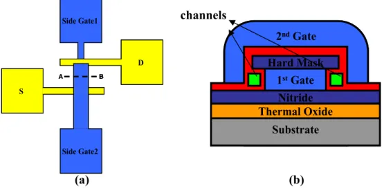
Figures 2-1(a) and (b) show the top and the cross-sectional views of the embedded NWTFT, respectively. From Fig.2-1(b), it can be seen that the two rectangular-shaped poly-Si NW channels are embedded snugly at the two sides of the gate structure capped with a nitride hardmask (HM). Fig.2-1(c) shows the enlarged view of the structural cross-section centered at one of the two NW channels showing the definition of channel thickness and width. In order to improve the device
performance, the channel thickness needs to be scaled into sub-40 nm regime [2-1]. Besides, the NW channels are sandwiched laterally by two independently biased gate electrodes. Such double-gate (DG) configuration allows high flexibility in device operation.
Fabrication flow of the NWTFT is illustrated in Figs. 2-2(a) ~ (f). The device fabrications in this thesis all started on 6-inch silicon wafers capped with 100-nm silicon dioxide. First, a layer of 50-nm nitride was deposited on the oxidized wafer. A gate stack which consists of 100-nm in situ-doped n+ poly (1st gate) and 50-nm
nitride (hard mask layer) was then deposited (Fig.2-2(a)). These stacked layers were all grown by low pressure chemical vapor deposition (LPCVD). Next, the gate stack was patterned by standard I-line lithographic and subsequent dry etching steps (Fig. 2-2(b)). Following the gate stack patterning, highly selective plasma etching was used for lateral etching of n+ poly-Si. These lateral cavities were formed at the two
sides of the gate stack structure while the remaining n+ poly-Si would serve as the
first gate once the device was completed (Fig. 2-2(c)). Afterwards, a 16.5nm-thick LP-TEOS oxide serving as the gate dielectric of the first gate and a 100-nm amorphous Si were deposited sequentially and then underwent an annealing at 600 ℃ in N2 ambient for 24 hours. After this solid phase crystallization (SPC) process, the
Next, the wafers were split into two groups receiving different S/D doping processes. In the first split, denoted as the implanted-S/D split, S/D doping was conducted by P+ implantation at energy of 15 keV with a dose of 5E15 cm-2 (Fig.
2-2(e)). The other split, the in situ doped-S/D split, the poly-Si layer was removed with an endpoint-mode dry etching to leave portion of the poly-Si at the sidewalls of the gate stack structure (Fig. 2-2(e-1-1)), followed by the deposition of 100 nm-thick
in situ doped n+ poly-Si (Fig. 2-2(e-1-2)).
After the aforementioned S/D doping process, an I-line lithographic step was then performed on the two splits to generate S/D photoresist patterns. NWs and S/D were defined simultaneously by a reactive plasma etching step. Note that this etching completely removed poly-Si film outside the hard mask and the portion that resided underneath the hard mask would remain intact forming a rectangular NW channel. Figures 2-2(f) and 2-2(f-1) illustrate the implanted-S/D and the in-situ-doped-S/D splits after this step. Another 14.5-nm LP-TEOS was deposited to serve as the 2nd
gate dielectric, followed by the deposition of a 100-nm in situ doped poly-Si which was subsequently patterned to form the 2nd gate electrode (Fig. 2-2(f)). All devices
were then covered with a 300-nm oxide passivation layer. Contact pads were thern formed with a standard metallization scheme. Before characterization, all devices received an 1-hour NH3 plasma treatment.
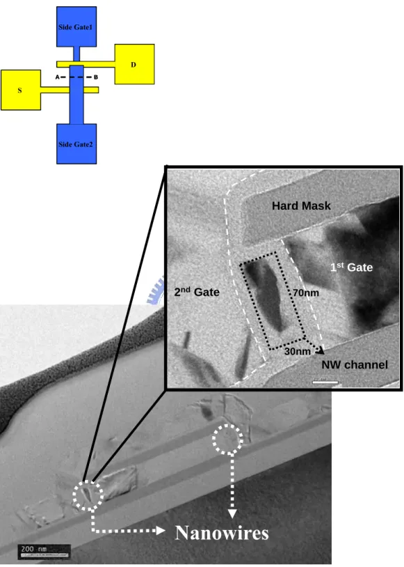
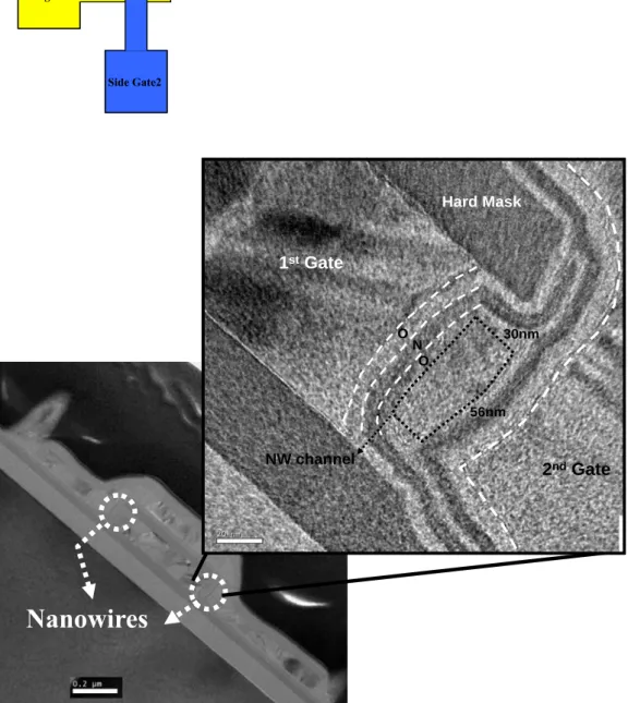
Figure 2-3 shows the cross-sectional TEM image of an embedded NW TFT device along the line AB shown in Fig.2-1(a). It could be seen that the shape of the nanowires was nearly rectangular. The sizes of channel height and thickness are approximately 70 nm and 30 nm, respectively.
2-2 Fabrication of NWTFT- SONOS Memory Devices
The structure of NWTFT SONOS memory device is identical to that of the embedded NWTFT except that an oxide-nitride-oxide (ONO) stack is used as the gate dielectric. The three layers in the ONO stack were deposited sequentially with LPCVD. Figures 2-4(a) and (b) show the schematics of the stack layer near the 1st gate or 2nd gate, respectively. For the gate dielectric of the 1st gate, the O/N/O consists of 5 nm LP-TEOS, 7 nm LP-silicon nitride, and 7 nm LP-TEOS. While for the gate dielectric of the the 2nd gate, the O/N/O consists of 5 nm LP-TEOS, 6.5nm LP-silicon nitride, and 8 nm LP-TEOS. Unlike the NWTFTs stated in the former section, the SONOS devices did not receive any plasma treatment before characterization.
The TEM image of a SONOS memory device is shown in Fig. 2-5. It is found that the channel thickness is 30 nm while the channel width is about 56 nm. Different composition in the ONO layer can be clearly recognized by the color
contrast in the gate dielectric. The dark region in the figure corresponds to the LP-silicon nitride layer.
2-3 The Measurement Setup
An automated system consisted of a semiconductor parameter analyzer-HP4156, a pulse generator Agilent-8110A, and a Visual Engineering Environment (VEE) was employed in this work to probe the electrical characteristics. These equipments integrated in the system were controlled with the interactive characterization software (ICS) program. During the measurements a dehumidifier was used to keep the humidity at the same level, while the temperature was also accurately controlled by a temperature regulated heater.
Because all test devices are double-gated, several modes of operations could be implemented. In this thesis, the 1st gate is defined as SG-1 gate and the 2nd gate as
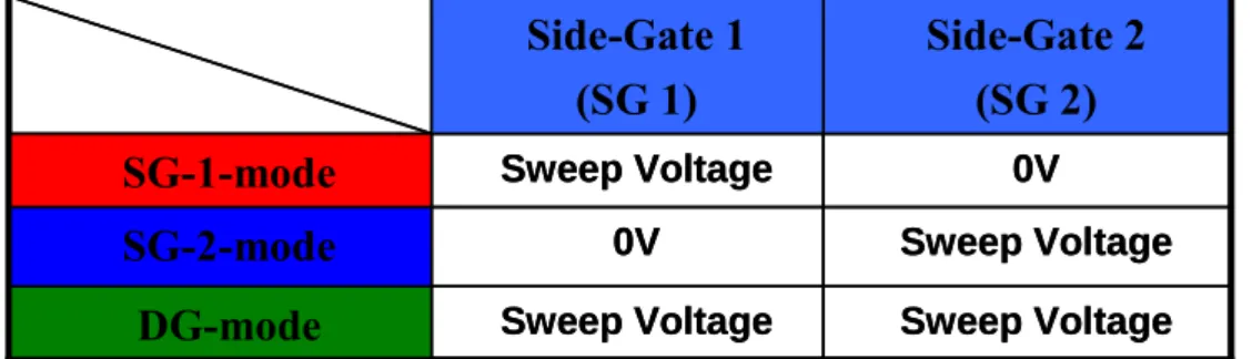
SG-2 gate. The SG-1-mode of operation refers to the mode when the sweeping voltage (serving as the driving gate) is applied to the SG-1 gate while SG-2 gate is grounded. The SG-2-mode of operation interchanges the bias condition applied to the two gates in SG-1 mode. The DG-mode refers to the operation when the two gates are connected together to serve as the driving gate. Table 2-1 summarizes the conditions of the three operation modes.
The performance parameters of the NW devices such as subthreshold swing (S.S.) and threshold voltage (Vth) are extracted from the ID-VG curve at VD = 0.5 V. The
definition of these parameters is as follows:
Subthreshold swing (S.S.) can be calculated from the diffusion-dominated current in the weak region by
1 10 ) (log . . − ⎟⎟ ⎠ ⎞ ⎜⎜ ⎝ ⎛ ∂ ∂ = G D V I S S (mV/dec) (2-1)[1-3]. Threshold voltage (Vthc) is calculated by constant current method,
nA L W I V Vthc = G@ D = ×10 (V) (2-2)[2-2], in which W and L are the channel width and length, respectively.
Another major parameter is the series resistance (Rseries) which is extracted from
the ID-VD curve [2-3]. It requires a set of devices with the same channel width but different channel length. In this approach, VD/ID ratio measured at a fixed VD of 0.1
V and VG -Vthc ranging from 0.1 V to 0.5 V as a function of drawn channel length
(Lmask) for devices with various channel width. Each curve can be fitted with a line
and all lines intersect at a common point. The values of intercepts with two axis are Rseries and ΔL: R A(L L) I V R series mask D D channel = = + −Δ (Ω) (2-3)[2-3]
Chapter3
Effects of Operational Modes, Gate Dielectric
Materials, and Source/Drain Doping Processes
on Device Characteristics
3-1 Characteristics of NW Devices with Implanted
Source/drain
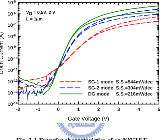
Typical ID-VG characteristics of NW TFTs with implanted S/D are shown in Fig. 3-1. Channel length of the device is 1 m, and the NW thickness is 30 nm. The measurements were performed at VD = 0.5 and 2 V. The gate dielectric is TEOS
CVD oxide, and the device characterized in Fig.1 is with the 1st gate oxide thickness
of 14.5nm and the 2nd gate oxide thickness of 16.5nm. Ideally, SG-1 and SG-2
modes of operation are expected to display identical characteristics based on the nearly symmetric structure of NW, but obviously the expectation fails to realize in the figure. It is seen that the SG-2 mode exhibits better performances in terms of larger ON current, less OFF current, and smaller S.S, as compared with the SG-1 mode.
Such disparities in the transfer characteristics can be attributed to the different conduction path of carriers during device operation. To make it clear, in Fig. 2(a) we plot the top view of the device structure and Fig. 2(b) the cross-sectional view of
the device along the C-D lines shown in Fig. 2(a). During SG-1 mode of operation, the conduction electrons have to transport across the offset (i.e., ungated) regions between the S/D and the inner conduction channels, therefore the S/D series resistance is increased. Furthermore, the overlap area between the 2nd gate and
source/drain is obviously larger than that of the 1st gate. Considering the low
implant energy executed in the S/D step, the portions of the S/D regions near the channel are expected to be with a low dopant concentration. The larger overlapping of the 2nd gate tends to reduce the parasitic S/D resistance during the SG-2 mode of
operation. Accounting for the aforementioned two factors, a much higher ON current of SG-2 mode over SG-1 mode becomes reasonable.
The ungated regions illustrated in Fig. 2(b) also degrade the S.S. of the SG-1 mode of operation. As can bee seen in Fig.1, the S.S. is 544 mV/dec for SG-1 mode and is improved to 304 mV/dec for SG-2 mode. This is because the existence of the ungated regions between the source and the channel introduces a parasitic barrier for carriers to be injected from the source to the channel. The parasitic barrier needs a higher gate voltage to suppress and thus the S.S. is degraded.
In Fig. 1, we can also see that the device characteristics can be significantly improved with the double-gated scheme. In addition to exhibiting the largest ON current, the DG mode also shows the smallest S.S. (216 mV/dec) and threshold
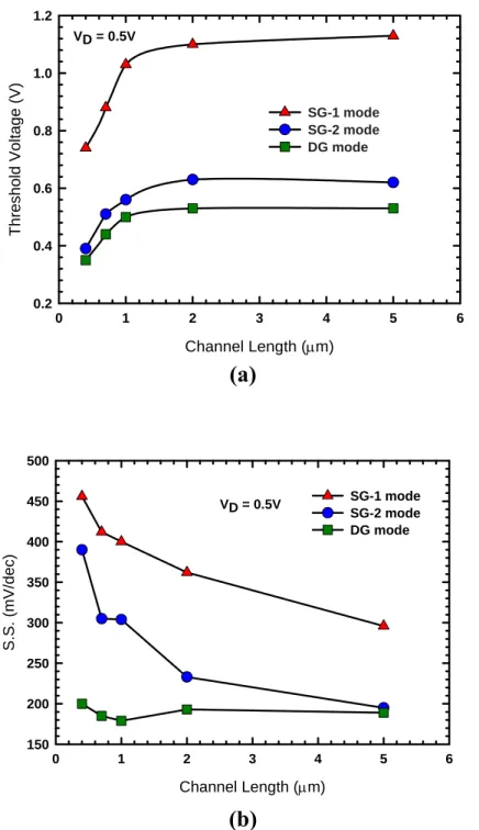
voltage (Vth) among the three modes. Figure 3-3(a), (b) show the Vth roll-off and
subthreshold swing characteristics, respectively, under different operational modes for devices with channel length of 5 μm, 2 μm, 1 μm, 0.7 μm and 0.4 μm. The threshold voltage is extracted at VD = 0.5V. Not only Vth roll-off but also S.S. degradation
shows with scaling down the devices. Apparently the DG mode is much superior to the two single-gate modes in reducing the short channel effect (SCE).
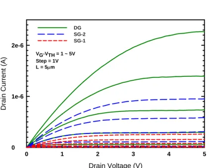
Fig. 3-4 displays the drain current as a function of drain voltage. In the measurements gate overdrive (VG-VTH) is varied from 1 to 5 V. It is interesting to
see that the ON current of DG mode is actually larger than the sum of the ON currents of SG-1 and SG-2 modes, as shown in Fig. 3-5. Possible origins for this observation are the significant reduction of resistance and the possible occurrence of volume inversion effect. The latter phenomenon has been reported to commonly occur in devices with ultra-thin body and multiple-gate devices [3-1].
3-2 Effects of ONO Gate Dielectric on Device
Characteristics
When we replace the gate dielectric with the ONO stack layer, the device depicts some improvements in comparison with devices characterized in previous section. The cross-sectional TEM images of two different devices are illustrated previously in
Fig. 2-3 and 2-5. The NW channel body thickness of the two splits is almost equal and around 30 nm. The thickness of O/N/O stack layer is 5 nm/7 nm/7 nm for the gate dielectric of the 1st gate, and 5 nm/6.5nm/8 nm for the 2nd gate. The estimated
equivalent oxide thickness (EOT) is 15.6 nm for the 1st gate and 16.4 nm for the 2nd
gate. Table 3-1 briefly summarizes these devices with different gate dielectric.
The transfer characteristics of a NW device with ONO dielectrics are shown in Fig. 3-6. Compared with the SG-1 mode of operation of the oxide split shown in Fig. 3-1, the S.S. is promoted from 544 mv/dec to 233 mv/dec for the ONO device shown in this figure, although the two devices have almost the same EOT (Table 3-1). Besides, the characteristics of SG-1 mode and SG-2 mode look much more symmetric in the present case. For DG-mode, the value of S.S. can be less than 100 mV/dec with ONO gate dielectrics. Such improvements are postulated to be due to the additional passivation effect by the high hydrogen content contained in the nitride film which can effectively reduce the amount of active defects presenting inside the poly-Si NW and at Si/SiO2 interface. The high hydrogen content in the nitride layer
is related to the use of H-related reaction gases during deposition, e.g., SiH4 and NH3
3-3 Effects of in situ Doped Source/Drain on Device
Characteristics
Figure 3-7 is the characteristics of an NW device with in-situ doped S/D. The gate dielectrics are ONO identical to the devices characterized in last section, so here we can investigate and understand the difference between different S/D schemes by comparing Fig. 7 with Fig. 6. Obviously, the device performance is further enhanced with the implementation of in situ doped S/D. In DG mode, the S.S. of the device with implanted S/D is 89 mV/dec. For in-situ doped S/D, it is improved to 73 mV/dec. To more clearly illustrate the impacts, these ID-VG curves are plotted together in Fig. 3-8. As can be seen in the figure, for each operation mode the in-situ doped S/D split always exhibits larger ON current than the implanted-S/D counterpart. In addition, the OFF current is also dramatically reduced with in-situ doped S/D, resulting in a high ION/IOFF ratio of around 108, which is one order of magnitude larger
than the device with implanted S/D.
Statistical analysis and comparison of ION-IOFF characteristics between implanted
and in-situ doped S/D splits are shown in Fig. 3-9. In this figure ION is the current
measured at VG = 5 V and VD = 2 V and IOFF is the minimum current. According to
the result, the enhancement of ION at IOFF = 2 x 10-13 A is about 1.4X with the in-situ
given in Fig. 3-10, again demonstrating much reduced series resistance with in-situ doped S/D.
The reason for these improvements can be explained as follows: In the implanted split, S/D regions were formed by a low-energy ion implantation such that dopants were situated near the top surface and would not dope the NW channel. Though this method attains good gate controllability over NW channels, it is achieved at the expense of an increase in S/D resistance as only a small portion of S/D (upper portion) is heavily doped, and insufficient doping of the S/D regions close to the channel is expected. Such issue is resolved with the in-situ doped scheme where almost the whole S/D regions including those close to the channel are heavily doped, thus ON current is improved. To confirm this point, S/D series resistance is extracted using linear regression method, and the results are shown in Fig. 3-11. It is seen that the series resistance is 45 kΩ for the implanted splits (Fig. 3-11 (a)), and significantly improved to 8.1kΩ with in-situ doped S/D (Fig. 3-11(b)).
In a previous paper [3-3], the off-state leakage current has be found to be the gate-induced drain leakage (GIDL) component which is also closely related to the dopant concentration of deep S/D region. With the high dopant concentration pertaining to the in-situ doped S/D, the GIDL can be suppressed, as evidenced in Fig. 3-7.
Chapter4
Characteristics of Nanowire TFT-SONOS
Memory
4-1 Program/Erase Operation Principles and
Characteristics
For non-volatile memory (NVM), it usually refers to the “0” state or “1” state by modulating the threshold voltage (Vth) via trapping or de-trapping of carriers in the
storage layer. The program/erase (P/E) mechanisms briefly include channel-hot-electron injection (CHEI), Fowler-Nordheim tunneling (FN tunneling) and band-to-band tunneling (BTBT). The CHEI method is appropriate for programming operation of the NOR flash but not suitable for the TFT-SONOS memory in this thesis [4-1]. Owing to the grain boundaries contained in the poly-Si NW channels which would scatter the transporting electrons, it is difficult to have electrons possessing sufficient energy to cause impact ionization with an acceptable programming bias condition. Hence the memory devices in this chapter are programmed and erased by FN tunneling.
Fig. 4-1(a), (b) illustrate the energy band diagrams of the programming operation with the FN tunneling mechanism. Fig. 4-1(a) represents the band diagram in the
flat-band condition where qφ1 =3.1eVand qφ2 =1.05eV are the barrier height of conduction band between oxide and Si substrate, and between nitride and oxide, respectively. When applying a highly positive voltage to the control gate with source and drain grounded to render the electric field larger than
ox
t qφ1
, a large amount of electrons in the channel can tunnel through the oxide and then be trapped in the nitride layer, as shown in Fig. 4-1(b) [4-2]. The erasing operation is to de-trap electrons from the nitride layer to the channel by biasing the control gate with a highly negative voltage.
As shown in previous chapter that the 1st gate shows poorer gate controllability
than the 2nd one due to the existence of the ungated channel regions. Therefore, in
the following analysis the 2nd gate is employed as the major control gate to which a
high voltage is applied for manipulating the P/E operations, while an auxiliary voltage would be applied to the 1st gate to help optimize the P/E efficiencies. Figure 4-2 (a)
is the schematic of the proposed NW SONOS with an ONO gated with the 2nd gate
and an oxide gated with the 1st gate. According to the results of one of our previous
studies, the small volume NW channel with independent gates, P/E efficiency can be affected by the bias voltages applied to the two independent gates [4-3]. Fig. 4-2 (b) shows the transfer ID-VG curves of one programmed and two erased states. The O/N/O consists of 5 nm LP-TEOS, 6.5nm LP-silicon nitride, and 8 nm LP-TEOS and channel
body thickness is 30nm. The programmed state is obtained with programming voltages of VSG-1 / VSG-2= 5V/15V and programming time (tP) = 1 ms, while the two
different erasing states are obtained with the following two erasing condition: (1) VSG-1 / VSG-2= 5V/-9V, erasing time (tE) = 100 ms; and (2) E1: VSG-1 / VSG-2= 8V/-9V,
tE = 100 ms. It can be seen that the applied 1st-gate bias can indeed affect the Vth shift.
The memory window enlarges from 0.23 V to 0.41 V with the 1st-gate bias varied
from 5 V to 8 V. The programming and erasing characteristics as a function of time are shown in Figs. 4-3 (a) and (b), respectively. In Fig. 4-3(a) the programming efficiency can be enhanced by applying a positive voltage to the 1st-gate. In the
figure VSG-2= 15 V and ΔVth is around 3 V after 5 ms (point A) for VSG-1= 0 V, and
improves to 0.5 ms (point B) for VSG-1= 5 V. This is because by applying a positive
voltage during programming, more electrons could be generated in NW channel. For erasing characteristics shown in Fig. 4-3(b) with VSG-1 =-9 V, an increase in VSG-1 also
improves the erasing efficiency. As can be seen in the figure, the erasing state at the VSG-1 / VSG-2= 8 V/-9 V is the fastest erasing condition. Note the conditions with
VSG-1 = 0 V or 5 V, the curves exhibit saturation phenomenon as erasing time is larger
than 1 ms. This is postulated to be caused by the electron injection from the 2nd gate.
Nonetheless, such phenomenon is absent with VSG-1 = 9 V. More efforts are in
4-2 Reliability Characteristics and Issues
The reliability of memory devices is also crucial for practical applications. Data retention for commercial memories refers to the ability to keep trapped charges from loss after ten years at a temperature range from 0 °C to 85 °C [4-4]. The migration of lost charge includes thermal excitation (TH), trap-to-trap tunneling (TT), band-to-trap tunneling (BT), trap-to-band tunneling (TB) and Frenkel-Poole emission (FP). The tunneling mechanisms consider tunneling of the trapped electrons in the nitride back to the conduction band of Si substrate or to the interface traps at Si channel/oxide interface [4-4]. The Frenkel-Poole emission is the movement of trapped charges from site to site with levels inside the bandgap of the nitride [4-5]. Details about the data lost paths are shown in Fig. 4-4.
During the retention measurements, all S/D and gates electrodes are grounded at room temperature. Figure 4-5 depicts the retention characteristics of the embedded NW-SONOS device. The window size at the beginning is about 0.83 V and after 10 years it is about 0.78 V. It seems that the capability of data retention can be further promoted. The thickness of tunneling oxide for memory devices is 5 nm which can efficiently stop charges escaping by direct tunneling. Moreover, the shape of NW channels is rectangular which depresses the irregular electric field occurring in the corners and suppresses the field-enhanced trap-assisted tunneling. Consequently,
Frenkel-Poole emission through oxide-trap is considered to be the major loss mechanism in this device and can sustain almost the same specific window after a long duration.
Endurance is another important reliability topics, which is a measure of the number of program/erase (P/E) cycles that the device will still work without failure. The commercial specification for available NVM products is 106 P/E cycle times
[4-6]. Fig. 4-6(a) and (b) are the endurance characteristics expressed with I-V transfer curves and Vth variation as a function of P/E cycles. The bias condition for programming states is VSG-1 / VSG-2= 8 V/13 V, and tP = 1 ms, and for erasing states is
VSG-1 / VSG-2= 8 V/-9 V, and tE = 100 ms. With increasing P/E cycle, the Vth for both
program-state and erase-state moves upward and the memory window narrows. The transfer curves are recorded after 1, 50, and 200 P/E cycles. The memory window moves rightward and the S.S. is gradually degraded. Since the device is stressed with high voltage conditions, the energetic carriers would cause damage in the tunneling oxide and more and more oxide traps and interface states would be generated, resulting in the degradation of the performance. Certainly the oxide quality is an important parameter of the endurance.
4-3 Effects of NW Channel Thickness
Figure 4-7 illustrates the structural cross-section of NW-SONOS devices in which the channel thickness is defined. Since the poly-Si NW channel thickness of the devices characterized in this thesis can be controlled by tuning the lateral etching time of the 1st gate in the fabrication (see Chap. 2). To study the effect of the NW
channel thickness we have fabricated NW-SONOS devices with two splits of lateral etching time, namely, 6 sec and 12 sec. Unlike the device structure presented in previous section, in this study the ONO layer is gated with the 1st gate. Thus, the high
voltage during P/E operations is applied to the 1st gate.
Figures 4-8(a) and (b) show the transfer characteristics of devices with NW channel thickness of 10 and 50 nm, respectively. The programming condition is VSG-1 / VSG-2= 15 V/5 V with tP of 1 ms. In Fig. 4-8(a), after programming the
window (ΔVth) of SG1-mode is 1.8 V. While using SG-2 mode or DG-mode as the
read mode, the ΔVth for the two modes are both about 1.4 V. In contrast, in Fig.
4-8(b) we can see that, although a window of 2 V is achieved for SG-1 mode, it’s just only 0.6 V for SG-2 and DG modes. Besides, the subthreshold leakage is obviously larger as the NW channel thickness is larger. The above results clearly indicate that a reduction in the NW thickness would enhance the gate controllability and coupling effect of the two gates. Fig. 4-9 is the programming characteristics with different
channel body thickness under VSG-1 / VSG-2= 15 V/5 V. The programming efficiency
Chapter5
Conclusions and Future Work
5-1 Conclusions
In this study, a novel poly-Si NW TFT with a simple fabrication process is proposed and successfully developed. Equipped with the independent double-gated structure, impressive device performance is obtained and effective threshold voltage modulation is demonstrated, which profoundly increases the flexibility of device operation. By substituting ONO stack layer for silicon dioxide as gate dielectric, the gate controllability is improved which is postulated to be due to the passivation of channel defects with the hydrogen species contained in the nitride layer. Furthermore, by employing in-situ doped poly-Si as S/D, we demonstrate a high performance double-gated NW TFT with much reduced series resistance. Significant improvement in on-current and S.S. as low as 73 mv/dec are achieved. Throughout the whole fabrication process, no advanced lithography tools are required. The proposed NW devices show promising potential for reducing operation voltage and power consumption in practical applications with a low fabrication cost.
Regarding the NW TFT-SONOS memory, the independent double-gated structure provides flexibility for programming and reading operation. Moreover, the
results indicate that, by applying an adequate auxiliary gate (i.e., other than the write gate) bias, the programming and erasing efficiency are both enhanced. The data retention can be promoted as compared with the former work with triangle NW channel. This is attributed to the rectangular shape of NW channels of the proposed devices which may suppress the irregular electric field in the corner and thus can effectively keep trapped charges from escaping by field emission. The memory devices with thinner channel body can also improve the programming efficiency and has more flexible reading modes.
5-2 Future Work
The preliminary investigation of embedded NW TFT devices and the application of the novel DG structure to SONOS memory are carried out in this thesis. The following topics can be further addressed. First, the substitution of the gate oxide by high-κ material may improve the gate controllability of 1st gate and 2nd gate.
The high-κ material provides a thin EOT thus the gate controllability and subthreshold swing of the devices can be further improved. In this regard, atomic-layer deposition (ALD) technique is suitable for the 3D NW device fabrication since it can provide conformal thin film deposition.
performance. In this work, the poly-Si channel is formed by solid-phase crystallization (SPC) during the device fabrication, and the resultant grain size is small. By using the excimer laser annealing (ELA) or metal-induced lateral crystallization (MILC) methods to enlarge the grain, we expect that the device performance can be further enhanced.
For memory characterization, the erasing efficiency and the recognized window are poor in this study. P/E efficiency can be improved by further thinning the channel body. Furthermore, the use of high-κ materials as the tunneling oxide or block oxide may be helpful for improving performance. The optimization of the high-κ structure and improvement of its quality worth more efforts to advance the NW device technology.
References
[1-1] Amitava DasGupta, “Multiple Gate MOSFETs The Road to the Future,”
IWPSD 2007, pp.96-101(2007).
[1-2] S. Thompson, P. Packan, and M. Bohr., “MOS Scaling: Transistor
Challenges for the 21st Century,” Intel Technology Journal(1998).
[1-3] Y. Taur and T. H. Ning, “Fundamentals of Modern VLSI
Devices.”Cambridge, U.K.: Cambridge Univ. Press (1998).
[1-4] Y.-K. Choi, N. Lindert, P. Xuan, S. Tang, D. Ha, E. Anderson, T.-J. King, J. Bokor, and C. Hu, “Sub-20nm CMOS FinFET Technologies,” IEDM Tech.
Dig., pp. 421-424(2001).
[1-5] T. Sekigawa and Y. Hayashi, “Calculated Threshold-Voltage
Characteristics of an XMOS Transistor Having an Additional Bottom Gate,” Solid State Electron. 27, 827(1984).
[1-6] M. Ieong, H.-S. P. Wong, Y. Taur, P. Oldiges, and D. Frank, “DC and AC
Performance Analysis of 25 nm Symmetric/Asymmetric Double-Gate, Back-Gate and Bulk CMOS,” SISPAD, pp. 147–150(2000).
[1-7] B. Doyle, B. Boyanov, S. Datta, M. Doczy, S. Hareland, B. Jin, J. Kavalieros, T. Linton, R. Rios, and R. Chau, “Tri-Gate Fully-Depleted CMOS
133–134(2003).
[1-8] Fu-Liang Yang , Hao-Yu Chen, Fang-Cheng Chen, Cheng-Chuan Huang, Chang-Yun Chang, Hsien-Kuang Chiu, Chi-Chuang Lee, Chi-Chun Chen, Huan-Tsung Huang, Chih-Jian Chen, Hun-Jan Tao, Yee-Chia Yeo, Mong-Song Liang, Chenming Hu, “25nm CMOS Omega FETs,” IEDM Tech. Dig.,
pp.255-258(2002).
[1-9] N. Singh, A. Agarwal, L. K. Bera, T. Y. Liow, R. Yang, S. C. Rustagi, C. H. Tung, R. Kumar, G. Q. Lo, N. Balasubramanian, and D. L. Kwong,
“High-Performance Fully Depleted Silicon Nanowire (Diameter ≤ 5 nm) Gate-All-Around CMOS Devices,” IEEE Electron Device Lett., Vol.27, No.5, pp.383-386(2006).
[1-10] F. L. Yang, D. H. Lee, H. Y. Chen, C. Y. Chang, S. D. Liu, C. C. Huang, T. X. Chung, H. W. Chen, C. C. Huang, Y. H. Liu, C. C. Wu, C. C. Chen, S. C. Chen, Y. T. Chen, Y. H. Chen, C. J. Chen, B. W. C. P. F. Hsu, J. H. Shieh, H. J. Tao, Y. C. Yeo, Y. Li, J. W. Lee, P. Chne, M. S. Liang, and C. Hu, “5
nm-gate Nanowire FinFET,” Tech. Dig. VLSI Technol., pp. 196–197(2004).
[1-11] R. Agarwaland C.M. Lieber, “Semiconductor Nanowires: Optics and
[1-12] M. Law, L. E. Greene, J. C. Johnson, R. Saykally and P. Yang, “Nanowire
dye-sensitized solar cells,” Nature Materials 4, pp.455-459(2005).
[1-13] S. Pal, E. C. Alocilja, and F. P. Downes, “Nanowire Labeled Directcharge
Transfer Biosensor for Detecting Bacillus Species,” Biosens. Bioelectron., Vol. 22, pp. 2329–2336(2007).
[1-14] J. P. Colinge, M. H. Gao, A. R. Rodriguez, H. Maes, and C. Claeys,
“Silicon-on-insulator: gate-all-around device,” IEDM Tech. Dig., pp.
595–598(1990).
[1-15] M. H. White, Y. Yang, A. Purwar, and M. L. French, “A Low Voltage
SONOS Nonvolatile Semiconductor Memory Technology,” IEEE Int’l Nonvolatile Memory Technology Conference, 52(1996).
[1-16] A. M. Morales and C. M. Lieber, “A Laser Ablation Method for the
Synthesis of Crystalline Semiconductor Nanowires,” Science, Vol. 279,
No. 5348, pp. 208–211, Jan.(1998).
[1-17] C. M. Lieber and Z. L. Wang, “Functional nanowires,” MRS Bull., Vol. 32,
No. 2, pp. 99–108(2007).
[1-18] R. S. Wagner and W. C. Ellis, “Vapor-Liquid-Solid Mechanism of Single
[1-19] Y. Wu., P. Yang, “Direct Observation of Vapor−Liquid−Solid Nanowire
Growth,” J. Am. Chem. Soc., 123 (13), pp 3165–3166(2001).
[1-20] Kinam Kim, Jung Hyuk Choi, Jungdal Choi, Hong-Sik Jeong , “The Future
Prospect of Nonvolatile Memory,” IEEE VLSI-TSA. Int. Symp. On,
pp.88-94 (2005).
[1-21] M. H. White, D. A. Adams, J. Bu, “On the Go with SONOS,” IEEE Circuits
& Devices, pp.22-31(2000).
[1-22] H. T. Lue, S. Y. Wang, E. K. Lai, Y. H. Shih, S. C. Lai, L. W. Yang, K. C. Chen, Joseph Ku, K.Y. Hsieh, Rich Liu, and C. Y. Lu, “BE-SONOS: A
Bandgap Engineered SONOS with Excellent Performance and Reliability,” IEDM Tech. Dig., session 22.3(2005).
[1-23] C. H. Lee, K. I. Choi, M. K. Cho, Y. H. Song, K. C. Park, K. Kim, “A Novel
SONOS Structure of SiO2/SiN/Al2O3 with TaN Metal Gate for Multi-Giga Bit Flash Memeries,” IEDM Tech. Dig., session 26.5( 2003). [1-24] A.J. Walker, S. Nallamothu, E.-H. Chen, M. Mahajani, S.B. Herner,
M. Clark, J.M. Cleeves, S.V. Dunton, V.L. Eckert, J. Gu, S. Hu, J. Knall, M. Konevecki, C. Petti, S. Radigan, U. Raghuram, J. Vienna, M.A. Vyvoda, “3D
TFT-SONOS Memory Cell for Ultra-High Density File Storage Applications,” Tech. Dig. VLSI Technol., pp.29-30(2003).
[1-25] H. C. Lin, M. H. Lee, C. J. Su, and S. W. Shen, “Fabrication and
Characterization of Nanowire Transistors with Solid-Phase
Crystallized Poly-Si Channels,” IEEE Trans. Electron Devices, Vol. 53, pp. 2471-2477(2006).
[1-26] H. C. Lin, H. H. Hsu., C. J. Su. and T. Y. Huang , “A Novel Multiple-Gate
Polycrystalline Silicon Nanowire Transistor Featuring an Inverse-T Gate,” IEEE Trans. Electron Devices, Vol. 19, pp.718-720(2008).
[2-1] H. C. Lin, W. C. Chen, C. D. Lin, and T. Y. Huang, “Performance
Enhancement in Double-Gated Poly-Si Nanowire Transistors with Reduced Nanowire Channel Thickness,” IEEE Electron Devices Lett., vol.30, pp.644-646(2009).
[2-2] T. Hiramoto and M. Takamiya, “Low Power and Low Voltage MOSFETs
with Variable Threshold Voltage Controlled by Back-Bias”, IEICE Ttans.
Electron., Vol. E83-C, pp.161-169(2000).
[2-3] S. E. Laux, “Accuracy of an Effective Channel Length/External
Resistance Extraction Algorithm for MOSFET's,” IEEE Trans. Electron
Devices, Vol. 31, pp. 1245-1251(1984).
[3-1] S. Venkatesan, G. W. Neudeck, and R. F. Pierret, “Dual-gate Operation and
Lett., Vol. 13, pp.44-46(1992).
[3-2] C. Y. Lu, H. C. Lin, Y. J. Lee and C. C. Chao, “Impacts of SiN-Capping
Layer on the Device Characteristics and Hot-Carrier Degradation of
nMOSFETs,” IEEE Trans. Device and Materials Reliability, Vol.7,
pp.175-180(2007).
[3-3] H. C. Lin, M. H. Lee, C. J. Su and H. W. Shen, “Fabrication and
Characterization of Nanowire Transistors with Solid-Phase Crystallized Poly-Si Channels,” IEEE Trans. Electron Devices, Vol.53, pp. 2471-2477 (2006).
[4-1] B. Eitan, P. Pavan, I. Bloom, E. Aloni, A. Frommer, and D. Finzi, “NROM: A
Novel Localized Trapping, 2-bit Nonvolatile Memory Cell,” IEEE Electron
Device Lett., Vol. 21, pp. 543–545, Aug. (2000).
[4-2] K. F. Schuegraf and C. Hu, “Hole Injection SiO2 Breakdown Model for Very Low Voltage Lifetime Extrapolation, ” IEEE Trans. Electron
Devices, Vol. 41, pp. 761-767, (1994).
[4-3] H. C. Lin , H. H. Hsu , C. J. Su , T. Y. Huang , “A Novel Multiple-Gate
Gate,” IEEE Electron Device Lett., Vol. 29, pp. 718–720, (2008). [4-4] Y. Yang, and M. H. White, “Charge Retention of Scaled SONOS
Nonvolatile Memory Devices at Elevated Temperatures”, Solid-State
Electronics, Vol. 44, pp. 949-958 (2000).
[4-5] K. Lehovec and A. Fedotowsky, “Charge Retention of MNOS Devices
Limited by Frenkel–Poole Detrapping,” Appl. Phys. Lett., Vol. 32, No. 5, pp.
335-338 (1978).
[4-6] K. Kim and J. Choi, “Future Outlook of NAND Flash Technology for
40nm Node and Beyond,” Non-Volatile Semiconductor Memory Workshop,
(a) Side Gate1 D S Side Gate2 A B Side Gate1 Side Gate1 Side Gate1 D D D SSS Side Gate2 Side Gate2 A B A B Substrate Thermal Oxide 1stGate Nitride Hard Mask 2ndGate Substrate Thermal Oxide 1stGate Nitride Hard Mask 2ndGate channels (b)
Fig. 2-1 (a) The layout and (b) Cross-sectional view of embedded NWTFT.
(b) Definition of 1st gate. Si Sub Thermal Oxide HM Gate Poly-Si Si Sub Thermal Oxide HM Gate Si Sub Thermal Oxide Thermal Oxide HM Gate Poly-Si (c) Lateral etching. Thermal Oxide Nitride Gate HM Si sub Thermal Oxide Thermal Oxide Nitride Si Sub Thermal Oxide Gate HM HM Si sub Si Sub Thermal Oxide Nitride Gate HM Si Sub Thermal Oxide Thermal Oxide Nitride Gate HM (d) SPC. Nitride Gate Si Sub Thermal Oxide Thermal Oxide Gate Nitride HM
HM
(e) S/D ion implantation.
Si Sub Thermal Oxide Gate Si Sub Thermal Oxide HM Gate Thermal Oxide HM Si Sub Thermal Oxide Gate Si Sub Thermal Oxide HM Gate Thermal Oxide
(e-1-1) Etching poly-Si.
HM Gate In-situ doped poly
Si Sub Thermal Oxide HM Si Sub Thermal Oxide Gate Si Sub Thermal Oxide HM Gate In-situ doped poly
Thermal Oxide
HM Gate Source
Drain
(f) Definition of S/D and formation of NW channel. (implanted S/D type)
(f-1) Definition of S/D and formation of NW channel. (in situ doped S/D type)
Fig. 2-2
Si Sub Thermal Oxide Si Sub Thermal Oxide HM Gate Source Drain Thermal Oxide Si Sub Thermal Oxide HM Gate Source Drain Si Sub Thermal Oxide HM Gate Si Sub Thermal Oxide Thermal Oxide HM Gate Source Drain Drain Gate Si Sub Thermal Oxide Source Poly-Si NW Channel Gate Si Sub Si Sub Thermal Oxide Drain Gate Thermal Oxide Source Poly-Si NW Channel Gate Drain Gate Source Poly-Si NW Channel GateSide Gate1
Fig. 2-3 Cross-sectional TEM image of embedded NW TFT and NW channel profile along line AB of the layout.
Side Gate1 D S Side Gate2 A B Side Gate1 Side Gate1 D D D SSS Side Gate2 A B A B Side Gate2 Hard Mask 2ndGate 1stGate NW channel 30nm 70nm Hard Mask 2ndGate 1stGate NW channel 30nm 70nm
Nanowires
(a) NWTFT-SONOS memory with the ONO storge layer near 1st gate.
Substrate Thermal oxideNitride
Gate
Gate Hard Mask
Substrate Thermal oxideNitride
Gate Gate Hard Mask Gate Hard Mask Substrate Thermal oxide Gate Nitride Hard Mask Gate Substrate Thermal oxide Gate Nitride Hard Mask Gate
(b) NWTFT-SONOS memory with the ONO storge layer near 2nd gate.
Fig. 2-4
Table 2-1 Summary of the conditions of the three operation modes.
Sweep Voltage Sweep Voltage DG-mode Sweep Voltage 0V SG-2-mode 0V Sweep Voltage SG-1-mode Side-Gate 2 (SG 2) Side-Gate 1 (SG 1) Sweep Voltage Sweep Voltage DG-mode Sweep Voltage 0V SG-2-mode 0V Sweep Voltage Side-Gate 1 (SG 1) Side-Gate 2 (SG 2) SG-1-mode
Side Gate1
Fig. 2-5 Cross-sectional TEM image of the NWTFT-SONOS memory device and NW channel profile along line ABof the layout.
Side Gate1 D S Side Gate2 A B Side Gate1 Side Gate1 D D D SSS Side Gate2 A B A B Side Gate2 1stGate 2ndGate Hard Mask O N O
Nanowires
NW channel 30nm 56nm 1stGate 2ndGate Hard Mask O N O NW channel 30nm 56nm 1stGate 2ndGate Hard Mask O N O NW channel 30nm 56nmGate Voltage (V) -2 -1 0 1 2 3 4 5 Dra in Cu rrent (A) 10-14 10-13 10-12 10-11 10-10 10-9 10-8 10-7 10-6 10-5 SG-1 mode S.S.=544mV/dec SG-2 mode S.S.=304mV/dec DG mode S.S.=216mV/dec VD = 0.5V, 2 V L = 1μm
C D
(a)
2nd Gate 1st Gate Source or Drain Thermal Oxide Si Substrate(b)
Fig.3-2 (a) Top view of the NW device, and (b) cross-sectional view of
the device along the C–D lines shown in (a). Projection of the second
gate (shaped by the dashed lines) is also shown. From the figure, it
can be seen that ungated regions (indicated by the double-head
arrows) exist between the inner conduction channel (gated by the
Channel Length (μm) 0 1 2 3 4 5 6 Thresho ld Volta ge (V) 0.2 0.4 0.6 0.8 1.0 1.2 SG-1 mode SG-2 mode DG mode VD = 0.5V
(a)
Channel Length (μm) 0 1 2 3 4 5 6 S. S. (mV/dec) 150 200 250 300 350 400 450 500 SG-1 mode SG-2 mode DG mode VD = 0.5V(b)
Fig. 3-3 (a) V
thand (b) subthreshold swing of the NW devices under
Drain Voltage (V)
0 1 2 3 4 5
Drain Current (A)
0 1e-6 2e-6 DG SG-2 SG-1 VG-VTH = 1 ~ 5V Step = 1V L = 5μm
Fig. 3-4 Output characteristics of an NW TFT under various
operation modes.
Drain Voltage(V) 0 1 2 3 4 5 Drain Cur rent (A) 0 1e-6 2e-6 DG SG-1 +SG-2 VG-VTH = 1V L = 5μmFig. 3-5 Comparisons of output drain current of DG mode with the
sum of SG-1 and SG-2 modes.
5/6.5/8nm, EOT =16.4nm 16.5nm 5/7/7nm, EOT =15.6nm 14.5nm 30nm 30nm
Channel body thickness
ONO stack layer oxide
2ndgate dielectric
ONO stack layer oxide 1stgate dielectric
Type B
Type A
5/6.5/8nm, EOT =16.4nm 16.5nm 5/7/7nm, EOT =15.6nm 14.5nm 30nm 30nmChannel body thickness
ONO stack layer oxide
2ndgate dielectric
ONO stack layer oxide
1stgate dielectric
Type B
Type A
Table 3-1 Summary of the two types of devices with different gate
dielectrics. Type-A devices have silicon dioxide as gate dielectrics,
while Type-B devices have ONO.
Gate Voltage (V) -1 0 1 2 3 4 5 Dra in Cu rrent (A) 10-13 10-12 10-11 10-10 10-9 10-8 10-7 10-6 10-5 SG-1 mode SG-2 mode DG mode VD= 0.5, 2V L= 1μm S.S.~89mV/dec
Fig. 3-6 Transfer characteristics of an NW device with ONO
dielectrics and implanted S/D.
Gate Voltage (V) -1 0 1 2 3 4 5 Dra in Cu rrent (A) 10-13 10-12 10-11 10-10 10-9 10-8 10-7 10-6 10-5 SG-1 mode SG-2 mode DG mode VD= 0.5, 2V L= 1μm S.S.~73 mV/dec
Gate voltage (V) -2 -1 0 1 2 3 4 5 Drain current (A) 10-14 10-13 10-12 10-11 10-10 10-9 10-8 10-7 10-6 10-5 SG1 implant SG1 in-situ doped SG2 implant SG2 in-situ doped DG implant DG in-situ doped VD=0.5V L=1μm
Fig. 3-8 Transfer characteristics for the two splits of NW devices.
Fig. 3-9 I
ON-I
OFFcharacteristics of the NWTFTs for both implanted
ION (A) @ VG= 5V 4x10⁻⁶ 5x10⁻⁶ 6x10⁻⁶ 7x10⁻⁶ 8x10⁻⁶ 9x10⁻⁶ 0 10-13 2x10-13 3x10-13 VD= 2V L= 1μm DG mode IOF F MI N (A) @ I implanted S/D in-situ doped S/D
140%
Drain Voltage (V) 0 1 2 3 4 5 Drai n Current (A) 0 10-5 2x10⁻⁵ implanted S/D in-situ doped S/D VG-VTH= 1~5V step = 1V L= 1μm DG mode
Fig. 3-10 Output characteristics of the NWTFTs with different types
of S/D.
Channel Length (μm) 0 1 2 3 4 5 6 R TO T (M Ω ) 0.0 0.2 0.4 0.6 0.8 1.0 1.2 VD= 0.1V VD= 0.2V VD= 0.3V VD= 0.4V VG-VTH= 4V L= 1μm DG mode RS/D~45KΩ
(a)
Channel Length (μm) 0 1 2 3 4 5 6 R TO T (M Ω ) 0.0 0.2 0.4 0.6 0.8 1.0 1.2 VD= 0.1V VD= 0.2V VD= 0.3V VD= 0.4V VG-VTH= 4V L= 1μm DG mode RS/D~8.1KΩ(b)
Fig. 3-11 S/D series resistance extraction for NWTFTs with (a)
implanted and (b) in-situ doped S/D.
eV qφ2 =1.05