Rigorous carrier dynamic model of electroluminescent
metal-oxide-semiconductor silicon tunneling diodes
Eih-Zhe Liang, Ting-Wei Su, and Ching-Fuh Lina兲
Graduate Institute of Electro-optical Engineering, National Taiwan University, Taipei 106, Taiwan, Republic of China
共Received 31 October 2005; accepted 5 July 2006; published online 15 September 2006兲
The carrier dynamics of electroluminescent metal-oxide-semiconductor silicon tunneling diodes is rigorously modeled in this study. Various tunneling and recombination current densities are formulated without using the Maxwell-Boltzmann approximation for the carrier concentrations. This model satisfactorily explains the current-voltage characteristics in strong accumulation using a self-consistent formulation. It also relates light emission efficiency to the interface-state density and the bulk-trap density in a straightforward manner. The internal radiative recombination efficiency in the bulk Si substrate is estimated to be in tens of percents. The model also explains clearly the strongly influenced small-signal light-current response time with respect to the injection current density. It enables the small-signal method to be useful in extracting the parameters of the interface-state density and the bulk-trap density. © 2006 American Institute of Physics.
关DOI:10.1063/1.2345048兴
I. INTRODUCTION
Recently the study of Si-based light-emitting diodes has progressed significantly and their light emission efficiency has been improved greatly.1–4Among these Si electrolumi-nescent共EL兲 devices, the metal-oxide-semiconductor tunnel-ing diode共MOS-TD兲 has the advantage of possible integra-tion with modern complementary metal-oxide-semicondutor integrated circuit共CMOS-IC兲 technology.1,2Much study has been devoted to raising its external light emission efficiency, either by increasing oxide roughness in the rapid thermal oxide5共RTO兲 or by employing SiO2nanoparticles as the ox-ide layer to enhance carrier confinement.2,6Through theoret-ical investigation, the light emission mechanism at the sili-con band gap energy in MOS-TDs has been explained as being due to phonon-assisted exciton recombination.7 How-ever, the study of the influence of nonradiative recombina-tion on EL efficiency8,9is either qualitative or semiempirical. In this work, a rigorous carrier dynamic model is provided to quantitatively explain the influence of interface states and bulk traps on light emission efficiency.
The theory of light emission efficiency of the MOS-TD begins with the model of tunneling current densities to the conduction band, the valence band, and the interface states.10,11To determine the quasi-Fermi level of the interface states, the nonradiative recombination current densities through the interface states are balanced. As the MOS-TD is operated in strong accumulation, the device behaves very differently as a light emitter from a leaky MOS junction. Therefore, unlike in Ref. 12, the surface band bending is determined by solving the Poisson equation without using the Maxwell-Boltzmann approximation of the carrier con-centrations. The recombination lifetime in the bulk region
cannot be treated as a constant, as the radiative recombina-tion rate varies significantly with the spatial distriburecombina-tion of both majority and minority carriers. The light emission rate per unit area is calculated from a part of the diffusion current density. After all the equations of current components are formulated, the solution is determined by self-consistent it-eration.
This model satisfactorily explains the current-voltage characteristics in strong accumulation; it relates light emis-sion efficiency to the interface-state density and the bulk-trap density in a straightforward manner. The model also explains quantitatively the strongly influenced small-signal light-current response time with respect to the injection light-current density. It employs the frequency-response method, an im-portant tool for extracting the parameters of interface-state density and bulk-trap density.
In strong accumulation, a high concentration of the ma-jority carriers is present at the semiconductor surface. The surface concentration of the minority carriers is also high because the tunneling current to the minority band has a much larger magnitude than the tunneling currents to the conduction band and the interface states. The accumulation of both carriers leads to a high radiative recombination rate at the silicon surface. From the small-signal method, the in-ternal radiative recombination efficiency in the bulk silicon substrate is estimated to be as high as tens of percents.
II. MODELING OF CURRENT COMPONENTS
The modeling of current routes in the metal-oxisemiconductor tunneling diode has been investigated in de-tail without consideration of light emission.12 Here, two im-portant factors are emphasized in the MOS-TD as an electroluminescent device.
First, the MOS-TD is operated in strong accumulation. Its behavior is different from that of a MOS transistor, which switches between accumulation, depletion, and inversion. a兲Author to whom correspondence should be addressed; also at the Graduate
Institute of Electronics Engineering and Department of Electrical Engi-neering; electronic mail: [email protected]
When operated in strong accumulation, the majority carriers, for example, electrons in the n-type silicon MOS-TD, accu-mulate near the Si/ SiO2interface and the concentration nor-mally exceeds 1019cm−3. In such a case, the quasi-Fermi level of the majority carriers moves above the conduction band in the n-type MOS-TD or beneath the valence band in the p-type MOS-TD.The electron and hole concentrations, n and p, are determined by the quasi-Fermi level functions EFn共x兲 and EFp共x兲 in the following equations:
n共x兲 =4 h3共2mn *兲3/2
冕
Ec共x兲 ⬁冑
E − Ec共x兲 ⫻再
exp冋
E − EFn共x兲 kT册
+ 1冎
−1 dE, 共1兲 p共x兲 =4 h3共2mp *兲3/2冕
−⬁ Ev共x兲冑
Ev共x兲 − E ⫻再
exp冋
EFp共x兲 − E kT册
+ 1冎
−1 dE, 共2兲where mn*= 1.08m0 and mp*= 0.56m0 are the effective masses of electrons and holes, respectively 共m0 is the free-electron mass兲.13
In strong accumulation, using the Maxwell-Boltzmann approximation for computing the majority carrier concentration from Eqs.共1兲 and 共2兲 is not appropriate. More-over, the MOS-TD conducts the greatest tunneling current to the minority band in strong accumulation, not to the majority band. This results in a high concentration of minority carri-ers. Therefore, using the Maxwell-Boltzmann approximation to calculate the minority carrier concentration is not suitable either. Equations共1兲 and 共2兲 are used to calculate the carrier concentrations for other equations as well. The x axis is taken as the direction from the surface to the silicon, as shown in Fig. 1. The conduction band and the valence band are written as Ec共x兲 and Ev共x兲 to describe the band bending. Constants h and k are the Plank constant and the Boltzmann constant, respectively, and T is the temperature.
Second, in the EL MOS-TD, the tunneling current is mainly dissipated by radiative recombination. The radiative recombination rate R varies spatially with the majority car-rier concentration n and the minority carcar-rier concentration p. Therefore, the recombination coefficients such asnorpare not constant. This is conventionally written as
R = Bnp + A共n + p兲, 共3兲
where B is the radiative recombination coefficient共or radia-tive band-to-band coefficient兲 and A is the nonradiaradia-tive re-combination coefficient. Because the Maxwell-Boltzmann approximation of the occupation probability of electrons fn and holes fp is not appropriate for use in strong accumula-tion, the product Bnp in Eq.共3兲 is replaced by14
Bnp =
冕
0共兲d冋
4共2mn*兲3/2 h3册冋
4共2mp*兲3/2 h3册
⫻冕
Ec−共ប+ប⍀兲 Ev冑
E −关Ec−共ប+ប⍀兲兴冑
Ev− E⫻fp共E兲fn关E + 共ប+ប⍀兲兴dE. 共4兲
This formula is derived in order to model the emission spec-trum of phonon-assisted radiative recombination of electrons and holes in bulk silicon with TO/LO phonon energy ប⍀ without the exciton effect mentioned in Ref. 7. The exciton effect simply results in a redshift of the spectrum and in-creases the B coefficient for a higher density of states of excitons. It does not change the dependence of R on EFnand EFp. The spectral shape function0共兲 is proportional to the absorption coefficient in bulk silicon.
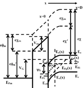
A schematic diagram of the n-type silicon MOS-TD op-erated in strong accumulation is shown in Fig. 1. A p-type MOS-TD is similar, but the applied voltage VGhas opposite polarity. Voxis the voltage drop across the oxide barrier,Sis the voltage drop across the silicon substrate 共or band bend-ing兲,mis the work function of the metal, is the electron affinity of silicon, andox is the electron affinity of the ox-ide. The band bending at the back electrode is共D兲=0, and at the Si/ SiO2 interface it is defined as共0兲=S. The con-duction band and the valence band energies inside the sub-strate are given as Ecand Ev, respectively. The two energies vary across the substrate and are given as Ec共x兲=Ec−共x兲 and Ev共x兲=Ev−共x兲, respectively. At the Si/SiO2 interface, they are written as Ec
0and Ev0. The quasi-Fermi level of the interface states is EFt. The applied voltage can be obtained from the following equations:
VG=ms+ Vox+S, 共5兲
ms=m
⬘
−⬘
−冉
Eg2e−Fn
冊
, 共6兲whereFn=关EFn共D兲−Ev− Eg/ 2兴.
The voltage drop across the oxide is given by Vox=
tox ox
关QS共S兲 + Qit+ QX兴, 共7兲
where toxis the oxide thickness andoxis the corresponding dielectric constant. The surface charge density of the
semi-FIG. 1. Energy bands of a metal-insulator-semiconductor silicon tunneling diode.
conductor, QS共C cm−2兲, is given by QS共S兲=兩S共d/ dx兲兩x=0. The fixed charge density in the oxide, QX共C cm−2兲, is related to the fixed charge density NX 共cm−2兲 by QX= eNX. The in-terface charge density Qit 共C cm−2兲 is written as Qit = eDit共EFn− EFt兲, where the interface-state density function Dit 共cm−2eV−1兲 is assumed to be uniform across the silicon band gap.
To determine the surface band bending S, the Poisson equation is solved numerically:15
2
x2共x兲 = − e
S共p − n + ND兲, 共8兲
where NDis the doping concentration of the silicon substrate andS is the dielectric constant of silicon.
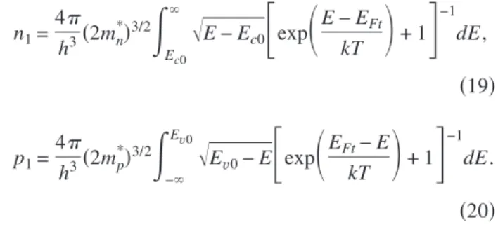
Various current density components in a n-type MOS-TD are shown in Fig. 2. J is the total current density flowing from the metal electrode to the silicon back elec-trode, Jnt is the tunneling current density to the conduction band, Jptis the tunneling current density to the valence band, JSS is the tunneling current density to Si/ SiO2 interface states, Jnsis the recombination current density from the con-duction band to the interface states, Jpsis the recombination current density from the valence band to the interface states, Jn is the drift current density of electrons, and Jpis the dif-fusion current density of holes.
The node equations include Eq. 共9兲 at the metal electrode/back electrode, Eq.共10兲 at the interface states, Eq. 共11兲 at the conduction band, and Eq. 共12兲 at the valence band:
J = Jnt+ Jpt+ JSS= Jn+ Jp, 共9兲
JSS= Jns− Jps, 共10兲
Jnt= Jn− Jns, 共11兲
Jpt= Jp+ Jps. 共12兲
On combining Eqs. 共9兲–共12兲, Eq. 共13兲 is obtained, which is used to calculate the total current density J at different ap-plied voltages Vg from Jnt, JSS, Jps, and Jp,
J = Jnt+ JSS+ Jps+ Jp. 共13兲
The tunneling current densities from the metal electrode to the conduction band and to the valence band, Jntand Jpt, respectively, are given in Ref. 10 and rewritten here as Eqs. 共14兲 and 共15兲, without employing the Maxwell-Boltzmann approximation of the occupation probability. The energy dif-ference of each term in Eqs.共14兲 and 共15兲 is Ec共0兲−EFn共0兲 = Ec+ eS− EFn, Ec共0兲−EFm= eVox− e共m
⬘
−⬘
兲, EFm− Ev共0兲 = Eg− eVox+ e共m⬘
−s⬘
兲, and EFp共0兲−Ev共0兲=EFp共0兲−共Ev + eS兲, respectively. When the n-type MOS-TD is operated in strong accumulation, the quasi-Fermi level of electrons at the silicon surface, EFn共0兲, is normally above the metal Fermi level EFm, as the voltage drop across the oxide is positive. Therefore the electron tunneling current is from the metal electrode to the conduction band. The quasi-Fermi level of holes EFpis also well above the metal Fermi level EFmeven if it is lower than EFn. Thus the tunneling current of holes flows from the metal electrode to the valence band. The tunneling barrier height of electrons n and holespis assumed to be 0.7 eV.12The unit used for oxide thickness tox is angstrom, for brief formulation.10The transverse effective mass mtis taken to be the same as mn* and mp
*
for the corre-sponding current density:
Jnt= emt ប3exp共−
冑
ntox兲冕
0 ⬁冉
再
exp冋
E + Ec共0兲 − EFn共0兲 kT册
+ 1冎
−1 −再
exp冋
E + Ec共0兲 − EFm kT册
+ 1冎
−1冊
EdE, 共14兲 Jpt= emt ប3 exp共−冑
ptox兲冕
0 ⬁冉
再
exp冋
EFm− Ev共0兲 + E kT册
+ 1冎
−1 −再
exp冋
EFp共0兲 − Ev共0兲 + E kT册
+ 1冎
−1冊
EdE. 共15兲 To treat the current densities related to the interface states11without an approximation of the occupation probabil-ity, JSS, Jns, and Jpsare derived as shown below:JSS=
冕
Ev Ec eDit t 共ft− fm兲dE = eNit tEg冕
0 Eg冉
再
exp冋
E + Ev共0兲 − EFt kT册
+ 1冎
−1 −再
exp冋
E + Ev共0兲 − EFm kT册
+ 1冎
−1冊
dE, 共16兲 Jns= eNitvthn关共1 − ft兲nS− ftn1兴, 共17兲 Jps= eNitvthp关ftpS−共1 − ft兲p1兴, 共18兲 wherevthis the thermal velocity, n andp are the capture cross sections of electrons and holes by the interface states, and t is the tunneling time constant of electrons from the metal electrode to the interface states. nS= n共x=0兲 and pSFIG. 2. Current density components of a metal-insulator-semiconductor tun-neling diode in strong accumulation.
= p共x=0兲 are the surface concentrations of electrons and holes, respectively. n1 and p1 are expressed as
n1= 4 h3共2mn *兲3/2
冕
Ec0 ⬁冑
E − Ec0冋
exp冉
E − EFt kT冊
+ 1册
−1 dE, 共19兲 p1=4 h3共2mp *兲3/2冕
−⬁ Ev0冑
Ev0− E冋
exp冉
EFt− E kT冊
+ 1册
−1 dE. 共20兲 The interface-state density function Dit 共cm−2eV−1兲 is as-sumed to be uniformly distributed over the band gap, so the total interface-state density is given by Nit= DitEg 共cm−2兲. The occupation probability ft can be determined from Eqs. 共10兲 and 共16兲–共18兲. Then EFtis retrieved fromft= Eg−1
冕
0 Eg关exp共E + Ev− EFt兲 + 1兴−1dE. 共21兲 The device is in quasiequilibrium, so the majority carrier concentration n共x兲 and the minority carrier concentration p共x兲 are determined by the quasi-Fermi levels in Eqs. 共1兲 and 共2兲. The value of EFn共x兲can be determined from the majority drift current density by Jn=nn共dEFn/dx兲. A small amount of variation in the quasi-Fermi level of the majority carriers can result in a large current flowing through the bulk region due to the large majority carrier concentration in strong accumulation.10To a good approximation, it can be assumed that EFnremains constant throughout the bulk region and the majority carrier concentration n共x兲 does not differ greatly from the value in thermal equilibrium n¯共x兲.
The minority carrier concentration p共x兲=p¯共x兲+⌬p共x兲 as well as EFp共x兲 can be determined from the ambipolar carrier transport equation, or the diffusion equation
Dp d2
dx2p + g¯ − R = dp
dt = 0, 共22兲
where Dp is the diffusion coefficient in the n-type silicon substrate. The hole concentration p共x兲 is many orders larger than its thermal equilibrium value p¯共x兲 when the diffusion current flows to the accumulation region. The generation rate per volume density in thermal equilibrium g¯ is given by
g
¯ = Bn¯ p¯ + A共n¯ + p¯兲. 共23兲
The product Bn¯ p¯ still gives a good approximation to the radiative recombination rate in thermal equilibrium in a MOS junction without the tunneling current. A共n¯+p¯兲 is the nonradiative recombination rate per unit volume by bulk traps and is expressed as11
A共n¯ + p¯兲 =Nbtvth共n¯ +n p¯p兲
bt
, 共24兲
where Nbtis the bulk-trap density共cm−2兲 andbtis the bulk-trap time constant. The recombination rate R in quasiequilib-rium is expressed as Eq. 共3兲. Through combining Eqs. 共3兲 and共22兲–共24兲, the diffusion equation 共22兲 becomes Eq. 共25兲.
The diffusion current density of the minority carrier Jp is defined as Dp d2 dx2共⌬p兲 − 关Bn¯共⌬p兲 + A共⌬p兲兴 = 0, 共25兲 Jp= − eDp
冏
d dx共⌬p兲冏
x=0= − e冕
0 H 关Bn¯共⌬p兲 + A共⌬p兲兴dx. 共26兲 Jp in Eq. 共26兲 can be written as the integral form if the radiative recombination-generation current density is defined as Jrg= e兰0xBn¯共⌬p兲dx and the nonradiative recombination cur-rent density from bulk traps is defined as Jbt= e兰0xA共⌬p兲dx. The diffusion equation 共26兲 is then readily written as Eq. 共27兲. The current densities Jp, Jrg, and Jbt are used to deter-mine the internal carrier recombination efficiency and the carrier recombination lifetime,Jp= Jrg+ Jbt= e
冕
0 H Bn¯共⌬p兲dx + e冕
0 H A共⌬p兲dx. 共27兲To obtain the relation of the total current density through the device J to the given applied voltage VG, the quasi-Fermi level of the majority carriers EFn, for example, electrons in a n-type MOS-TD, is assumed to be constant within silicon. The variation of the electron concentration is calculated by the band bending function 共x兲. To reach a consistent solu-tion, the algorithm is described in the following steps: 共a兲 Quasi-Fermi level of holes is the same as that of
elec-trons EFp共x兲=EFn共x兲 and ⌬p共x兲=0.
共b兲 Surface band bending s is obtained by solving the Poisson equation, Eq.共8兲.
共c兲 Balance equation for Jns, Jps, and JSS in Eq. 共10兲 is solved to give EFt.
共d兲 Diffusion equation for holes in Eq. 共27兲 is solved to give⌬p and Jp.
共e兲 If 兩Jpt− Jps− Jp兩⬍tolerance, then J is given by Eq. 共9兲. Otherwise it repeats from 共b兲 to 共d兲, with p共x兲=p¯共x兲 +⌬p共x兲.
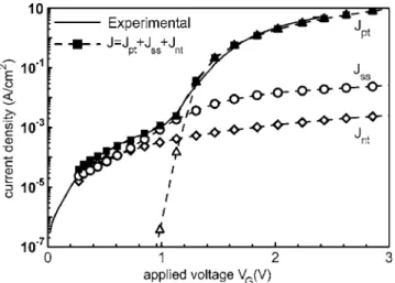
Figure 3 shows both the experimental J-V curve from a fabricated n-type MOS-TD device 共solid line兲 and the theo-retical curves 共dotted line兲 obtained from the above algo-rithm. The total current density J is the sum of the tunneling current density to the majority band Jnt in Eq. 共14兲, to the minority band Jpt in Eq.共15兲, and to the interface states JSS in Eq.共16兲. The kink of the J-V curve at the applied voltage of 1.0 V indicates that the tunneling current density to the valence band Jpt raises orders of magnitudes larger than the current density to the conduction band Jnt and the interface states JSS. Therefore, Jptis the major part of the total tunnel-ing current density in a n-type MOS-TD operated in strong accumulation. The same situation happens to the p-type MOS-TD in forward bias, where Jntis the major part of the total tunneling current density.11 However, this does not mean that most tunneling current density becomes the minor-ity diffusion current densminor-ity Jp. Only part of Jptbecomes the diffusion current density and contributes to radiative
recom-bination. Another part becomes the recombination current density Jpsthrough the interface states. This is because ftin Eq.共18兲 is pinned near the conduction band edge for a very low fmin strong accumulation.
The surface band bending and the oxide voltage drop with respect to different applied voltages are shown in Fig. 4. The interpretation is as follows: at an applied voltage of higher than 0.2 V in the n-type MOS-TD, the voltage almost falls on the oxide as shown, so Voxchanges linearly with VG. The voltage drop across the region of the semiconductor band bending is only a few hundred meV. This voltage drop cannot increase much more. When the quasi-Fermi level of electrons is above the conduction-band edge, the band bend-ing and the electron concentration do not increase signifi-cantly with applied voltage.
The surface concentrations of electrons are depicted in Fig. 5. The value of the surface concentration of electrons ns reaches 2⫻1019cm−3 when the quasi-Fermi level of elec-trons EFn is lifted above Ec, for the applied voltage of less than 1 V. The value of the surface concentration of holes ps also approaches 7⫻1018cm−3, when the quasi-Fermi level
of holes EFpreaches Evand the applied voltage exceeds 2 V. The minority tunneling current density Jpthas a larger mag-nitude than the other two tunneling current densities, Jntand JSS, as shown in Fig. 3. To dissipate such a large current, the surface concentration of holes is raised. In such a case, the strong accumulation of both electrons and holes leads to an intense radiative recombination rate at the semiconductor surface.
III. LIGHT CONVERSION EFFICIENCY AND ITS IMPROVEMENT
After the carrier concentrations and all current densities are formulated at the given applied voltage, light emission efficiency is then derived from the model in Sec. II. The externally detected photon emission flux L /ប共cm−2兲 of the MOS-TD operated as a light emitter is expressed as follows: L/ប=c共JrgSA/e兲 =ci共JSA/e兲, 共28兲 where Jrgis the recombination current density,cis the light extraction efficiency from a MOS-TD light emitter to a pho-todetector,iis the internal quantum efficiency, and SAis the total area of injection current. The external quantum effi-ciency is expressed as ext=
冉
e ប冊冉
L JSA冊
=ci. 共29兲The injection efficiency inj can be obtained from Eq. 共13兲 and written as
inj=
Jp Jnt+ JSS+ Jps+ Jp
. 共30兲
The internal bulk recombination efficiency rec can be ob-tained from Eq.共27兲 and explicitly expressed as
FIG. 3. Comparison of the tunneling current density vs voltage relation of a
n-type MOS-TD共solid line兲 and the fitted simulation curves of the tunneling
current density共tox= 1.5 nm兲. The total current density J 共square dotted兲 is
the sum of tunneling current densities to the minority band Jpt 共triangle
dotted兲, to the majority band Jnt共diamond dotted兲, and to the interface states
JSS共circle dotted兲.
FIG. 4. Simulation of the surface band bending and the oxide voltage drop of a n-type MOS-TD共tox= 1.5 nm兲.
FIG. 5. Simulation of the surface carrier concentration of electrons in a
n-type MOS-TD with respect to different current densities in the
rec= Jrg Jrg+ Jbt = e
冕
0 H Bn¯共⌬p兲dx e冕
0 H Bn¯共⌬p兲dx + e冕
0 H A共⌬p兲dx . 共31兲Combining Eqs. 共30兲 and 共31兲, the internal quantum effi-ciency becomesi=recinj.
To improve external quantum efficiency, one may in-crease the light extraction efficiencycby applying an anti-reflection pattern to the Si surface,4 increase the injection efficiency by reducing the interface states, or increase the recombination efficiency by reducing the bulk traps. In the modern IC industry, the silicon wafer has a high crystal qual-ity that results in a carrier lifetime as high as several milli-seconds. However, the interface-state density can only be reduced to the order of 1010cm−2. The tunneling current den-sity to the valence band Jpt consists of the recombination current density to the interface state Jps and the diffusion current density Jp. The portion of the diffusion current den-sity contributed by Jptis simulated to be several tens of per-cents according to different interface-state densities. There-fore, the internal recombination efficiency iin bulk silicon is estimated to be a few tens of percents. This estimation can be also deduced from the small-signal light-current response and is discussed in Sec. IV. The light extraction efficiency, however, can be very low if the generated light is blocked by the thick metal pad. The external quantum efficiency from the periphery of the metal pad is around 10−4 in the SiO2 nanoparticle-modified MOS-TD.2
The arguments about injection efficiency also predict an-other possibility of raising the external quantum efficiency. If the radiative recombination coefficient B is raised by the benefit of a carrier confinement structure, the diffusion cur-rent density will be enhanced due to the fast dissipation of the injected current. The injection efficiency can then be fur-ther increased without facing the difficulty of reducing the interface-state density.
IV. SMALL-SIGNAL LIGHT-CURRENT RESPONSE
To further broaden the carrier dynamic model, the small-signal response of light emission by a modulation current is investigated. A strong influence of the injection current den-sity on the response time, or the carrier lifetime, is found in the MOS-TD. This effect exists in the rapid-thermal-oxide MOS-TD at a very high injection current density and is mea-surable at a lower injection current density in the SiO2 nanoparticle-modified MOS-TD.16 In discussions of this ef-fect, the frequency response of the current with respect to the voltage modulation in a MOS junction, or the small-signal capacitance-voltage 共CV兲 method, is reviewed. It is a com-mon technique used to characterize the influence of the in-terface states on electrical performance, and has been ex-tended to the MOS tunneling diode, which involves the tunneling current to the conduction band, the valence band, and the interface states.11The response time of the current by small-signal voltage modulation is limited by the majority tunneling current density Jnt, the tunneling current density to interface states JSS, and the minority tunneling current
den-sity Jpt. The time constant CV can be expressed as in Eq. 共32兲, where GCBand GVBare the tunneling conductances of the tunneling currents to the conduction band and the valence band, respectively, Gp and Cp are the conductance and ca-pacitance of the recombination current to interface states, respectively, GTis the conductance of the tunneling current to interface states, CSCis the capacitance due to the surface charge, and Coxis the oxide capacitance. The typical value of
CVis lower than 1s in the MOS-TD with an active area of 0.01 cm2,
CV −1
= 2关Cox/共GT+ GCB+ GVB兲 + 共Cox+ CSC+ CP兲/Gp兴. 共32兲 The small-signal response of light with respect to the modulation current is considered here because the MOS-TD is now operating as a light emitter. The small-signal light-current response is normally around 10– 100s, slower than
CV. From Eqs.共30兲 and 共31兲, the modulation speed of light generation with respect to the different current densities is mainly controlled by two factors: the nonradiative recombi-nation rate through the interface states and the recombirecombi-nation rate in the bulk region. Therefore, the response of light emis-sion to the small-signal current modulation, i.e., the ratio of the modulated light amplitude to the modulated current am-plitude, is expressed as L共i兲 JSA =ប e EQE 1 1 + iL , 共33兲
where the response time L is expressed as L −1
=0−1+rec−1. EQE is the external quantum efficiency under DC bias. The response time can be derived from the light-current amplitude-frequency plot by the frequency response mea-surement and is explained later. The parameter rec is the response time of the diffusion equation 共27兲. The parameter
0=共2Cp/ Gp兲−1 is the response time of the recombination current density through interface states JSS and Jps. Capaci-tance Cpand conductance Gp are frequency dependent; they vary significantly with the surface concentration of the ma-jority carriers when the applied frequency is approaching the inverse of interface recombination times⬇共nsvthn兲−1.12In the small-signal light-current response of the MOS-TD, be-cause the operation frequency of the modulation current is much less thans,0 can be assumed to be independent of the total injection current density J.
In the small-signal capacitance-voltage response, the interface-state conductance共Gp兲 of a MOS-TD, even acting as a light emitter, is less influential than the direct tunneling conductance in accumulation.17However, in the small-signal light-current response, its contribution to the response time of light generation is not negligible. This is because the re-sponse time of light generation is mainly limited by both radiative and nonradiative recombination rates, not the cur-rent injection rate. The response time is a few tens of micro-seconds and the nonradiative recombination time0, involv-ing Gp, is a few hundreds of microseconds. In such a case, to better estimate the radiative recombination lifetime,0must be included. Therefore, Gp is considered here.
The variation of light emission response time with the different bias current densities is mostly related to the recom-bination timerecin the bulk region.The response timeLis explicitly expressed in the following equation:
L−1=0−1+rec−1=0−1+
冕
0 H 关共Bn¯ + A兲␦⌬p兴dx冕
0 H ␦⌬pdx ⬇0 −1 +共Bn¯ + A兲Ln Lp . 共34兲The parameter Lnis the accumulation depth of electrons. It is defined as the distance from the surface to the point where the electron concentration reduces to 1%. Its value is around 0.3 nm when the injection current is several A / cm2. The parameter Lpis the accumulation depth of holes. It is defined as the distance from the surface to the point where the hole concentration reduces to 1%. Its value is around 5 nm, ac-cording to the solution of Eq. 共27兲. The product Ln/ Lp is proportional to the concentration of the excess minority car-riers ⌬p, as the higher ⌬p results in higher recombination rate in the bulk region when the device is operated in strong accumulation.
The internal efficiencyi=recinjcan also be analyzed from Eqs. 共30兲, 共31兲, and 共34兲. It is expressed as i =rec−1/共0−1+rec−1兲. To estimate the value of the nonradiative recombination coefficient A, the optically pumped carrier lifetime is measured by laser-excitation microwave photo-conductivity decay共MW-PCD兲 of the silicon wafer in 0.8 M iodine/ethanol.18 The laser excitation creates a lower injec-tion level, compared with electrical injecinjec-tion. The excess car-rier concentration nPCD is in the range of 1016– 1017cm−3. The float-zone growth Si wafer used has a MW-PCD lifetime of 1 – 3 ms. The internal photoluminescent共PL兲 efficiency is estimated to be 10% with the consideration of a lifetime of 30 ms in the purest wafers.19 In such a case, the internal efficiency is modified to
PCD⬇ mBn¯s mBn¯s+ A
, 共35兲
where m is the ratio of nPCDto the surface concentration of electrons nsin a normally operated MOS-TD. Supposed the laser-pumped excess electron concentration is 1016cm−3, then the value of A is estimated to be 270 s−1 in a sample with a 3 ms MW-PCD lifetime. This means that in the nor-mal operation of a MOS-TD, the internal EL efficiency in bulk silicon is nearly 100%. In comparison, the light emis-sion efficiency is only several percent below the usual PL or MW-PCD measurement. The high internal EL efficiency is due to the large carrier concentration at the surface when the MOS-TD is operated in strong accumulation.
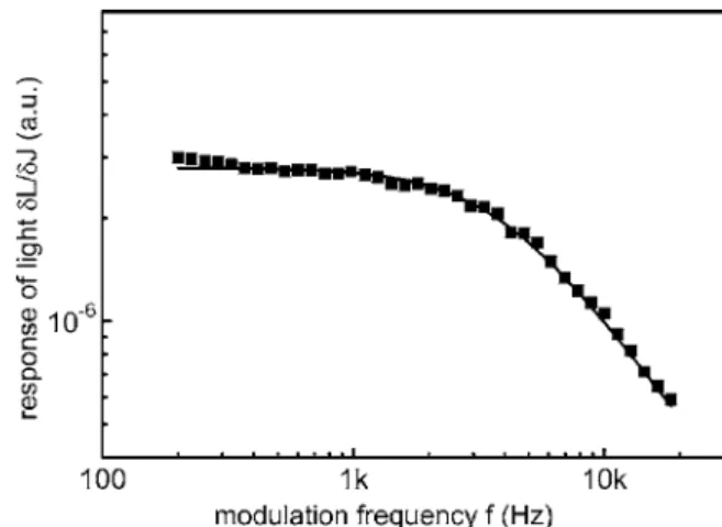
Frequency response is used to measure the light-generation response time, as the response of the output light in Eq. 共33兲 and the response time in Eq. 共34兲 give informa-tion on the radiative and nonradiative recombinainforma-tion rates. This method shows how the carrier lifetime changes with different bias current densities. Its principle is to modulate
the biased light-emitting MOS-TD with a small-signal sinu-soidal current. The measurement setup of frequency response is illustrated in Fig. 6. The modulation source 共Agilent 33210A兲 is fed to the device under a dc bias. The dc bias is provided by Keithley 2400. After the voltage excitation is applied to the EL MOS-TD, the current is measured through a 1 ⍀ resistance. The modulation amplitude of the current density ␦J is maintained at 0.5 A / cm2 over all bias current densities. The modulated light amplitude ␦L is detected by an InGaAs detector with a response time smaller than 100 ns and extracted from the output light through a lock-in ampli-fier共Stanford Research Systems SR830兲. The modulated cur-rent density ␦J is detected by another lock-in amplifier.
Figure 7 shows how the modulated output light ampli-tude decreases as the modulation frequency increases in a n-type MOS-TD. The response of light, i.e., the ratio of the modulated light amplitude␦L to the modulated current den-sity amplitude␦J, is proportional to 1 /
冑
1 +共2fL兲2 accord-ing to Eq.共33兲, where f is the modulation frequency andL is the response time. The response time L can be derived from the curve fitting of the response of light in Fig. 7.The tunneling current density significantly affects the majority carrier density as well as the carrier lifetime. In the previous measurement of temporal response,8,9 the input modulation is a current pulse that varies from zero to a large value. As the carrier lifetime strongly varies with the differ-ent currdiffer-ent levels, the dependence of lifetime on the currdiffer-ent density might not be simply extracted. In the frequency re-sponse measurement here, the modulation current density is only a few percent of the bias current density. Therefore the
FIG. 6. The measurement setup of the small-signal light-current response of EL MOS-TDs.
FIG. 7. The response of light, i.e., the ratio of the modulated light amplitude ␦L to the modulated current density amplitude ␦J, of a n-type silicon
modulation has less effect on the lifetime, i.e., the response time. As a result, this method shows more clearly how the response time is related to the bias current density as well as the majority carrier density.
The minority carrier lifetime is influenced by the radia-tive recombination of electrons and holes and nonradiaradia-tive recombination through bulk traps and interface states. With a high level current density larger than 1 A / cm2, it is operated in strong accumulation and the quasi-Fermi level EFn is above the conduction band edge. A further injection of elec-trons increases the surface concentration of elecelec-trons slowly by raising EFn. From Fig. 5, the surface concentration of electrons ns can be approached by the relation ns= 0.55 + 0.65J1/2, where nsis in units of 1020cm−3and J is in units of A / cm2. Moreover, at this level of current density, the nonradiative recombination rate through interface states does not increase further, as the quasi-Fermi level of the interface states remains the same in strong accumulation.
Figure 8 shows the relation between response time and the bias current density of two n-type MOS-TDs. Devices A and B are both SiO2 nanoparticle-modified MOS-TDs, fab-ricated by spin coating a 120 nm thick layer of oxide nano-particles onto Si. The particle size is 8 – 10 nm. The wafer is treated with KOH solution prior to the spin coating of oxide nanoparticles to remove the polish damage.2 Both devices have a metal pad area of 0.01 cm2. The external light emis-sion efficiencyextis 10−5and 5⫻10−6共W/A兲 for A and B, respectively. To fit the response time curve in Fig. 8, the radiative recombination coefficient is needed. In EL MOS-TDs, the physical mechanism of light emission is phonon-assisted radiative recombination of electrons and holes in bulk silicon. This recombination mechanism is the same as the photoluminescence in bulk silicon in Ref. 20, so the re-ported value of B = 2⫻10−15cm3/ s can be used. The data fitted are t0= 364s, Ln / Lp = 0.06 for device A and t0 = 124s, Ln / Lp = 0.04 for device B. The higher value of t0 in device A corresponds to a lower interface-state density Nit, so the light emission efficiency of device A is higher than that of device B. When the device has a lower interface-state density, it also has a larger surface concentration of holes, and thus a higher Ln / Lp value, according to Eq. 共34兲. The
theoretical internal efficiency 共i兲 can be calculated to be 90% and 72% for devices A and B, respectively. Other fac-tors such as the leak current through oxide pores may reduce the injection efficiency and is not measurable in the small-signal light-current response.
V. CONCLUSION
This work derives in detail the carrier dynamic model of metal-oxide-semiconductor silicon tunneling diodes. The model satisfactorily explains the current-voltage characteris-tics, light emission efficiency, and the dependence of the small-signal light-current response time on the bias current density. A large majority carrier concentration is accumulated at the semiconductor surface in strong accumulation. The tunneling current density to the minority band is found to be much larger than the tunneling current densities to the ma-jority band and the interface states. Part of the minority tun-neling current density becomes the diffusion current and most of the diffusion current produces light by radiative re-combination in the bulk region. Several percent of the mi-nority tunneling current density recombine nonradiatively through the interface states. The internal efficiency is mainly determined by the interface-state density and also influenced by the bulk-trap density.
Information on interface states can be retrieved from the small-signal light-current plot versus the injection current density. The result is explained by the relation of the surface carrier concentration with respect to the injection current density. The device with a higher initial response time has lower interface states and thus higher light emission effi-ciency. The relation of the surface majority carrier concen-tration with the injection current density is modeled. It is used to explain the small-signal light-current response. The theoretical internal efficiency is estimated to be several tens of percents from the extracted interface-state response time.
ACKNOWLEDGMENTS
The authors wish to acknowledge the support of the Na-tional Science Council under Contract Nos. NSC 94-2120-M-002-010 and NSC 94-2622-E-002-005. The authors would also like to thank the Nissan Chemical America Cor-poration for the supply of SiO2nanoparticles.
1C. W. Liu, M. H. Lee, M. J. Chen, I. C. Lin, and C. F. Lin, Appl. Phys.
Lett. 72, 1516共2000兲.
2C. F. Lin, P. F. Chung, M. J. Chen, and W. F. Su, Opt. Lett. 27, 713
共2002兲.
3W. L. Ng, M. A. Lourenco, R. M. Gwilliam, S. Ledain, G. Shao, and K. P.
Homewood, Nature共London兲 410, 192 共2001兲.
4M. A. Green, J. Zhao, A. Wang, P. J. Reece, and M. Gal, Nature共London兲 412, 805共2001兲.
5M. H. Lee, K. F. Chen, C. C. Lai, C. W. Liu, W. W. Pai, M. J. Chen, and
C. F. Lin, Jpn. J. Appl. Phys., Part 2 41, L326共2002兲.
6C. F. Lin, T. W. Su, P. F. Chung, E. Z. Liang, M. J. Chen, and C. W. Liu,
Mater. Chem. Phys. 77, 430共2002兲.
7M. J. Chen, E. Z. Liang, S. W. Chang, and C. F. Lin, J. Appl. Phys. 90,
789共2001兲.
8M. J. Chen, C. F. Lin, M. H. Lee, and S. T. Chang, Appl. Phys. Lett. 79,
2264共2001兲.
9M. J. Chen, J. F. Chang, J. L. Yen, C. S. Tsai, E. Z. Liang, C. F. Lin, and
C. W. Liu, J. Appl. Phys. 93, 4253共2003兲.
10H. C. Card and E. H. Rhoderick, J. Phys. D 4, 1602共1971兲.
FIG. 8. The small-signal light-current response times with respect to differ-ent bias currdiffer-ent densities 共triangle, device A; square, device B兲 and the simulation curves共solid兲.
11L. R. Freeman and W. E. Dahlke, Solid-State Electron. 13, 1483共1970兲. 12M. Y. Doghish and F. D. Ho, IEEE Trans. Electron Devices 39, 2771
共1992兲.
13C. D. Thurmond, J. Electrochem. Soc. 122, 1133共1975兲.
14V. Alex, S. Finkbeiner, and J. Weber, J. Appl. Phys. 79, 6943共1996兲. 15J. Sune, P. Olivo, and B. Ricco, J. Appl. Phys. 70, 337共1991兲. 16C. F. Lin, T. W. Su, E. Z. Liang, H. H. Hsieh, and W. P. Huang, Proc. SPIE
4996, 4996–07共2003兲.
17E. Nicollian, A. Goetzberger, and A. Lopez, Solid-State Electron. 12, 937
共1969兲.
18E. Yablonovitch, D. L. Allara, C. C. Chang, T. Gmitter, and T. B. Bright,
Phys. Rev. Lett. 57, 249共1986兲.
19A. W. Stephens and M. A. Green, Sol. Energy Mater. Sol. Cells 45, 255
共1997兲.
20G. Augustine and A. Rohatgi, IEEE Trans. Electron Devices 39, 2395