奈米點非揮發性記憶體元件之研究
71
0
0
全文
(2) 本論文獻給我摯愛的父母 林添壽先生 林陳鳳珠女士.
(3) 奈米點非揮發性記憶體元件之研究 Study on Nanocrystal Nonvolatile Memory Devices 研 究 生:林泩宏 指導教授:施 敏 博士 張鼎張 博士. Student : Sheng Hung Lin Advisor : Dr. Simon M. Sze Dr. Ting-Chang Chang. 國 立 交 通 大 學 電子工程學系. 電子研究所碩士班. 碩 士 論 文 A Thesis Submitted to Institute of Electronics College of Electrical Engineering and Computer Science National Chiao Tung University in Partial Fulfillment of the Requirements for the Degree of Master of Science in Electronic Engineering June 2004 Hsinchu, Taiwan, Republic of China. 中華民國 九十三 年 六 月.
(4) 奈米點非揮發性記憶體元件之研究. 研 究 生: 林泩宏. 指導教授: 施. 敏 博士. 張 鼎 張 博士. 國 立 交 通 大 學 電子工程學系 電子研究所. 摘要. 傳統的非揮發性記憶體是利用複晶矽浮停閘(floating gate)做為載子儲存的 單元,當浮停閘儲存由通道注入的電子之後,元件的起始電壓就會發生改變,利用 起始電壓的差異作為記憶體 0 和 1 邏輯的定義。然而,由於浮停閘是連續的一層 半導體薄膜,在反覆的操作下,一旦穿隧氧化層(tunnel oxide)出現漏電路徑,儲存 的電荷就會全部流失,記憶體就會失效,因此穿隧氧化層的厚度無法縮減下來,操 作電壓無法降低,速度也無法增快。一般認為當元件通道長度達到 65 nm 時,便是 此種結構的極限。本研究利用半導體或金屬奈米點作為電荷儲存的單元,可以減 少穿隧氧化層的厚度,而不損失可靠性,進而降低操作電壓,並使元件縮小密度提 高,操作速度增快。 利用半導體或金屬奈米點作為電荷儲存的單元。在元件的反覆操作下,即使 穿隧氧化層產生缺陷或漏電路徑,所損失掉的儲存電子,僅是單一奈米點的電子漏 失,對整體元件特性的影響並不明顯。因此,穿隧氧化層的厚度得以縮減,使得操 i.
(5) 作速度提升,元件積集度增加,元件可操作的次數(endurance)以及保存時間 (retention)也同時得到改善。當電子儲存在奈米點時,由於庫倫阻絕(Coulomb blockade)效應,儲存的電子會限制後續電子的注入。奈米點的庫倫阻絕效應使得 記憶體元件的儲存及操作更加的穩健。當閘極偏壓使通道產生反轉層後,通道的 電子藉由直接穿隧效應或是 F-N 穿隧效應通過穿隧氧化層,而讓奈米點捕獲,是為 寫入動作。當閘極偏壓反向時,儲存的電子便經由穿隧氧化層回到通道,是為抹除 動作。藉由電容-電壓(C-V)量測,當電子注入奈米點之後,元件之起始電壓會發生 偏移,此偏移的量即定義為記憶體元件的記憶窗。 本研究提出於穿隧氧化層上利用低壓化學氣相沈積(LPCVD)成長 SiGe 薄膜, 並以熱氧化方式,使矽氧化成為二氧化矽作為控制氧化層,而鍺元素向下析出在 穿隧氧化層上,作為載子儲存的單元。由穿透式電子顯微鏡圖(TEM)知,鍺奈米點 析出於穿隧氧化層上,穿隧氧化層厚度約 4.5 奈米,鍺奈米點的尺寸大約 5.5 奈米, 經由電性計算密度大約為 4.2*1011/cm2。由圖中可估算,在 5 伏的操作電壓下,記憶 窗大約有 0.42 伏,足夠作為記憶體定義 0 與 1。然而當增加 SiGe 薄膜熱氧化時間, 鍺便會氧化為氧化鍺,形成氧化鍺奈米點。經由電性量測後發現,氧化鍺奈米點 也確實有記憶體特性,另外經由 x-ray absorption near edge spectroscopy (XANES) 也證實穿透式電子顯微鏡照片中的奈米點成分為氧化鍺,我們並且提出了一個物 理模型來解釋此元件之記憶體效應。另外,在金屬奈米點方面,我們提出利用鉑金 屬濺鍍於穿隧氧化層上,不需經過熱處理,自我組裝成核,鉑(Pt)奈米點的製作方 式,藉由製程上的改進,可形成金屬奈米點並得到金屬奈米點的記憶體特性,並且 在 5 伏的操作電壓下,達到 0.25 伏的起始電壓偏移(記憶窗) 。. ii.
(6) Study on Nanocrystal Nonvolatile Memory Devices. Student: Sheng Hung Lin. Advisor: Dr. Simon M. Sze Dr. Ting-Chang Chang. Department of Electronic Engineering and Institute of Electronics College of Electrical Engineering and Computer Science National Chiao Tung University. Abstract. In a conventional nonvolatile memory, charge is stored in a polysilicon floating gate (FG) surrounded by dielectrics. The scaling limitation stems from the requirement of very thin tunnel oxide layer. For FG, once the tunnel oxide develops a leaky path under repeated write/erase operation, all the stored charge will be lost. Therefore, the thickness of the tunnel oxide can not be scaled down to about 7 nm. To alleviate the scaling limitation of the conventional FG device while preserving the fundamental operating principle of the memory, we have studied the distributed charge storage approach such as the nanocrystal nonvolatile memory. Each nanodot will typically store only a handful of electrons; collectively the charges stored in these dots control the channel conductivity of the memory device. Nanocrystal charge storage offers several advantages, the main one being the potential to use thinner tunnel oxide without sacrificing nonvolatility. This is a quite attractive proposition since reducing the tunnel oxide thickness is a key to lowering operating. iii.
(7) voltages and/or increasing operating speeds. The improved scalability results not only from the distributed nature of the charge storage, which makes the storage more robust and fault-tolerant, but also from the beneficial effects of Coulomb blockade. A local leaky path will not cause a fatal loss of information for the nanocrystal nonvolatile memory device. Also, the nanocrystal memory device can maintain good retention characteristics and lower the power consumption. We have fabricated a nonvolatile memory device embedded with Ge nanocrystals by a thermal oxidation of Si0.8Ge0.2 combined with a rapid thermal annealing process. The tunnel oxide in the nonvolatile memory is 4.5 nm-thick and with 5.5-nm Ge nanocrystals reside on it. A low operating voltage, 5V, is implemented and a significant threshold-voltage shift, 0.42V, is observed. Also, we have demonstrated the novel distributed charge storage with GeO2 nano-dots. The mean size and aerial density of the dots are estimated to be about 5.5 nm and 4.3×1011 cm-2, respectively. The composition of the GeO2 dots is confirmed by the XANES measurements. In electrical analyses, a significant memory effect is observed with a threshold voltage shift of 0.45V under 5-V operation. Also, a physical model is proposed to explain the charge storage via the interfacial traps of GeO2 nano-dots. We have also proposed a simple process to fabricate metal nanocrystal memory which is one of the candidates that have great potential of achieving fast write/erase and long retention time simultaneously. Once the self-assembled nanocrystals have controllable density and size distribution, the metal nanocrystals can be incorporated into a standard MOSFET structure to fabricate nonvolatile memory devices.. iv.
(8) 誌謝 兩年的碩士生涯, 眨眼間已到了鳳凰花開, 依依不捨的畢業時刻。 在畢業典 禮的會場, 跟著大家一起拍照留念, 互道珍重再見, 為彼此的相遇留下歷史的見 證, 而典禮結束時的煙火, 在漆黑的夜空閃閃發亮, 也代表了對畢業生的祝福, 不管在這些時間背後的快樂悲傷, 喜悅心酸。 ㄧ路走來, 首先我要感謝的是我的兩位指導教授施敏教授與張鼎張教授。 做研究時, 施敏教授的指導與教悔令學生猶如在茫茫學海做出正確的指引, 與施 教授的言談中更可顯出老師的睿智以及對學生的啟發, ㄧ代巨擘風範表露無遺 在其溫文儒雅, 學者般的氣息潛移默化下, 更是鼓勵了學生自由發揮, 積極進 取。 張鼎張教授對我的指導更是不遺餘力, 張教授不僅鼓勵學生創新, 更有令人 異想不到的創意 張教授親切樂觀的態度更是激勵學生的原動力 因此能師承兩 位教授實在是令學生深感榮幸, 兩位老師實在是我人生重要的導師。 我也要感謝國家奈米元件實驗室的劉柏村博士, 在我的研究中提供了重要 的協助以及各種資源和建議, 令我在實驗上無後顧之憂, 進行更為順利。 我也感 謝國家奈米元件實驗室的林詩融小姐在實驗及行政上提供的的協助與建議, 林 小姐如同是 Iris 女神, 她的關切令學生備感窩心。 同時我也要感謝羅正忠教授, 曾俊元教授, 劉柏村博士參與指導我的碩士論 文口試, 泩宏非常榮幸也由衷的祝福及感謝。 終於, 到了最末, 大家各奔東西, 以往與大家相處的各種時光也許不在, 不 知以後各位仍能記得? 顏碩廷學長帶領了我完成實驗及碩士論文, 沒有碩廷學 長也沒有這篇論文, 泩宏非常感謝。 蔡宗鳴, 陳紀文學長在我疑惑的時候幫我解 惑; 葉炳宏學長提供 TEM 的協助; 楊富民, 陳世璋, 王敏全, 陳世青及張大山學 長們的幫忙與鼓勵; 李泓緯, 吳世仰熬夜幫忙簽 RUN; 吳元均, 施瓊怡, 陳稚軒, 劉炳麟, 張堡安, 張家榮, 陳育廷的支持; 在 NDL 一起打拼的賴久盟提供爐管的 協助, 陳佳壕, 王炳琨提供的幫忙, 還有許許多多人的幫助, 泩宏不敢忘記, 在 此, 泩宏真誠的感謝與祝福各位。 最後, 我呈上我最深的謝意給我的家人, 我的父母 ,姐姐弟弟, 謝謝你們的 關心與幫助, 謝謝你們。 2004 年 6 月. v.
(9) Contents. Chinese Abstract. ------------------------------------------------------------- i. English Abstract. ------------------------------------------------------------- iii. Acknowledgement. ------------------------------------------------------------v. Contents ------------------------------------------------------------------------vi Figure Captions -------------------------------------------------------------viii. Chapter 1 Introduction 1.1 General Background. --------------------------------------------------- 1. 1.2 Nanocrystal Nonvolatile Memory Devices. --------------------2. 1.3 Organization of the Thesis ---------------------------------------------7. Chapter 2. Nonvolatile Memory with Distributed Germanium Nanocrystal Storage 2.1 Introduction -------------------------------------------------------------11 2.2 Experimental Procedures ----------------------------------------------- 12 2.3 Results and Discussions ---------------------------------------------- 14 2.4 Conclusion --------------------------------------------------------------18. Chapter 3. Nanocrystal Nonvolatile Memory with Distributed GeO2 Nanodots 3.1 Introduction -------------------------------------------------------------28 vi.
(10) 3.2 Experimental Procedures ----------------------------------------------- 29 3.3 Results and Discussions ---------------------------------------------- 29 3.4 Conclusion --------------------------------------------------------------31. Chapter 4 Metal Nanocrystal Nonvolatile Memory Device with Distributed Pt Nanodots 4.1 Motivation ---------------------------------------------------------------- 37 4.2 Experimental Procedures ----------------------------------------------- 39 4.3 Results and Discussions ---------------------------------------------- 39 4.4 Conclusion --------------------------------------------------------------41. Chapter 5 Conclusions and Suggestions for Future Work 5.1 Conclusions. -----------------------------------------------------------46. 5.2 Suggestions for future work ------------------------------------------48. References ---------------------------------------------------------------------------------49. vii.
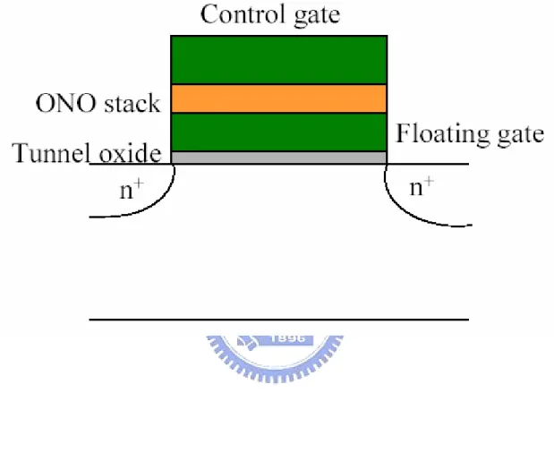
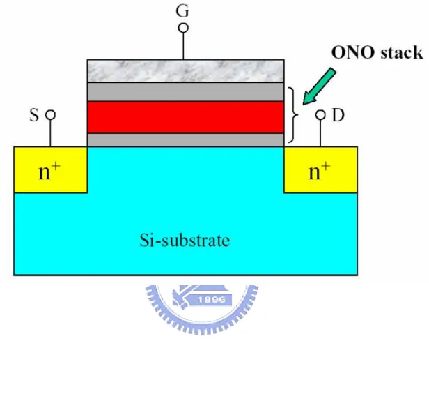
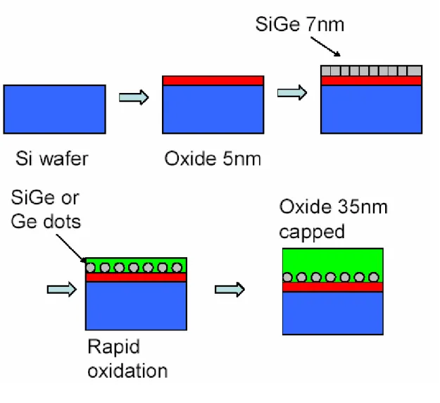
(11) Figure Captions Chapter 1 Fig. 1-1. The structure of the conventional floating gate nonvolatile memory device. Continuous poly-Si floating gate is used as the charge storage element and ONO sandwiched structure is used as the control oxide.. Fig. 1-2. The structure of the SONOS nonvolatile memory device. The nitride layer is used as the charge-trapping element.. Fig. 1-3. The structure of the nanocrystal nonvolatile memory device.. Chapter 2 Fig. 2-1. The process flow of fabricating Ge nanocrystals by rapid oxidation.. Fig. 2-2. Ge nanocrystals formed after high temperature rapid thermal annealing in N2 gas. The insert shows the gate stack in this study.. Fig. 2-3. The hysteresis of capacitance-voltage (C-V) measurements after 5V and –5V sweeping.. Fig. 2-4. (a) The leakage current of the gate dielectric with and without Ge nanocrystals. Fig. 2-4. (b) The relation of ln(J/E2) versus (1/E) shows the conduction mechanism is F-N tunneling and the insert shows the band diagrams of writing and erasing operation.. Fig. 2-5. The threshold-voltage shift is measured with different periods of time when the sample is heated at 150 ℃.. Fig. 2-6. Output characteristics of Ge Nanocrystal nonvolatile memory devices.. viii.
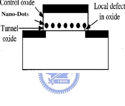
(12) Fig. 2-7. Transfer characteristics of Ge Nanocrystal nonvolatile memory devices.. Fig. 2-8. The Raman spectrum of the gate stack after the capping of control oxide. It is clearly observed that germanium precipitation is formed after the oxidation process of SiGe layer.. Fig. 2-9. The C-V hysteresis of the gate stack after the densification of the control oxide. The pronounced memory effects of the Ge nanocrystals embedded in silicon dioxide are shown with different programming voltages.. Chapter 3 Fig. 3-1. The cross-sectional TEM micrograph of an oxide/GeO2 nano-dots/oxide stacked structure.. Fig. 3-2. The XANES spectra of the investigated sample and standard samples.. Fig. 3-3. The capacitance-voltage hysteresis after the bidirectional bias sweeps between 5 V and (-5) V.. Fig. 3-4. The band diagrams of the operation of the novel distributed charge storage with GeO2 nano-dots.. Chapter 4 Fig. 4-1. The structure of the nanocrystal nonvolatile memory device. The semiconductor or metal nano-dots are used as the charge storage element instead of the continuous poly-Si floating gate.. Fig. 4-2. The process flow of fabricating Pt nanocrystals by e-beam evaporation. Fig. 4-3. The capacitance-voltage hysteresis after the bidirectional bias sweeps between 3 V and (-7) V.. Fig. 4-4. The capacitance-voltage hysteresis after the bidirectional bias sweeps between 3 V and (-7) V and between 5 V and (-7) V.. ix.
(13) Chapter 1. Introduction. 1.1 General Background. Since the demonstration of the MOSFET in 1960, one of the most revolutionary technology driver to decide the direction of semiconductor industries development is semiconductor memory. In 1967, D. Kahng and S. M. Sze invented the first floating-gate (FG) nonvolatile semiconductor memory at Bell Labs [1.1]. To date, the stacked-gate FG device structure, as shown in Fig. 1-1, continues to be the most prevailing nonvolatile-memory implementation, and is widely used in both standalone and embedded memories. The invention of FG memory impacts more than the replacement of magnetic-core memory, and creates a moment of portable electronic systems. The most widespread memory array organization is the so-called Flash memory, which has a byte-selectable write operation combined with a sector “flash” erase. Compared with DRAM, flash memory with floating gate structure ensures low power and long retention time and has much high array density. Although a huge commercial success, conventional FG devices have their limitations. The most prominent one is the limited potential for continued scaling of the device structure. This scaling limitation stems from the extreme requirements put on the tunnel oxide layer. In general, the tunnel oxide has to enable quick and efficient charge transfer to and from the FG. Moreover, the tunnel oxide needs to provide superior isolation under retention, endurance, and disturbed conditions in order to maintain information 1.
(14) integrity over periods of up to a decade. Once the deterioration of the tunnel oxide has been created because of the high electric fields across isolator, all the stored charge in the floating gate will be lost. However, when the tunnel oxide is thin enough to achieve the speed consideration, the retention characteristics may be degraded. Even though the tunnel oxide is made thicker to provide superior isolation for retention, the speed of the operation will be slower. As a result, there is a tradeoff between speed and reliability and the thickness of the tunnel oxide is compromised to about 8-11 nm, which is barely reduced over more than five successive generations of the industry [1.2]. Recently, two promising candidates are introduced, SONOS [1.3-1.5], as shown in Fig. 1-2, and nanocrystal nonvolatile memory devices [1.6-1.8], to overcome the scaling limits of the conventional FG structure. In both cases, retention time and endurance are superior to be expected from FG device observed for such thin oxides because of the intrinsic distributed charge storage [1.5]. Tiwari et al. [1.6] for the first time demonstrated the Si nanocrystal floating gate memory device in the early nineties. As shown in Fig. 1-3, the local leaky path will not cause the fatal loss of information for the nanocrystal nonvolatile memory device. Also, the nanocrystal memory device permits operation at low power with logic-compatible voltage while using CMOS-compatible processing [1.6-1.8].. 1.2 Nanocrystal Nonvolatile Memory Devices. Due to the drawbacks of the conventional FG device prone to failure of the FG isolation, nanocrystal nonvolatile memory with the FG of the distributed charge storage structure and long-term nonvolatility was introduced. The term “nanocrystal” refers to a crystalline structure whose dimensions are small enough to the nanometer 2.
(15) scale that its electronic properties begin to resemble those of an atom or molecule rather than those of the bulk crystal. At this scale, the size of a crystal can be used to directly manipulate its electronic and optical properties. Alivisatos gave a brief review of the electrical and optical properties of semiconductor clusters, nanocrystals, and quantum dots [1-9]. Currently, nanocrystal layers are being investigated for use in storage device, and semiconductor lasers. Nanocrystal nonvolatile memories, first introduced in the early 1990s, are one particular implementation of that concept. In a nanocrystal nonvolatile semiconductor memory (NVSM) device, charge is stored on a layer of discrete, mutually isolated, crystalline nanocrystals or dots. Each dot will typically store only a handful of electrons; collectively the charges stored in these dots control the channel conductivity of the memory transistor. As compared with conventional floating gate NVSM devices, nanocrystal charge storage permits using thinner tunnel oxide without sacrificing nonvolatility. This advantage results in lowering operating voltages and/or increasing operating speeds. The claim of improved scalability results not only from the distributed nature of the charge storage, which makes the storage more robust and fault-tolerant, but also from the beneficial effects of Coulomb blockade [1.7]. Quantum confinement effects (bandgap widening; energy quantization) can be exploited in sufficiently small nanocrystal geometries (sub-3 nm dot diameter) to further enhance the memory’s performance. There are other important advantages though. First, nanocrystal memories use a more simplified fabrication process and avoid the fabrication complications and costs of a dual-poly process. Further, because of the absence of drain to FG coupling, nanocrystal memories suffer less from drain induced barrier lowering (DIBL) and therefore have intrinsically better punchthrough characteristics. One way to exploit this advantage is to use a higher drain bias during the read operation, thus improving 3.
(16) memory access time. Alternatively, it allows the use of shorter channel lengths and therefore smaller cell area (i.e., lower cost). Finally, nanocrystal memories are characterized by excellent immunity to stress induced leakage current (SILC) and oxide defects for the distributed nature of the charge storage in the nanocrystal layer. Therefore, the performance and the success of the nanocrystal memory structure strongly depend on (a) the process ability for making uniform and reproducible thin tunnel oxides and (b) the characteristics of the islands (such as crystallinity, size, spatial distribution) that influence both the potential energy of trapped electrons and the Coulomb blockade energy, which prevent the injection and storage of more electron. However, there are some intrinsic weaknesses as well. Of particular importance is the low capacitive coupling between the external control gate and the nanocrystal charge storage layer. This does not only results in higher operating voltages, thus offsetting the benefits of the thinner tunnel oxide, it also removes an important design parameter (the coupling ratio) typically used to optimize the performance and reliability tradeoff. For the fabrication processes, a first requirement is the aerial density of the nanocrystal dots. A typical target is a density of at least 1012 cm-2. This is equivalent to approximately 100 particles controlling the channel of a memory FET with 100×100 nm2 active area, and requires particle size of 5-6 nm and below. Second, the fabrication process should result in a planar nanocrystal layer, i.e., the thickness of the dielectric layer separating the nanocrystal and the substrate should be well controlled. Moreover, good process control is needed with regards to such nanocrystal features as: size and size distribution, inter-crystal interaction (lateral isolation), uniformity of aerial crystal density, and crystal doping (type and level). Besides, the fabrication process is simple and be CMOS compatible with standard semiconductor equipments. Several nanocrystal fabrication processes have been demonstrated. Kim et al. [1.10] 4.
(17) fabricated high density Si nanocrystals of about 5×10¹¹/cm2 on nitride surface by conventional LPCVD [1.11-1.12]. Kanjilal et al. demonstrated Ge nanodots embedded in SiO2 by molecular beam epitaxy (MBE) [1.13]. The fabrication of Ge nanocrystals by the oxidation of SiGe contained films has been utilized [1.14]. As the SiGe layer is oxidized, the Ge element will be downward segregated and Si will be oxidized into SiO2 [1.15-1.27]. Ostraat et al. proposed an aerosol silicon nanocrystal nonvolatile memory device with large threshold voltage shift ( >. 3V),. sub-microsecond program times, millisecond erase times, excellent endurance (>105 program/erase cycles), and long term nonvolatility (>106 sec) [1.28]. Differing from the required single planar nanocrystal layer, Ohba et al. proposed a novel Si dot memory whose floating gate consists of self-aligned doubly stacked Si dots. Experiment shows that charge retention is improved compared to the usual single layer Si dot memory and be consistent with theoretical model [1.29]. Qu et al. presented an approach for synthesizing Ge nanocrystals embedded in amorphous silicon nitride films by plasma enhanced chemical vapor deposition (PECVD) [1.30]. As the size and size distribution of the nanocrystals have been considered, She et al. [1.31] made a conclusion on Ge nanocrystal memory device that nanocrystal size around 5 nm is preferred to achieve fast programming speed and longer retention time, and the size should not be scaled below that. The quantum confinement effect for Ge nanocrystals smaller than 5 nm is very significant so that the retention time is shorter and the programming time is longer. Park et al. [1.32] also utilized PECVD to form Si nanocrystals embedded in silicon nitride film. Capacitance-voltage hysteresis is used to inspect the memory effects of the nanocrystal memory devices [1.33]. In addition to semiconductor nanocrystals, Liu et al. described the design principles and fabrication processes of metal nanocrystals [1.34-1.35]. The advantages of metal nanocrystals over their semiconductor counterparts include higher density of states, 5.
(18) stronger coupling with the channel, better size scalability, and the design freedom of engineering the work functions to optimize the device characteristics. Due to the minimization of the surface energy of the metal film under rapid thermal annealing, the driving force results in a discrete layer of metal nanocrystals reside on tunnel oxide. Baik et al., proposed a tunnel barrier structure that is composed of silicon dioxide and amorphous carbon (a-C) to attain enhanced charge retention without degradation in the injection efficiency [1.36]. Additionally, high-k tunnel dielectrics were investigated for Si nanocrystal memory devices [1.37-1.39]. Results show that the use of high-k dielectric on Si channel results in faster programming and longer retention because of its asymmetry band structure in programming and retention mode. Besides, the programming and erasing mechanisms of p-channel nanocrystal memory devices were also investigated by Han et al. [1.40]. The comparison of retention between programmed holes and electrons shows that holes have longer retention time. Over the past decade, the benefits of a charge-storage memory device which exceeds the performance limits of conventional floating gate device has attracted a great deal of interests and spurring rapid progress in this area. By using isolated charge storage in tunneling oxide, charge leakage through localized defeats is greatly reduced; consequently, thinner tunneling oxide for the fast write/erase speed, low power can be employed. Research in this area has been focused on the development of nanocrystal materials and fabrication processes, and on the integration of nanocrystal-based storage layers in actual memory devices. In spite of these promising results, it is unclear whether nanocrystal memories will ever see commercialization. In order for that to happen, the uniformity of the nanocrystals needs to be improved, and the claimed benefits need to be more unambiguously substantiated.. 6.
(19) 1.3 Organization of the Thesis. This thesis is divided into three chapters. The contents in each chapter are described as follows. In chapter 2, a novel approach of fabricating germanium nanocrystals for nonvolatile memory applications is presented. In chapter 3, the nonvolatile semiconductor memory with the distributed charge storage GeO2 nanodots is demonstrated in this chapter. In chapter 4, the electron charging and discharging effects of metal nanocrystals embedded in silicon dioxide for low-power nonvolatile memory technology are demonstrated. Finally, the summarization of all experimental results in this dissertation and the suggestions for the future work are presented in chapter 5.. 7.
(20) Figure 1-1 The structure of the conventional floating gate nonvolatile memory device. Continuous poly-Si floating gate is used as the charge storage element and ONO sandwiched structure is used as the control oxide.. 8.
(21) Figure 1-2 The structure of the SONOS nonvolatile memory device. The nitride layer is used as the charge-trapping element.. 9.
(22) Nano-Dots. Figure 1-3 The structure of the nanocrystal nonvolatile memory device. The semiconductor or metal nano-dots are used as the charge storage element instead of the continuous poly-Si floating gate.. 10.
(23) Chapter 2. Nonvolatile Memory with Distributed Germanium Nanocrystal Storage. 2.1 Introduction. Since the demonstration of the MOSFET in 1960, one of the most revolutionary technology driver to decide the direction of semiconductor industries development is semiconductor memory. In 1967, D. Kahng and S. M. Sze invented the first floating-gate (FG) nonvolatile semiconductor memory at Bell Labs [2.1]. Although there is a huge commercial success, conventional FG devices have their limitations. The most prominent one is the limited potential for continued scaling of the device structure. Conventional floating gate non-volatile memory (FG-NVM) present critical issues for scaling the device structure at sub-90nm node, due to severe internal burdens, like gate length and tunneling oxide thickness [2.2]. The tunnel oxide has to allow quick and efficient charge transfer to and from the FG. However, the tunnel oxide needs to provide superior isolation under retention and disturbed conditions in order to maintain information integrity over periods of up to a decade. Once the deterioration of the tunnel oxide has been created because of the high electric fields across isolator, all the stored charge in the floating gate will be lost. However, when the tunnel oxide is thin enough to achieve the speed consideration, the retention characteristics may be degraded. Even though the tunnel oxide is made thicker to provide superior isolation for retention, the speed of the operation will be slower. As a result, there is a tradeoff between speed and reliability and the thickness of the tunnel. 11.
(24) oxide is compromised to about 8-11 nm, which is barely reduced over more than five successive generations of the industry [2.3]. Nanocrystal dots within semiconductor materials have attracted particular attention because of the possibility of integrating dots with novel or superior properties into existing micro- and opto-electronic technologies. Nanocrystal memory, the size of a crystal on the order of 1-100nm, can be used to directly manipulate its electronic and optical propertyies and the nanocrystal memory can maintain good retention characteristics when tunnel oxide is thinner and lower the power consumption [2.4-2.6]. In principle, nanocrystal dots with specific properties can be precisely tailored for specific applications, making them enormously useful in wide variety of technologies. Silicon (Si) and germanium (Ge) nanocrystal memories has serious potential for pushing further the scaling limits of conventional NVMS with fully CMOS compatible technology based on discrete storage nodes [2.7]. In this chapter, we proposed a Ge nanocrystal memory device with 4.5nm-thick tunnel oxide and a low operating voltage of 5V, and a significant threshold-voltage shift due to the charge trapping in the Ge dots is observed.. 2.2 Experimental procedures. 2.2.1 Germanium Nanocrystals Formation. This charge-trap based nonvolatile memory structure can be fabricated using conventional wafer-processing techniques. Prior to SiGe deposition, the 6-in Si wafer was cleaned with standard RCA clean, followed by thermal oxidation process to form 4.5nm-thik dry SiO2 layer as tunneling oxide in an atmospheric pressure chemical vapor deposition (APCVD) furnace. Right after the growth of tunnel oxide, 12.
(25) poly-Si0.8Ge0.2 was formed on the oxide immediately by low pressure chemical vapor deposition (LPCVD). The deposition of Si0.8Ge0.2 was kept at 550℃ and the pressure was controlled to be 460 mTorr. The flow rate of the reaction gas of SiH4 and GeH4 was 60 and 8 sccm, respectively, and the Ge fraction was analyzed to be around 0.2 by Auger electron spectroscopy (AES). Subsequently, the Si0.8Ge0.2 layer was wet oxidized in an APCVD reactor and the Ge atoms would be segregated downward until they reach the tunnel oxide surface [2.8-2.10]. Then, a rapid thermal annealing (RTA) at 950℃ in N2 ambient was performed to form the Ge nanocrystals. The melting point of Ge was ~938℃. Therefore, the N2 RTA at 950℃ transformed the Ge layer to liquid phase and the Ge nanocrystals formed after cooling down. In addition, it was well known that during the oxidation of SiGe, GeO2, a weakly bonded molecule, was created. The 950℃ N2 RTA would reduce the Ge atoms and the nanocrystals grew based on the Ostwald ripening mechanism [2.11], in which the larger dots grew at the expense of the smaller dots. From the analysis of transmission electron microscopy (TEM), the control oxide capped on the Ge nanocrystals was estimated to be about 40nm. Also, the sample without Ge nanocrystals was fabricated as a control sample. It is fabricated by depositing a poly-Si layer on the tunnel oxide, followed by the wet oxidation of poly-Si layer, the same process done as the silicon germanium layer. The thickness of the oxide fabricated by oxidizing the poly-Si is measured by n&k analyzer, and fine-tuned to be 40 nm. Finally, the Al electrode was patterned and sintered. The metal-insulator-semiconductor (MIS) structure with Ge nanocrystals embedded between tunnel and control oxide was fabricated. In this work, the formation of Ge nanocrystals is only by one step of oxidation of the silicon-germanium layer, which is simpler than the previous research [2.6] and high-throughput and low cost potentially for industrial consideration. Moreover, the above method was utilized to fabricate the MOSFET nanocrystal 13.
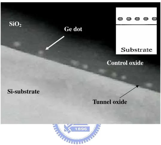
(26) nonvolatile memory device.. 2.2.2 The Novel Concept of Nonvolatile Memory with Thin Silicon Germanium Oxidation along Grain Boundary. In addition to the fabrication method of forming Ge nanocrystals demonstrated in this chapter, a more flexible and direct approach is proposed in the supplement. Figure 2-1 illustrates the process flow of fabricating Ge nanocrystals by rapid thermal oxidation. After the p-type Si wafer was RCA cleaned, a 5nm-thick dry oxide was thermally grown as the tunnel oxide at 925 ℃ in an atmospheric pressure chemical vapor deposition furnace. Subsequently, a 7nm-thick SiGe layer was deposited at 450 ℃ by low pressure chemical vapor deposition, followed by a rapid thermal oxidation at 925 ℃. During the oxidation process, the oxidation of SiGe will be conducted faster along the grain boundary than that of the grain of the SiGe layer and the oxidation mechanism of SiGe is as described as the beginning of this chapter. After the oxidation of SiGe was performed, a 35nm-thick TEOS oxide is capped as the control oxide, followed by the process of steam densification to densify the control oxide.. 2.3 Results and discussions. 2.3.1. The Memory Effect of Germanium Nanocrystal Nonvolatile Memory. A cross-sectional TEM of an oxide/Ge dots/oxide stacked structure is shown in Fig. 2-2. It is clearly shown the Ge nanocrystals are embedded between tunnel oxide and 14.
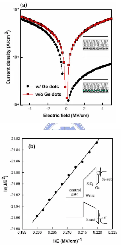
(27) control oxide, which are oxidized from the Si0.8Ge0.2, and are separated from each other. The insert schematically shows the gate stack arrangement in this study. The size of the dots is estimated to be about 5.5nm by TEM. She et al. [2.12] made a conclusion on Ge nanocrystal memory device that nanocrystal size around 5nm is preferred to achieve fast programming speed and longer retention time, and the size should not be scaled below that. The quantum confinement effect for Ge nanocrystals smaller than 5nm is very significant so that the retention time is shorter and the programming time is longer. In this work, the fabricated Ge dots satisfy the demand. Figure 2-3 shows the hysteresis curves of capacitance-voltage (C-V) measurements after a bias sweeping from –5V to 5V. It is found that a low operating voltage, 5V, causes a significant threshold-voltage shift up to ~0.42V, which is enough to be defined as 1 or 0 for the circuit design. Due to the discrete distribution of the Ge dots and Coulomb blockade effect, the capacitance coupling of the nanocrystal memory device is lower than that of the conventional floating gate memory device. If the capacitive coupling is low to the Ge nanocrystals, the threshold-voltage shift may come from the oxide traps. To distinguish the blur, C-V measurement of sample without Ge dots was preformed (not shown therein). It is found after 5-V write operation that there is almost no Vt shift (lower than 0.01V) for the sample without Ge dots. The threshold-voltage shift resulted from oxide traps is thereby negligible. The density of Ge dots can be electrically calculated through the threshold-voltage shift, ∆Vt, by the following expression: ∆Vt =. t control. ε ox. ⋅Q t. where εox is the permittivity of SiO2, tcontrol the thickness of the control oxide, and Qt is the density of the trapped charge (C/cm2 in unit) in Ge nanocrystals. Setting tcontrol = 40nm, ∆Vt = 0.42V, and εox = 3.9×8.85×10-14 F/cm, the number of electrons trapped in 15.
(28) the Ge nanocrystals was calculated to be 2.3×1011 cm-2. Due to Coulomb Blockade effect, presumably only one electron was trapped in each Ge nanocrystal [2.4, 2.13]; hence, the aerial density of the Ge dots is about 2.3×1011 cm-2. Figure 2-4 (a) shows the leakage current of the gate dielectric with and without Ge nanocrystals under substrate and gate injection bias. It is clearly shown that under substrate injection bias the leakage of the gate oxide stack with Ge nanocrystals is lower than that without Ge dots. It can be deduced that when the first electron enters into the nanocrystal, the effect of Coulomb blockade [2.13] prevents further injection and storage of more electrons and decreases the leakage current. The reduction in leakage current makes the storage of charges more robust and fault-tolerant. That is, therefore, one of the reasons that nanocrystal memory devices exhibit more rugged retention characteristics than conventional FG ones [2.5]. As considering the leakage current under gate injection bias, there is only little difference between the samples with and without Ge dots due to the lack of Coulomb blockade effect. The conduction mechanism among the gate-dielectric stack with Ge dots is inferred from Fowler-Nordheim (F-N) tunneling [2.14] which can be expressed as follows: ⎡ 8π 2m * (qφ ) 3 / 2 ⎤ B J = E exp ⎢− ⎥ 3 qhE ⎢⎣ ⎥⎦ 2. where E is the electric field which is defined as the applied voltage divided by total thickness of the tunnel and control oxide, m* the electron effective mass, h the Planck’s constant, φB the energy barrier at the injecting interface (3.1eV for Si-SiO2), and ln(J/E2) is proportional to (1/E). In Fig. 2-4 (b), after the transformation of Fig. 4-3 (a), it is clearly found there is a linear region in high field, which proves the conducting mechanism with Ge dots embedded in the oxide stack is F-N tunneling. The layer without Ge dots embedded also creates a well-fitted F-N plot at high field, which is not shown therein. Also, the insert exhibits the band diagrams of F-N 16.
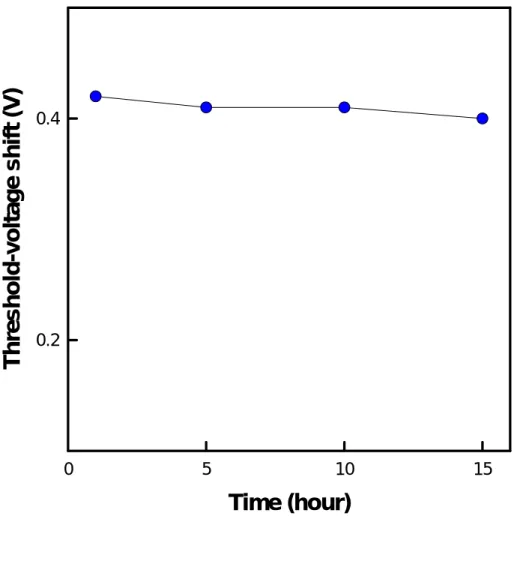
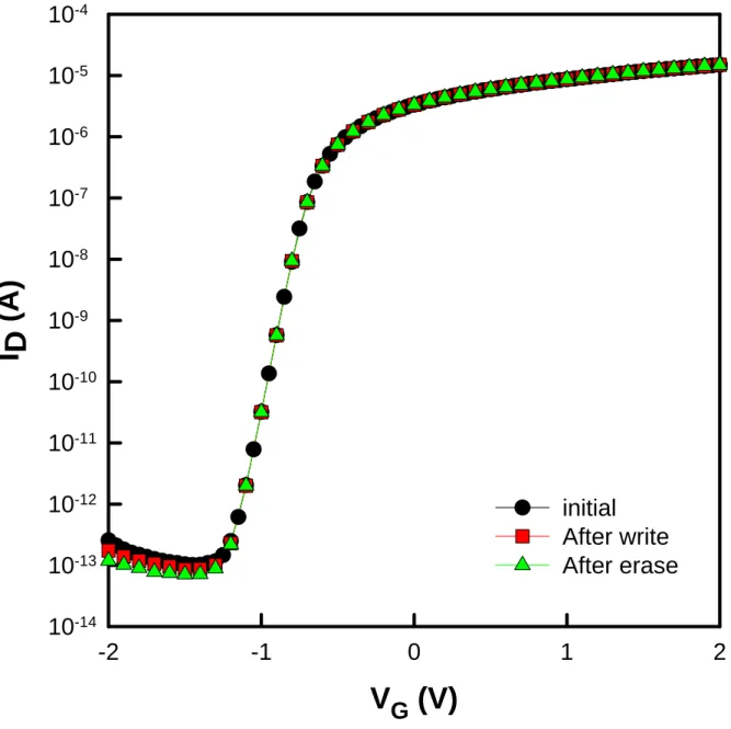
(29) tunneling for writing and erasing operation in this study. In addition, to realize the retention characteristics of the structure, a stricter test environment of 150 ℃ is conducted [2.15, 2.16]. In Fig. 2-5, the threshold-voltage shift is measured with different periods of time when the sample is heated at 150 ℃. It is found that the oxide stack with Ge dots embedded retains a good retention property without a significant decline of the memory window, ∆Vt, up to 15 hours, which is robust in the Flash nonvolatile memory technology. As shown in Fig. 2-6 , the output characteristics of Ge nanocrystal nonvolatile memory device are with the gate voltage 0V, 4V, 8V, 12V, 16V, and 20V respectively. Figure 2-7 shows the transfer characteristics of Ge nanocrystal nonvolatile memory device with initial state (without write and erase), after write, and after erase. Obviously, although we have succeeded in the manufacturing of the MOSFET device, from the transfer characteristics of Ge nanocrystal nonvolatile memory device it is clearly observed that there is almost no difference between the threshold voltage of the device after write and erase. This electrical performance results from that the germanium is not bonding with silicon when we deposited silicon germanium by low pressure furnace, and after the oxidation of silicongermanium there are no germanium nanocrystals precipitated between control oxide and tunneling.. 2.3.2 The Observation of Germanium Precipitation of the Rapid Oxidation of Silicon Germanium in Raman Spectroscopy. In this approach, the rapid oxidation of SiGe was intended to fabricate SiGe nanodots embedded in silicon dioxide after the oxidation along the grain boundary of the SiGe layer. Until the silicon element was completely consumed to SiO2 during the oxidation process, the Ge nanodots were precipitated and reside on the tunnel oxide 17.
(30) layer. It is deduced that under an appropriate control of the rapid oxidation of the SiGe layer, SiGe or Ge nanodots can be fabricated as expectation. As shown in Fig. 2-8, the Raman spectrum of the gate stack after the capping of control oxide exhibits that the germanium precipitation is formed at wave number of ~ 300 cm-1 and there is no absorption of SiGe precipitation at ~ 400 cm-1 after the oxidation process of SiGe layer. It is deduced that the oxidation time is long enough to fully oxidize the Si element of the SiGe layer and the Ge nanodots are segregated. Figure 2-9 shows the C-V hysteresis of the gate stack after the densification of the control oxide. The pronounced memory effects of the Ge nanocrystals embedded in silicon dioxide are shown with different programming voltages. The memory window of the memory device is increased with the programming voltage. To ensure the realization of the memory device, further investigation of the memory device needs to be taken into account.. 2.4 Conclusion. A nonvolatile memory device embedded with Ge nanocrystal dots is fabricated by the thermal oxidation of Si0.8Ge0.2 combined with a rapid thermal annealing at 950℃ in N2 gas. The tunnel oxide in the nonvolatile memory is controlled to be 4.5 nm-thick and embedded with 5.5-nm Ge nanocrystals. A low operating voltage, 5V, is implemented and a significant threshold-voltage shift, 0.42V, is observed. When the electrons are trapped in the Ge nanocrystals, the effect of Coulomb blockade prevents the injection and storage of more electrons and decreases the leakage current. Also, the retention characteristics are tested to be robust.. 18.
(31) Figure 2-1 The process flow of fabricating Ge nanocrystals by rapid oxidation.. 19.
(32) SiO2. Ge dot. Control oxide. Si-substrate Tunnel oxide. Figure 2-2 Ge nanocrystals formed after high temperature rapid thermal annealing in N2 gas. The insert shows the gate stack in this study.. 20.
(33) 1.2. 1.0. C/Cox. 0.8. 5V~(-5)V -5V~5V 0.6. 0.4. 0.2. 0.0 -4. -2. 0. 2. 4. Voltage (V). Figure 2-3 The hysteresis of capacitance-voltage (C-V) measurements after 5V and –5V sweeping.. 21.
(34) (a). Figure 2-4 (a) The leakage current of the gate dielectric with and without Ge nanocrystals (b) The relation of ln(J/E2) versus (1/E) shows the conduction mechanism is F-N tunneling and the insert shows the band diagrams of writing and erasing operation. 22.
(35) Threshold-voltage shift (V). 0.4. 0.2. 0. 5. 10. 15. Time (hour). Figure 2-5 The threshold-voltage shift is measured with different periods of time when the sample is heated at 150 ℃.. 23.
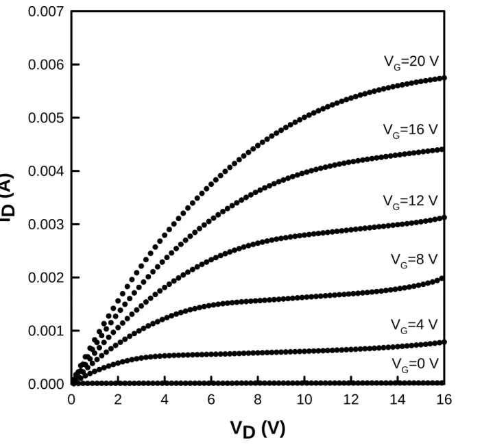
(36) 0.007. VG=20 V. 0.006. ID (A). 0.005. VG=16 V. 0.004 VG=12 V 0.003 VG=8 V 0.002 VG=4 V. 0.001. VG=0 V 0.000 0. 2. 4. 6. 8. 10. 12. 14. 16. VD (V). Figure 2-6 Output characteristics of Ge Nanocrystal nonvolatile memory devices.. 24.
(37) 10-4 10-5 10-6 10-7. ID (A). 10-8 10-9 10-10 10-11 10-12. initial After write After erase. 10-13 10-14 -2. -1. 0. 1. 2. VG (V). Figure 2-7 Transfer characteristics of Ge Nanocrystal nonvolatile memory devices.. 25.
(38) Intensity (A. U.). Intensity (A. U.). Si-Ge. Ge-Ge. as-deposited Ge-Ge. 200. 300. 400. 500. 600. after oxidation. Raman shift (cm-1) 200. 300. 400. 500. 600. Raman shift (cm-1). Figure 2-8 The Raman spectrum of the gate stack after the capping of control oxide. It is clearly observed that germanium precipitation is formed after the oxidation process of SiGe layer.. 26.
(39) 280 260. Capacitance (pF). 240 220 200 180 160 140 120 100 80 -10. 5V ~ (-7)V -7V ~ 5V 10V ~ (-10)V -10V ~ 10V -8. -6. -4. -2. 0. 2. Voltage (V). Figure 2-9 The C-V hysteresis of the gate stack after the densification of the control oxide. The pronounced memory effects of the Ge nanocrystals embedded in silicon dioxide are shown with different programming voltages.. 27.
(40) Chapter 3. Nanocrystal Nonvolatile Memory with Distributed GeO2 Nanodots. 3.1 Introduction. In the age of 1960’s, MOSFET was demonstrated. One of the most revolutionary technology driver to decide the direction of semiconductor industries development is semiconductor memory. In 1967, D. Kahng and S. M. Sze invented the first floating-gate (FG) nonvolatile semiconductor memory at Bell Labs [3.1]. Conventional floating –gate non-volatile memory (FG-NVM) present critical issues for scaling the device structure at sub-90nm node, due to severe internal burdens, like gate length and tunneling oxide thickness [3.2]. Silicon (Si) and germanium (Ge) nanocrystal memories has serious potential for pushing further the scaling limits of conventional NVMS with fully CMOS compatible technology based on discrete storage nodes [3.3]. Silicon (Si) and germanium (Ge) of the discrete nanocrystals in SiO2 layers has been studied by a large number of groups and strong memory effects in MOS devices were reported. Nonvolatile MOS memory devices employing silicon, germanium nanocrystal charge-storage sites produced by ion implantation into the gate oxide have been demonstrated in recent studies. However, limitations of the ion implantation technique place a lower limit on the gate oxide thickness. In addition, ion implantation may compromise the integrity of oxides. In this study, we proposed a concept for creating GeO2 charge-trap sites within the gate dielectric of a MOS structure.. 28.
(41) 3.2 Experimental procedures. This charge-trap based nonvolatile memory structure can be fabricated using conventional wafer-processing techniques. Prior to SiGe deposition, the 6-in Si wafer was cleaned with standard RCA clean, followed by thermal oxidation process to form 4.5nm-thik dry SiO2 layer as tunneling oxide in an atmospheric pressure chemical vapor deposition (APCVD) furnace. Right after the growth of tunnel oxide, poly-Si0.8Ge0.2 was formed on the oxide immediately by low pressure chemical vapor deposition (LPCVD). The deposition of Si0.8Ge0.2 was kept at 550℃ and the pressure was controlled to be 460 mTorr. The flow rate of the reaction gas of SiH4 and GeH4 was 60 and 8 sccm, respectively, and the Ge fraction was analyzed to be around 0.2 by Auger electron spectroscopy (AES). Subsequently, the Si0.8Ge0.2 layer was oxidized in an APCVD reactor and the Ge atoms would be segregated downward until they reach the tunnel oxide surface [3.4-3.6]. The Ge dots grew based on the Ostwald ripening mechanism [3.7], in which the larger dots grew at the expense of the smaller dots. After the Si elements of the Si1-xGex layer are completely oxidized, the Ge nanocrystals tend to be oxidized into GeO2 nano-dots as the oxidation process is not ceased. From the analysis of transmission electron microscopy (TEM), the control oxide capped on the GeO2 nano-dots was estimated to be about 40 nm and the GeO2 nano-dots were confirmed via x-ray absorption near-edge structure (XANES). Finally, the Al electrode was patterned and sintered. Electrical measurements were performed on the metal-insulator-semiconductor (MIS) structures with GeO2 nano-dots embedded between tunnel and control oxide.. 3.3 Results and discussions 29.
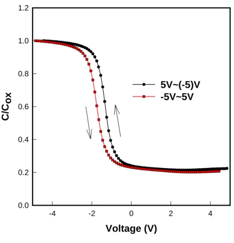
(42) A cross-sectional TEM micrograph of an oxide/GeO2 nano-dots/oxide stacked structure is shown in Figure 3-1. It is clearly observed the GeO2 nano-dots are embedded between the tunnel oxide and control oxide, oxidized from the Si1-xGex layer, and are separated from each other. The insert schematically shows the gate stack arrangement in this study. The mean size and aerial density of the dots are estimated to be about 5.5 nm and 4.3×1011 cm-2, respectively, by TEM. To confirm the existence of the composition of the GeO2 nano-dots, x-ray absorption near-edge structure (XANES) is performed [3.8-3.10]. In XANES, a core electron is excited to higher bound or quasi-bound states, which contain information about coordination geometry and electronic aspects of the absorbing atom. Among most of the XANES studies, the standard materials with known valence is utilized as references, and compared with the unknown samples. Therefore, the measurements are frequently qualitatively-analyzed, not quantitatively. In this work, we used Ge powder, GeO2 powder, and Si0.8Ge0.2 epitaxial layer on Si as the standard materials and our investigated sample with nano-dots observed as the unknown sample. The x-ray source is extracted from the National Synchrotron Radiation Research Center. As shown in Figure 3-2, the shift of absorption edge (roughly the center of the intensity jump) is an index of the Ge oxidation state. The obvious edge shift from the Ge edge and the high degree of similarity between the XANES results of the sample with nano-dots and GeO2 standard reveal that Ge is oxidized. Its oxidation state is very close to GeO2. Figure 3-3 shows the capacitance-voltage (C-V) hysteresis after the bidirectional bias sweeps between 5 V and (-5) V. It is found that a low operating voltage, 5 V, causes a significant threshold-voltage shift up to ~0.45 V, which is sufficient to be defined as “1” or “0” for the logic-circuit design. It is worth noting that the hysteresis 30.
(43) is counterclockwise which is due to substrate injection from the electrons of the deep inversion layer and holes of the deep accumulation layer of the Si substrate [3.11]. Figure 3-4 demonstrates the band diagrams of the operation of the novel distributed charge storage with GeO2 nano-dots. The “write” and “erase” operation with different gate polarities of the memory device are exhibited. When the device is written or programmed, the electrons directly tunnel from the Si substrate through the tunnel oxide, and are trapped in the GeO2 nano-dots. When the device is erased, the electrons may tunnel back to the deep accumulation layer of Si substrate. The control oxide is utilized to prevent the carriers of gate electrode from injecting into the GeO2 nano-dots by Fowler-Nordheim (F-N) tunneling. It is believed that during the oxidation process of the Ge nanocrystals into GeO2 nano-dots, there are defects or traps created in the interfaces between GeO2 dots and tunnel and control oxide. When the device is under programming, the injected electrons will be captured in the interfacial traps of the GeO2 dots and contribute to a threshold voltage shift (memory window). It is concerned about that if the storage of GeO2 nano-dots is as reliable as other insulating thin films. The reliability issues such as endurance and retention of the memory device should be taken into account and are currently under investigation.. 3.4 Conclusion. The novel distributed charge storage with GeO2 nano-dots is fabricated. The mean size and aerial density of the nano-dots embedded in SiO2 are estimated to be about 5.5 nm and 4.3×1011 cm-2, respectively. The composition of the dots is also confirmed to be GeO2 by x-ray absorption near-edge structure analyses. A significant memory effect is observed through the electrical measurements. Under the low voltage operation of 5 V, the memory window is estimated to ~0.45 V. Also, a physical model 31.
(44) is proposed to explain the charge storage effect through the interfacial traps of GeO2 nano-dots. Further works about the research on the reliability issues are currently under investigation.. 32.
(45) 20 nm. Figure 3-1 The cross-sectional TEM micrograph of an oxide/GeO2 nano-dots/oxide stacked structure.. 33.
(46) Figure 3-2 The XANES spectra of the investigated sample and standard samples.. 34.
(47) Figure 3-3 The capacitance-voltage hysteresis after the bidirectional bias sweeps between 5 V and (-5) V.. 35.
(48) charge trapping sites. e-. Ec Si-sub. SiO2 control gate. GeO2. Write. Erase. e-. Figure 3-4 The band diagrams of the operation of the novel distributed charge storage with GeO2 nano-dots.. 36.
(49) Chapter 4. Metal Nanocrystal Nonvolatile Memory device with Distributed Pt Nanodots. 4.1 Introduction. Memory with discrete charge elements allows more advanced scaling of tunneling oxide and exhibits superior characteristics compared to conventional floating gate memories in terms of operation voltage, write/erase speed, retention and endurance [4.1-4.5]. By fabricating the nonvolatile memory based on the charge-trap structure, the dynamic and physical operation can be expected to compete with DRAMs [4.6]. To achieve these purposes simultaneously, an asymmetry in charge transit through the gate oxide to optimize the IG, Write/Erase/IG, Retention ratio has been proposed. By replacing the charge storages of semiconductor nanocrystals with metal nanocrystals, we can engineer the depth of the potential well at the charge storage nodes, and an asymmetrical barrier between the substrate and the charge storage node could be created [4.7]. Because the work function of metal nanocrystals decides depth of the potential well at the charge storage nodes and the density of states available for tunneling in the substrate, by engineering the metal work function, the barrier height can be adjusted small for writing and large for retention due to its asymmetry band structure between the substrate and the charge storage nodes, that is, much freedom for devices and circuits design. Metal nanocrystal memory has attracted much attention recently for the advantages such as high density of states around the Fermi level, better coupling of the control 37.
(50) oxide and tunneling oxide, a wide range of available work functions, and smaller energy perturbation due to carrier confinement [4.8]. The high density of states makes metal nanocrystals more immune to Fermi-level fluctuation by contamination. Due to more uniform charging characteristics, the metal nanocrystal memory enables to have tighter threshold voltage control. For the wider range of the metal work function, we are promised to engineer the tradeoff between write/erase and charge retention. By aligning the nanocrystal Fermi level to be within the Si bandgap for retention and above the conduction band edge for erase, the better erase speed and long retention can be performed without leakage concern even for very thin tunneling oxide. Metal nanocrystal memory also provides more degree of design freedom and scalability for the nanocrystal size. Besides, for semiconductor nanocrystal memory, the band gap of nanocrystal is widened in comparison with that of the bulk materials due to the multidimensional carrier confinement, which reduces the effective depth of the potential well and compromises the retention time. This effect is much smaller in a metal nanocrystal because there are thousands of conduction band electrons in a nanocrystal even in charge neutral state. The device structure of metal nanocrystal memory is shown in Figure 4-1. The storage of electrons in individual nanocrystals of high density is separated from the channel by ultra thin oxide so that direct tunneling is the dominant mechanism for injection and extraction. Depending on the oxide thickness, the charge transport is dominated by either direct tunneling or F-N tunneling. As the result, with a repeatable process for metal nanocrystal memory of high density, metal nanocrystal can be incorporated into a standard MOSFET structure to fabricate nonvolatile memory devices, and metal nanocrystal memory is one of the candidates that have the potential to achieve fast write/erase and long retention time simultaneously.. 38.
(51) 4.2 Experimental procedures. This charge-trap based nonvolatile memory structure can be fabricated using current semiconductor equipment. Prior to Pt deposition, the 6-in Si wafer was cleaned with standard RCA clean, followed by thermal oxidation process to form 4.5nm-thik dry SiO2 layer as tunneling oxide in an atmospheric pressure chemical vapor deposition (APCVD) furnace. After the growth of tunnel oxide, a 2 nm distributed Pt layer is deposited onto the tunnel oxide by e-beam evaporation, followed by the capping of 15 nm amorphous Si layer by e-beam evaporation. Subsequently, the control oxide is fabricated by dry oxidation in an atmospheric pressure chemical vapor deposition (APCVD) furnace. Finally, Al gate electrode is patterned with thermal coater. Thus the MOS structure with distributed charge storage nodes is formed. All the basic procedure for Pt nanocrystal formation is shown in Fig 4-2. This structure is analyzed by transmission electron microscopy (TEM). The memory effect of the electron charging and discharging effects of the Pt nanocrystals is investigated in significant hysteresis phenomenon in capacitance-voltage (C-V) measurements by a precision LCR meter HP 4284A.. 4.3 Results and discussions. The work function of Pt is about 5.7 eV. By using Pt nanocrystals with larger work function, we can increase the barrier height seen by the electrons inside the nanocrystals. The increase of barrier height translates into reduced tunneling probabilities and enhanced charge retention. Therefore, the concept of work-function engineering can also be applied to conventional flash memory. However, the thermal 39.
(52) and mechanical incompatibility of metal film on top of ultra thin gate oxide makes the process difficult due to concerns of oxide integrity, interface states and channel carrier mobility. On the other hand, in nanocrystal memories those problems can be alleviated. through. self-assembled. nanocrystal. formation,. which. produces. thermodynamically stable structures and introduces minimal contaminations into the oxide and channel underneath [4.9-4.11]. The Pt nanodot is based on the self assembled nanocrystal formation with surface energy minimization. For thin film under 3 nm in thickness, nanocrystals can be seen even without annealing. After the oxidation of control oxide formation, well-defined nanocrystals with round shape and certain size distribution can be achieved. But, when the Pt film grows thicker, the deposited film shows more inter-links between nanocrystals and gradually transforms into irregular interlocked islands. After the oxidation of control oxide formation, the nanocrystals become bigger with wider and more irregular size distribution. When the film exceeds certain thickness threshold, islands remain after oxidation and no nanocrystals are formed. A significant memory effect is observed through the electrical measurements. Under the low voltage operation of 3 V for write and -7V for erase, the memory window is estimated to ~0.45 V as shown in Fig 4-3. The threshold voltage shifts are considered as the charge stored in the Pt nanocrystals. Due to the Coulomb blockade effect, the low power operation can be performed to enable single election or few electrons to be translated to Pt nanocrystals. However, under the same low voltage operation of 3 V for write and -7V for erase, the memory window is estimated to ~1.5 V and under the voltage operation of 5 V for write and -7V for erase, the memory window is estimated to ~2.2 V as shown in Fig 4-4. It is obviously found that the hysteresis is clockwise. In other words, after erase the threshold voltage is higher than that after write. This electrical performance results from two reasons. One reason is the quality of the control oxide. Because the control oxide is formed by the 40.
(53) oxidation of the electron sputtered silicon and the quality of electron beam sputtered silicon is not as perfect as that of silicon deposited by low pressure furnace. Thus after write, the hole inject from the metal gate across the control oxide to the Pt nanocrystal instead of the electron inject from the channel across the tunneling oxide to the Pt nanocrystals. The other reason is metal pollution during oxidation of the control oxide and it results in the mobile ions generated in control oxide. Further works about the research such as how to fabricate a well-performed control oxide and fabricate the uniformly distributed Pt dots are currently under investigation.. 4.3 Conclusion. We proposed a simple process to fabricate the metal nanocrystal nonvolatile memory which is one of the candidates that have potential of achieving fast write/erase and long retention time simultaneously. By engineering the work function, nonvolatile metal nanocrystal memory can be engineered to work either in direct tunneling mechanism or F-N tunneling mechanism. With a repeatable process for self assembled nanocrystal formation with controllable density and size distribution, we can incorporate metal nanocrystals into a standard MOSFET structure to fabricate nonvolatile memory devices.. 41.
(54) Nano-Dots. Figure 4-1 The structure of the nanocrystal nonvolatile memory device. The semiconductor or metal nano-dots are used as the charge storage element instead of the continuous poly-Si floating gate. 42.
(55) Si wafer. E-gun Pt 20A. Oxide 50A. Oxide 300A. and Si 150A. Figure 4-2 The process flow of fabricating Pt nanocrystals by e-beam evaporation. 43.
(56) 160 3V~-7V -7V~3V. 140. Capacitance (pF). 120. 100. 80. 60. 40. 20 -3. -2. -1. 0. 1. 2. 3. Voltage (V). Figure 4-3 The capacitance-voltage hysteresis after the bidirectional bias sweeps between 3 V and (-7) V. 44.
(57) 140 3V~-7V -7V~3V 5V~-7V -7V~5V. Capacitance (pF). 120. 100. 80. 60. 40. 20 -7. -6. -5. -4. -3. -2. -1. 0. 1. 2. 3. 4. 5. Voltage (V). Figure 4-4 The capacitance-voltage hysteresis after the bidirectional bias sweeps between 3 V and (-7) V and between 5 V and (-7)V. 45.
(58) Chapter 5. Conclusions and Suggestions for Future Work. 5.1 Conclusions. We have demonstrated the memory effect due to charge storage in nanodots of nanocrystal nonvolatile memory. Promising MOS related memory devices have been obtained that exhibit significant threshold voltage window at low bias voltage operations. The speed of the devices is dependent on the tunneling oxide thickness, and for thin tunneling oxide, the retention behavior can meet the long term nonvolatility requirement. Moreover, the experimental processes are under control with regard to such nanocrystal features as: size distribution, inter-crystal interaction (lateral isolation), and uniformity of aerial crystal density. Besides, all the fabrication procedures are simple and use CMOS compatible processing with standard semiconductor equipments.. 5.1.1 Nonvolatile Memory with Distributed Germanium Nanocrystal Storage. A nonvolatile memory device embedded with germanium nanocrystal dots is fabricated by the thermal oxidation of Si0.8Ge0.2 combined with a rapid thermal annealing at 950℃ in N2 gas. The tunnel oxide in the nonvolatile memory is controlled to be 4.5 nm-thick and embedded with 5.5-nm Ge nanocrystals. A low. 46.
(59) operating voltage, 5V, is implemented and a significant threshold-voltage shift, 0.42V, is observed. When the electrons are trapped in the Ge nanocrystals, the effect of Coulomb blockade prevents the injection and storage of more electrons and decreases the leakage current. Also, the retention characteristics are found to be robust.. 5.1.2 Nanocrystal Nonvolatile Memory with Distributed GeO2 Nanodots. A novel distributed charge storage device with GeO2 nano-dots is fabricated. The mean size and aerial density of the nano-dots embedded in SiO2 are estimated to be about 5.5 nm and 4.3×1011 cm-2, respectively. The composition of the dots is also confirmed to be GeO2 by x-ray absorption near-edge structure analyses. A significant memory effect is observed through the electrical measurements. Under the low voltage operation of 5 V, the memory window is estimated to ~0.45 V. Also, a physical model is proposed to explain the charge storage effect through the interfacial traps of GeO2 nano-dots. Further works about the research on the reliability issues are currently under investigation.. 5.1.3 Metal Nanocrystal Nonvolatile Memory Device with Distributed Pt Nanodots. We propose a sample process to fabricate the metal nanocrystal nonvolatile memory which is one of the candidates that have potential of achieving fast write/erase and long retention time simultaneously. By selecting a metal with a proper function, nonvolatile metal nanocrystal memory can be operated either in direct tunneling mechanism or F-N tunneling mechanism. Once the self-assembled nanocrystals have controllable density and size distribution, we can incorporate metal 47.
(60) nanocrystals into a standard MOSFET structure to fabricate nonvolatile memory devices.. 5.2 Suggestions for Future Work. There are a number of topics relevant to this thesis which deserves further studies. The following topics are suggested for future work: (1) fabrication of nanocrystal nonvolatile memory device with high density, uniformly distributed and well-shaped germanium nanodots, (2) fabrication of nanocrystal nonvolatile memory device with high density, uniformly distributed and well-shaped GeO2 nanodots, (3) fabrication of nanocrystal nonvolatile memory device with high density, uniformly distributed and well-shaped Pt nanodots, (4) development of new methods that improves the semiconductor and metal nanocrystal distribution, (5) development of new methods that improves the semiconductor and metal nanocrystal memory reliability at low temperature fabrication, and (6) combination of the nanocrystal nonvolatile memory and TFT to increase the value of the display panel.. 48.
(61) References Chapter 1: [1.1] D. Kahng and S. M. Sze, “A floating gate and its application to memory devices”, Bell Syst. Tech, J., 46, 1288 (1967). [1.2] J. D. Blauwe, “Nanocrystal nonvolatile memory devices”, IEEE Transaction on Nanotechnology, 1, 72 (2002). [1.3] M. H. White, Y. Yang, A. Purwar, and M. L. French, ”A low voltage SONOS nonvolatile semiconductor memory technology”, IEEE Int’l Nonvolatile Memory Technology Conference, 52 (1996). [1.4] M. H. White, D. A. Adams, and J. Bu, “On the go with SONOS”, IEEE circuits & devices, 16, 22 (2000). [1.5] H. E. Maes, J. Witters, and G. Groeseneken, Proc. 17 European Solid State Devices Res. Conf. Bologna 1987, 157 (1988). [1.6] S. Tiwari, F. Rana, K. Chan, H. Hanafi, C. Wei, and D. Buchanan, “Volatile and non-volatile memories in silicon with nano-crystal storage”, IEEE Int. Electron Devices Meeting Tech. Dig., 521 (1995). [1.7] J. J. Welser, S. Tiwari, S. Rishton, K. Y. Lee, and Y. Lee, “Room temperature operation of a quantum-dot flash memory”, IEEE Electron Device Lett., 18, 278 (1997). [1.8] Y. C. King, T. J. King, and C. Hu, “MOS memory using germanium nanocrystals formed by thermal oxidation of Si1-xGex”, IEEE Int. Electron Devices Meeting Tech. Dig., 115 (1998). [1.9] A. P. Alivisatos, “Low-dimensional quantum devices”, Science, 271 (1996) 933--937 [1.10] I. Kim, S. Han, K. Han, J. Lee, and H. Shin, “Room temperature single electron. 49.
(62) effects in a Si nano-crystal memory”, IEEE Electr. Device Lett., 20, 630 (1999). [1.11] I. G. Kim, H. S. Kim, J. H. Lee, and H. C. Shin, Ext. Abst. SSDM, 1998, p. 170. [1.12] I. G. Kim, S. Y. Han, H. S. Kim, J. H. Lee, B. H. Choi, S. W. Hwang, D. Y. Ahn, and H. C. Shin, IEEE Int. Electron Devices Meeting Tech. Dig., 1998, p. 111. [1.13] A. Kanjilal, J. L. Hansen, P. Gaiduk, and A. N. Larsen, “Structural and electrical properties of silicon dioxide layers with embedded germanium nanocrystals grown by molecular beam epitaxy”, Appl. Phys. Lett., 82, 1212 (2003). [1.14] Y. C. King, T. J. King, and C. Hu, “Charge-trap memory device fabricated by oxidation of Si1-x Gex”, IEEE Trans. Electron Devices, 48, 696 (2001). [1.15] F. K. LeGoues, R. Rosenberg, T. Nguyen, F. Himpsel, and B. S. Meyerson, “Oxidation studies of SiGe”, J. Appl. Phys., 65, 1724 (1989). [1.16] J. Eugene, F. K. LeGoues, V. P. Kesan, S. S. Iyer, and F. M. d’Heurle, “Diffusion versus oxidation rates in silicon-germanium alloys”, Appl. Phys. Lett., 59, 78 (1991). [1.17] V. Craciun, I. W. Boyd, A. H. Reader, and E. W. Vandenhoudt, “Low temperature synthesis of Ge nanocrystals in SiO”, Appl. Phys. Lett., 65, 3233 (1994). [1.18] V. Craciun, I. W. Boyd, A. H. Reader, W. J. Kersten, F. J. G. Hakkens, P. H. Oosting, and S. E. W. Vandenhoudt, “Microstructure of oxidized layers formed by the low-temperature ultraviolet-assisted dry oxidation of strained Si[sub 0.8]Ge[sub 0.2] layers on Si”, J. Appl. Phys., 75, 1972 (1994). [1.19] M. Mujhopadhyay, S. K. Ray, C. K. Maiti, D. K. Nayak, and Y. Shiraki, “Properties of SiGe oxides grown in a microwave oxygen plasma”, J. Appl. Phys., 78, 6135 (1995). [1.20] J. M. Madsen, Z. Cui, and C. G. Takoudis, “Low temperature oxidation of SiGe in ozone: Ultrathin oxides”, J. Appl. Phys., 87, 2046 (2000). 50.
(63) [1.21] H. K. Liou, P. Mei, U. Gennser, and E. S. Yang, “Effects of Ge concentration on SiGe oxidation behavior”, Appl. Phys. Lett., 59, 1200 (1991). [1.22] F. K. LeGoues, R. Rosenberg, and B. S. Meyerson, “Dopant redistribution during oxidation of SiGe”, Appl. Phys. Lett., 54, 751 (1989). [1.23] O. Vancauwenberghe, O. C. Hellman, N. Herbots, and W. J. Tan, “New SiGe dielectrics grown at room temperature by low-energy ion beam oxidation and nitridation”, Appl. Phys, Lett., 59, 2031 (1991). [1.24] C. Tetelin, X. Wallart, J. P. Nys, L. Vescan, and D. J. Gravesteijn, “Kinetics and mechanism of low temperature atomic oxygen-assisted oxidation of SiGe layers”, J. Appl. Phys., 83, 2842 (1998). [1.25] F. K. LeGoues, R. Rosenberg, and B. S. Meyerson, “Kinetics and mechanism of oxidation of SiGe. dry versus wet oxidation”, Appl. Phys. Lett., 54, 644 (1989).. [1.26] M. Seck, R. A. B. Devine, C. Hernandez, Y. Campidelli, and J. C. Dupuy, “Study of Ge bonding and distribution in plasma oxides of Si1-xGex alloys”, Appl. Phys. Lett., 72, 2748 (1998). [1.27] A. Terrasi, S. Scalese, R. Adorno, E. Ferlito, M. Spadafora, and E. Rimini, Materials Science and Engineering, B89, 269 (2002). [1.28] M. L. Ostraat, J. W. De Blauwe, M. L. Green, L. D. Bell, M. L. Brongersma, J. Casperson, R. C. Flagan, and H. A. Atwater, “Synthesis and characterization of aerosol silicon nanocrystal nonvolatile floating-gate memory devices”, Appl. Phys. Lett., 79, 433 (2001). [1.29] R. Phba, N. Sugiyama, K. Uchida, J. Koga, and A. Toriumi, “Nonvolatile Si quantum memory with self-aligned doubly-stacked dots”, IEEE Trans. Electron Devices, 49, 1392 (2002). [1.30] X. X. Qu, K. J. Chen, X. F. Huang, Z. F. Li, and D. Feng, “A new approach for synthesizing Ge quantum crystallites embedded in a-SiNx films”, Appl. Phys. Lett., 64, 51.
(64) 1656 (1994). [1.31] M. She, Y. C. King, T. J. King, and C. Hu, IEEE Device Research Conference, 139 (2001). [1.32] N. M. Park, S. H. Choi, and S. J. Park, “Electron charging and discharging in amorphous silicon quantum dots embedded in silicon nitride”, Appl. Phys. Lett., 81, 1092 (2002). [1.33] Y. H. Kwon, C. J. Park, W. C. Lee, D. J. Fu, Y. Shon, T. W. Kang, C. Y. Hong, H. Y. Cho, and K. L. Wang, “Memory effects related to deep levels in metal–oxide–semiconductor structure with nanocrystalline S’, Appl. Phys. Lett., 80, 2502 (2002). [1.34] Z. Liu, C. Lee, V. Narayanan, G. Pei, and E. C. Kan, “Metal nanocrystal memories-part I. Device design and fabrication”, IEEE Trans. Electron Devices, 49, 1606 (2002). [1.35] Z. Liu, C. Lee, V. Narayanan, G. Pei, and E. C. Kan, “Metal nanocrystal memories-part II: electrical characteristics”, IEEE Trans. Electron Devices, 49, 1614 (2002). [1.36] S. Baik and K. S. Lim, “Characteristics of silicon nanocrystal floating gate memory using amorphous carbon/SiO2 tunnel barrier”, Appl. Phys. Lett., 81, 5186 (2002). [1.37] J. J. Lee, X. Wang, W. Bai, N. Lu, and D. L. Kwong, IEEE Trans. Electron Devices, “Theoretical and experimental investigation of Si nanocrystal memory device with HfO2 high-k tunneling dielectric”, 50, 2067 (2003). [1.38] I. Kim, S. Han, H. Kim, J. Lee, B. Choi, S. Hwang, D. Ahn, and H. Shin, IEEE Int. Electron Devices Meeting Tech. Dig., 1998, pp. 111-114. [1.39] A. Fernandes, B. DeSalvo, T. Baron, J. F. Damlencourt, A. M. Papon, D. Lafond, D. Mariolle, B. Guillaumot, P. Besson, G. Ghibaudo, G. Pananakakis, F. 52.
(65) Martin, and S. Haukka, IEEE Int. Electron Devices Meeting Tech. Dig., 2001, pp. 155-158. [1.40] K. Han, I. Kim, and H. Shin, IEEE Trans. Electron Devices, “Characteristics of p-channel Si nano-crystal memory”, 48, 874 (2001).. 53.
(66) Chapter 2: [2.1] D. Kahng and S. M. Sze, “A floating gate and its application to memory devices”, Bell Syst. Tech, J., 46, 1288 (1967). [2.2] Int. Tech. Roadmap for Semicond. (SIA, San Jose, CA), http//public.itrs.net, 2002 [2.3] J. D. Blauwe, “Nanocrystal nonvolatile memory devices”, IEEE Transaction on Nanotechnology, 1, 72 (2002). [2.4] S. Tiwari, F. Rana, K. Chan, H. Hanafi, C. Wei, and D. Buchanan, “Volatile and non-volatile memories in silicon with nano-crystal storage”, IEEE Int. Electron Devices Meeting Tech. Dig., 521 (1995). [2.5] J. J. Welser, S. Tiwari, S. Rishton, K. Y. Lee, and Y. Lee, IEEE Electron Device Lett., 18, 278 (1997). [2.6] Y. C. King, T. J. King, and C. Hu, “MOS memory using germanium nanocrystals formed by thermal oxidation of Si1-xGex”, IEEE Int. Electron Devices Meeting Tech. Dig., 115 (1998). [2.7] J. DeBlauwe, “Nanocrystal nonvolatile memory devices”, IEEE Tr on Nanotechnology, 1, 1, 72, 2003 [2.8] J. Rappich, I. Sieber, and R. Knippelmeyer, “Enhanced Passivation of the Oxide/SiGe Interface of SiGe Epitaxial Layers on Si by Anodic Oxidation”, Electrochem. Solid-State Lett., 4, B11 (2001) [2.9] F. K. LeGoues, R. Rosenberg, T. Nguyen, F. Himpsel, and B.S. Meyerson, “Oxidation studies of SiGe”, J. Appl. Phys., 65, 1724 (1989) [2.10] J. Eugene, F. K. LeGoues, V. P. Kesan, S. S. Iyer, and F. M. d’Heurle, “Diffusion versus oxidation rates in silicon-germanium alloys”, Appl. Phys. Lett., 59, 78 (1991). [2.11] W. Ostwald, Z. Phys. Chem. (Leipzig) 34, 495 (1900). 54.
(67) [2.12] M. She, Y. C. King, T. J. King, and C. Hu, IEEE Device Research Conference, 139 (2001). [2.13] S. Tiwari, F. Rana, K. Chan, L. Shi, and H. Hanafi, “Single charge and confinement effects in nano-crystal memories”, Appl. Phys. Lett., 69, 1232 (1996). [2.14] S. M. Sze, Physics of Semiconductor Devices, p. 497-498, Wiley, New York (1981). [2.15] M. She, T. J. King, C. Hu, W. Zhu, Z. Luo, J. P. Han, and T. P. Ma, “JVD silicon nitride as tunnel dielectric in p-channel flash memory”, IEEE Electron Device Letters, 23, 92 (2002). [2.16] B. Eitan, P. Pavan, I. Bloom, E. Aloni, A. Frommer, and D. Finzi, “NROM: A novel localized trapping, 2-bit nonvolatile memory cel”, IEEE Electron Device Letters, 21, 544 (2000).. 55.
數據
+7
相關文件
The formation mechanism has been studied in this work through dynamic light scattering method which can get information about growth and distribution curve of particle size in
With the proposed model equations, accurate results can be obtained on a mapped grid using a standard method, such as the high-resolution wave- propagation algorithm for a
Project 1.3 Use parametric bootstrap and nonparametric bootstrap to approximate the dis- tribution of median based on a data with sam- ple size 20 from a standard normal
下列哪一種記憶體屬於非揮發性記憶體, 不會因電源關閉而使其中的資料消 失, 但是可以透過電壓的方式重複抹除資料, 可用於基本輸入/ 輸出系統 (Basic Input / Output System,BIOS)
This paper presents (i) a review of item selection algorithms from Robbins–Monro to Fred Lord; (ii) the establishment of a large sample foundation for Fred Lord’s maximum
If the bootstrap distribution of a statistic shows a normal shape and small bias, we can get a confidence interval for the parameter by using the boot- strap standard error and
In Paper I, we presented a comprehensive analysis that took into account the extended source surface brightness distribution, interacting galaxy lenses, and the presence of dust
Lemma 86 0/1 permanent, bipartite perfect matching, and cycle cover are parsimoniously equivalent.. We will show that the counting versions of all three problems are in
