n型鉍-硒-碲及p型鉍-銻-碲熱電材料之製作與研究 - 政大學術集成
68
0
0
全文
(2) 摘要 找尋新穎的熱電材料是現在許多物理、化學以及材料學家的熱門研究,熱電 材料的益處在於可將生活中所產生的廢熱轉化成電能再度利用,可應用在於熱機 或是冷凍機之上。 首先,在第一個研究之中,透過布理奇曼法在 1050 ℃之下維持 10 個小時用 以製作 Cu0.01Bi2Te2.7Se0.3 塊材,以及透過水熱法製造出 Cu0.01Bi2Te2.7Se0.3 奈米粒 子,並且將兩種不同尺寸的粒子做不同比例的混合:奈米粒子(粒徑:20~100 奈 米)重量百分比 0、10、20、30 和 100;接著探討火花電漿燒結法及奈米聚合物對 熱電性質之影響。在實驗中發現材料中混入百分之三十的奈米粒子可提升熱電優 質係數約一倍,由 0.35 提升至 0.74。若是可以將起初塊材的熱電優質係數提升 至較良好的 0.7 以上,再透過奈米聚合和燒結,其熱電係數在 400 K 左右是可以 超過 1 的。由這個研究顯示出:火花電漿燒結以及奈米聚合是可以有效的提升熱 電優質係數,其主要原因來自於成功的降低熱傳導係數並同時維持住原本所擁有 的電阻率以及席貝克係數的提升,而熱傳導降低因於樣品中的奈米結構所造成的 粒子邊界增加、晶格的不匹配導致抑制聲子的傳熱所形成的結果。 第二個研究為一樣是透過布理奇曼法在 750 ℃之下維持 12 個小時用以製作 BixSb2-xTe3 塊材,其中 x 分別為 0.4、0.45、0.5 以及 0.6,本實驗主要為探討 Bi 的量對於 BixSb1-xTe3 所造成的影響。由結果中顯示 x 高於 0.5 和低於 0.5 所呈現 的熱傳性質的趨勢有些許不同。在 x 為 0.45 的塊材中,得到本實驗中在室溫之 下,最佳的熱電優質係數 1.5,獲得此結果的主要原因來自於相對較低的電阻率, 並可觀察到 x 為 0.45 的載子濃度高於 0.4、0.5 和 0.6 的結果,其將可以佐證 x=0.45 塊材的低電組率所造成的優質係數提升。. i.
(3) Abstract Physicists, chemists and material scientists at many major universities and research institutions throughout the world are attempting to create novel materials with high thermoelectric (TE) efficiency. It will be beneficial to harvest waste heat into electrical energy. Specialty heating and cooling are other major applications for this class of new TE materials. In the first study, bulk and nanoparticles of Cu0.01Bi2Te2.7Se0.3 were prepared separately. The Cu0.01Bi2Te2.7Se0.3 bulk was fabricated by Bridgeman method at 1050 ℃ for 10 hrs and the nanoparticles were made through hydrothermal method. Two kinds of powders were mixed with the ratios of NPs 0, 10, 20, 30 and 100 wt% and sintered by the SPS technique to form the composite specimens. The ZT value can be enhanced over 100% from 0.35 to 0.74 for specimen with 30 wt% nanoparticles. The consequence indicates that the SPS process and mixing nanocomposite can effectively enhance ZT value. The enhancements were caused mainly by the presence of nanostructured regions existing within the samples which lowered the thermal conductivity. The phenomenon is due to the presence of significant number of grain boundaries, shorten phonon mean free path and lattice mismatch. For another investigation, the BixSb2-xTe3 ingots with x=0.4, 0.45, 0.5 and 0.6. were fabricated by Bridgeman method at 750 ℃ for 12 hrs.. We studied the effects. of amount of Bi in BixSb2-xTe3 and the SPS process on the ZT enhancement. The experiment showed that for x >0.5, the thermal property changed from a curve to a relatively linear line at the end.. The best ZT is 1.5 ingot at 300 K for x=0.45. specimen. The significant ZT improvement arises from the much-reduced electric resistivity. The lowest resistivity for x=0.45 specimen is mainly due to the highest carrier concentration than those with x=0.4, 0.5 and 0.6 ingots. ii.
(4) 致謝 回首攻讀碩士班的這兩年,不論是在實驗以及做事情的方法上面都讓我學到 很多,兩年過去了,當我認為已經剛始對領域上有些概念和對儀器也開始熟悉的 時候,就到了開始寫論文的時刻了。 首先,我要先感謝我的父母在我攻讀碩士班生涯的時候,不論是在金錢上或 是在精神上給我的支持,讓我可以無後顧之憂的放心完成我的學業;接著,我要 感謝陳洋元老師當初願意讓我加入低溫奈米實驗室這個大家庭以及他的指導;再 來就是在我碩士班二年級正投入我的碩士班研究,此時藍天蔚學長雖然正忙於他 的博士班資格考,在這如此繁忙的時刻,仍時常撥時間出來指導我並且再之後指 導我論文的寫作方法。接著還要感謝李秉中學長,在實驗的方法以及論文的寫作 上給了我許許多多的建議及指教。以及我還要感謝跟我同屆的董光平、劉耀文以 及林育竹,因為我們的互相砥礪、相互支持,我們才可以在這時刻大家一起完成 碩士班的學業。還有許許多多實驗室的學長姐都給予我很大的支持以及幫助,在 此要奉上十二萬分的感謝。. iii.
(5) Table of contents PAGE 摘要................................................................................................................................. i Abstract .......................................................................................................................... ii 致謝............................................................................................................................... iii Table of Contents .......................................................................................................... iv List of Figures ............................................................................................................... vi List of Tables ................................................................................................................ ix Chapter 1 Introduction................................................................................................................1 1.1 Thermoelectric Properties ................................................................................................2. 1.1.1 Seebeck Effect .......................................................................................... 2 1.1.2 Peltier Effect ............................................................................................. 3 1.1.3 Thomson Effect ......................................................................................... 4 1.1.4 The Figure of Merit ................................................................................... 6 1.2 Crystal Growth Methods ................................................................................................11. 1.2.1 Bridgman-Stockbarger Method .............................................................. 11 1.2.2 Powder Metallurgy Method .................................................................... 12 1.3 Nomenclature .................................................................................................................14. Chapter 2 Experimental Techniques 2.1 Equipments .....................................................................................................................15 2.2 Bulk Fabrications ...........................................................................................................16 2.3 X-ray Diffraction ............................................................................................................20 2.4 Thermal Properties Measure Systems. 2.4.1 LFA 457-Thermal Diffusivity ................................................................. 21 iv.
(6) 2.4.2 DSC Q100-Specific Heat ........................................................................ 23 2.4.3 Density .................................................................................................... 25 2.5 Electrical Measure Systems. 2.5.1 ZEM-3 – Seebeck coefficient & Resistivity ........................................... 26 2.5.2 Hall Effect ............................................................................................... 28 2.6 Spark Plasma Sintering...................................................................................................29. Chapter 3 Results and Discussions 3.1 Cu0.01BiTe2.7Se0.3 Nanocomposites. 3.1.1 Analysis ................................................................................................... 33 3.1.2 Thermal Properties .................................................................................. 39 3.1.3 Electrical Properties ................................................................................ 42 3.1.4 Figure of Merit (ZT) ................................................................................ 44 3.2 BixSb2-xTe3 (x=0.4, 0.45, 0.5 and 0.6). 3.2.1 Analysis ................................................................................................... 46 3.2.2 Thermal Properties .................................................................................. 49 3.2.3 Electrical Properties ................................................................................ 52 3.2.4 Figure of Merit (ZT) ................................................................................ 55 Chapter 4 Conclusions ................................................................................................. 57 Reference ..................................................................................................................... 58. v.
(7) List of Figures Figure. PAGE. 1.1 The Seebeck Effect .................................................................................................. 3 1.2 The Peltier Effect ..................................................................................................... 4 1.3 Positive Thomson’s Effect ....................................................................................... 5 1.4 Negative Thomson’s Effect ...................................................................................... 5 1.5 Diagram of the temperature difference balance against voltage difference............. 7 1.6 Diagram of electrical circuit similarly ..................................................................... 7 1.7 Figure of merit, ZT, as a function of relative Carnot efficiency ............................ 10 1.8 ZT is a function of coefficient of performance at various temperatures ................ 10 1.9 Diagram of Bridgman method for crystal growth.................................................. 11 1.10 Diagram of Stockbarger technique for crystal growth ......................................... 12 1.11 Diagram of the compacted process of powder metallurgy method...................... 13 2.1 Diagram of quartz tube sealing .............................................................................. 18 2.2 Sample melting region in furnace .......................................................................... 18 2.3 Anneal pattern for Cu0.01Bi2Te2.7Se0.3 .................................................................... 19 2.4 Anneal pattern for BixSb1-xTe3 (x=0.4, 0.45, 0.5 and 0.6) .................................... 19 2.5 Bragg’s diffraction ................................................................................................. 20 2.6 Measured parts of XRD ......................................................................................... 21 2.7 Diagram of laser excited in LFA ........................................................................... 22 2.8 Diagram of LFA’s holder....................................................................................... 23 2.9 Diagram of sealing sample in the aluminum dish.................................................. 24 2.10 Measured tools in DSC chamber ......................................................................... 24 2.11 Diagram of density measured .............................................................................. 25 2.12 Diagram of ULVAC ZEM-3 measured parts....................................................... 26 vi.
(8) 2.13 Real setup of ULVAC ZEM-3 measured parts .................................................... 27 2.14 Diagram of Hall effect measurement ................................................................... 29 2.15 Diagram of spark plasma sintering ON-OFF pulsed current path ....................... 31 2.16 Pulsed current flow through powder particles ..................................................... 31 3.1 X-ray diffraction pattern of Cu0.01Bi2Te2.7Se0.3 ...................................................... 34 3.2 EDS of Cu0.01Bi2Te2.7Se0.3 NPs .............................................................................. 34 3.3 SEM images of Cu0.01Bi2Te2.7Se0.3 nanoparticles .................................................. 35 3.4 SEM images of Cu0.01Bi2Te2.7Se0.3 nanocomposite 10 wt% .................................. 36 3.5 SEM images of Cu0.01Bi2Te2.7Se0.3 nanocomposite 20 wt% .................................. 37 3.6 SEM images of Cu0.01Bi2Te2.7Se0.3 nanocomposite 30 wt% .................................. 38 3.7 Thermal diffusivity vs. temperature of Cu0.01Bi2Te2.7Se0.3 .................................... 39 3.8 Thermal conductivity of Cu0.01Bi2Te2.7Se0.3 vs. temperature ................................. 41 3.9 Electrical resistivity of Cu0.01Bi2Te2.7Se0.3 ............................................................. 43 3.10 Seebeck coefficient of Cu0.01Bi2Te2.7Se0.3 ............................................................ 44 3.11 ZT value of Cu0.01Bi2Te2.7Se0.3 materials.............................................................. 45 3.12 X-ray diffraction pattern of BixSb2-xTe3 ............................................................... 46 3.13 EDS of Bi0.4Sb1.6Te3 ............................................................................................. 47 3.14 EDS of Bi0.45Sb1.55Te3 .......................................................................................... 47 3.15 EDS of Bi0.5Sb1.5e3 ............................................................................................... 48 3.16 EDS of Bi0.6Sb1.4Te3 ............................................................................................. 48 3.17 Thermal diffusivity of p-type BixSb2-xTe3 ............................................................ 49 3.18 The specific heat of Bi0.45Sb1.55Te3 ...................................................................... 50 3.19 Thermal conductivity of BixSb2-xTe3.................................................................... 52 3.20 Electrical resistivity of BixSb2-xTe3 materials ...................................................... 53 3.21 Seebeck coefficient of BixSb2-xTe3 materials ....................................................... 54 3.22 Carrier concentrations of BixSb2-xTe3 materials ................................................... 55 vii.
(9) 3.23 ZT value of BixSb2-xTe3 (x=0.45 and 0.5) materials............................................. 56. viii.
(10) List of Tables TABLE. PAGE. 2.1 Equipments used in this investigation.................................................................... 15 2.2 Weighed of Cu0.01Bi2Te2.7Se0.3 fabrication. ............................................................ 16 2.3 Weighed of BixSb2-xTe3 (x=0.4, 0.45, 0.5 and 0.6) fabrication. ............................. 17 2.4 SPS conditions for every samples. ......................................................................... 30 3.1 Density of Cu0.01Bi2Te2.7Se0.3 samples. .................................................................. 42 3.2 Density of BixSb2-xTe3 samples. ............................................................................. 51. ix.
(11) Chapter 1 Introduction How to solve the energy crisis and environmental protection is a hot issue for scientists at present. It has several kinds of researches to focus on these issues. Firstly, the goal is to find the alternative energy sources which replace would the gasoline. The second, using some methods are place of nuclear power generator include solar, wind farm, hydroelectric, thermoelectric, etc. Thermoelectric (TE) materials attract researchers’ attentions not only due to their fundamental. scientific. interests,. but. also. their. potential. applications. in. thermoelectricity. For decades, the region of thermoelectric materials research has focused on improving the efficiencies of the best thermoelectric material. An excellent review of traditional materials, such as Bi2Te3 and PbTe with peak ZT value near 1 at different temperature ranges. In this study, the purpose is to find the high efficiency Bi2Te3 based materials.. 1.
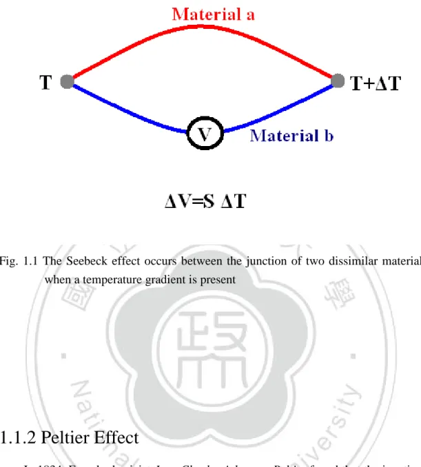
(12) 1.1 Thermoelectric Properties 1.1.1 Seebeck Effect In 1821, German-Estonian physicist Thomas Johann Seebeck found the effect which is the conversion of temperature differences directly into electricity called Seebeck effect. The Seebeck effect, or Seebeck coefficient, S, describes the establishment of a voltage gradient across a material in response to a temperature gradient (Fig.1.1): Sab =. 𝑑𝑉 𝑑𝑇. 𝑉. ( ) 𝐾. (1.1). where Sabis the relative thermopower across the junction of two materials. Intuitively, the establishment of a temperature gradient implies a higher concentration of charge carriers at the cold end of the sample, which in turn corresponds to the establishment of a voltage differential across the sample. As a corollary, the sign of the Seebeck coefficient is typically negative for n-type electrical conduction, where electrons are the primary charge carriers, and positive for p-type conduction, where holes are themajority carriers.. 2.
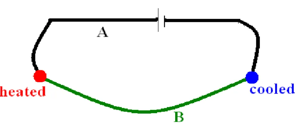
(13) Fig. 1.1 The Seebeck effect occurs between the junction of two dissimilar materials when a temperature gradient is present. 1.1.2 Peltier Effect In 1834, French physicist Jean Charles Athanase Peltier found that the junctions of dissimilar metals were heated or cooled, depending upon the direction in which an electrical current passed through them. Heat generated by current flowing in one direction was absorbed if the current was reversed. The Peltier effect is found to be proportional to the first power of the current, not to its square, as is the irreversible generation of heat caused by resistance throughout the circuit. The junction emf, πab, is known as the Peltier coefficient, is expressed as: ΠAB = -ΠBA =. 1 𝑑𝑄 𝐼 𝑑𝑡. (1.2). where dQ/dt is the rate of heat transfer at the junction, and I is the electrical current. 3.
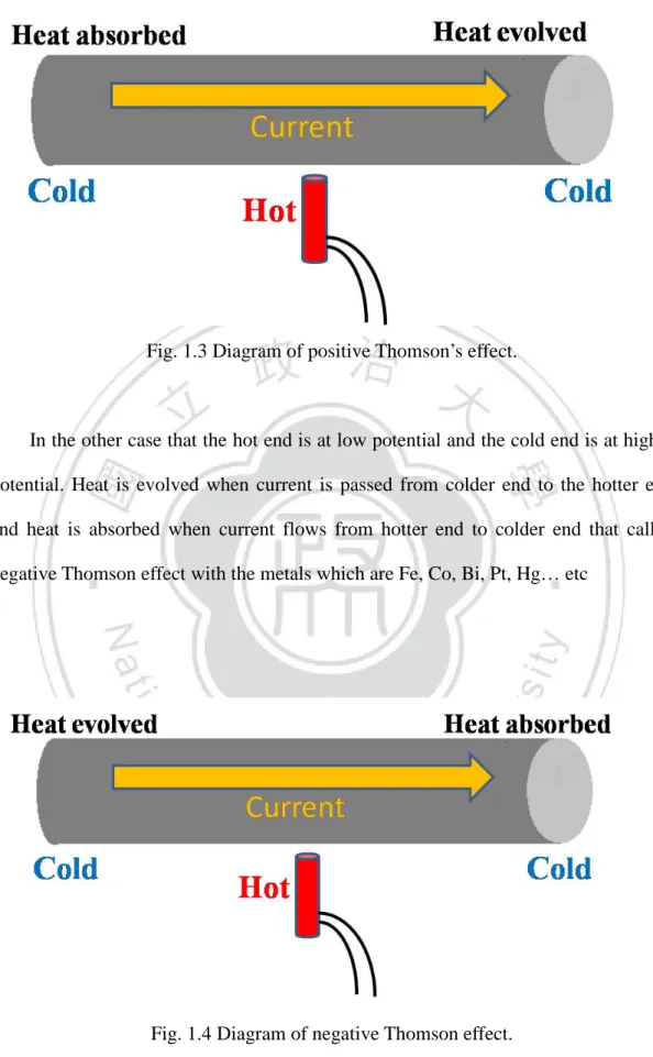
(14) ΠAB means the current from A to B and ΠBA inverse to ΠAB .The Peltier effect usually applied in the thermoelectric refrigerator.. Fig. 1.2 The Peltier effect. When an electrical current is injected, heat is expelled or absorbed at the junction between material A and B.. 1.1.3 Thomson Effect When a current flows through an unequally heated metal, there is an absorption or evolution of heat in the body of the metal that is Thomson effect. The metals which show positive Thomson’s effect are Cu, Sn, Ag, Cd, Zn… etc, it is found that hot end is at high potential and cold end is at low potential. Heat is evolved when current is passed from hotter end to the colder end and heat is absorbed when current is passed from colder end to hotter end.. 4.
(15) Fig. 1.3 Diagram of positive Thomson’s effect.. In the other case that the hot end is at low potential and the cold end is at higher potential. Heat is evolved when current is passed from colder end to the hotter end and heat is absorbed when current flows from hotter end to colder end that called negative Thomson effect with the metals which are Fe, Co, Bi, Pt, Hg… etc. Fig. 1.4 Diagram of negative Thomson effect.. The Thomson effect states that in the absence of Joule heating, the heat gained or 5.
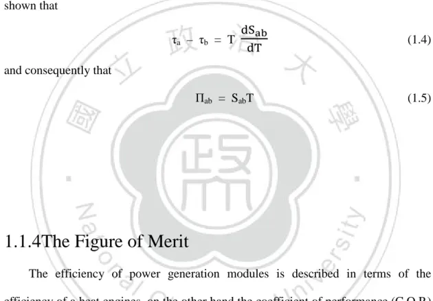
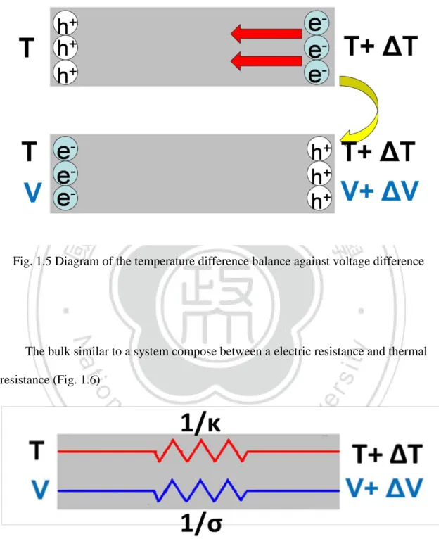
(16) lost is given by dQ ds. = τ I. dT. (1.3). ds. where s is a spatial coordinate, I is the electrical current, T is the temperature, Q is the heat, and τ is the Thomson coefficient. It should be noted that while the Seebeck and Peltier coefficients describe heat transfer in a system of two materials, the Thompson effect describes heat flow in a single material. From the Thomson effect, it can be shown that τa – τb = T and consequently that. dSab. (1.4). dT. Пab = SabT. (1.5). 1.1.4The Figure of Merit The efficiency of power generation modules is described in terms of the efficiency of a heat engines, on the other hand the coefficient of performance (C.O.P.) is characterized for the efficiency of refrigeration modules. In similar case, it is possible to relate the expressions describing the efficiency to a parameter that contains the relevant thermal, electrical, and thermoelectric parameters, the tuning of which is at the center of research into thermoelectric materials. The relation of this parameter, the “Figure of Merit” to the coefficient of performance and heat engine efficiency is outlined here. Figure of Merit (Z) =. S2. 𝛋ρ. Apply a temperature differential to a bulk material and the electrons get the 6. (1.6).
(17) energy from the hot side to cold side arrived to balance (Fig.1.5).. Fig. 1.5 Diagram of the temperature difference balance against voltage difference. The bulk similar to a system compose between a electric resistance and thermal resistance (Fig. 1.6). Fig. 1.6 Diagram of electrical circuit The coefficient of performance, Φ, is related to the total heat flow, dQ/dt, and the power input, P, as follows: Φ =. 1 dQ. P dt 7. 1.7).
(18) Here, Q is the sum of heat flow due to the thermal conductance of the material, Qκ,the Peltier heat flow, QП, and the heat loss due to Joule heating, QI. That is, Q = QK + QΠ + QI where, K is thermal conductance QK= -KΔT. (1.8). QΠ= IST. (1.9). QI = - σ(ΔV)2. (1.10). The power supplied to the device is giving by Joule expression: P = I2R. (1.11). Therefore the C.O.P. becomes Φ=. Q P. =. −KΔT+IST−σ(ΔV)2 I2 R. (1.12). By differential calculation dΦ/dt = 0 can get the maxima value of I IMax =. KΔT+σ(ΔV)2 ST. =. 2KΔT ST. (1.13). Cause balance between thermal and electrical. Then, replace IMax back into equation (1.12) and simpler the formula. ΦMax(IMax) =. S2 T2 −4ΔT RK. 4ΔT. (1.14). In equation (1.14) thermal conductance K and resistance R depend on dimensions of sample. Hence, using the thermal conductivity κ and the electrical resistivity ρ to substitute for its. It is customary to define a new quantity, the figure of merit, Z, as. Z =. S2. 𝛋ρ. (1.15). The dimension of Z is T-1, hence, let this value multiply to T defined the newcoefficient ZT that becomes dimensionless shown as.. 8.
(19) S2 T. ZT =. S2 σT. (1.16). ZT2 −4ΔT. (1.17). 𝛋ρ. Thus the C.O.P. becomes. ΦMax=. =. 𝛋. 4ΔT. The efficiency of a heat engine is given by the well-known formula: η=. W. where,. dQ/dt. W = IΔVSeebeck – IΔVR = ISΔT – σ(ΔV)2 Q = κΔT + IST –σ(ΔV)2. (1.18) (1.19). Then the transformational efficiency of electrical energy as: η=. ISΔT –σ(ΔV)2. (1.20). κΔT + IST –σ(ΔV)2. It also has the maxima n\value with I’Max through derivative of η equal to zero. After some simplification, that is I’Max =. SΔT. S2 ρ�1+( )T+1 ρκ. =. SΔT. ρ�1+(ZT)T+1. (1.21). Replace I’Max into eq. [1.20] and simplify it that is reducing to η=. TH −TC √1−ZT−1 TH √1+ZT+ TC. TH. ,. where T =. TH +TC 2. (1.22). When Z→∞, the expression for the efficiency given in eq. (1.22) approaches the Carnot limit. The calculations showing the relationship of theoretical ZT values to the relative Carnot efficiency and the C.O.P. have revealed an interesting trend.[2] It was shown that a ZT in the range of 2-3 corresponds to a Carnot efficiency of about 40-50% in the power generation scheme or a C.O.P. of 2-3 in the refrigeration configuration.[1] 9.
(20) Fig. 1.7 Figure of merit, ZT, as a function of relative Carnot efficiency. [2].. Fig. 1.8 ZT is a function of coefficient of performance at various temperatures. [2].. 10.
(21) 1.2 Crystal Growth Methods 1.2.1 Bridgman–Stockbarger Method The methods named by Harvard physicist Percy Williams Bridgman and MIT physicist Donald C involve heating polycrystalline material above its melting point and slowly cooling it from one end of its container, where a seed crystal is located. The process can be carried out in a horizontal or vertical geometry. The difference between the Bridgman technique and Stockbarger technique is subtle: while a temperature gradient is already in place for the Bridgman technique, the Stockbarger technique requires pulling the boat through a temperature gradient to grow the desiredsingle crystal.. Fig. 1.9 Diagram of Bridgman method for crystal growth. 11.
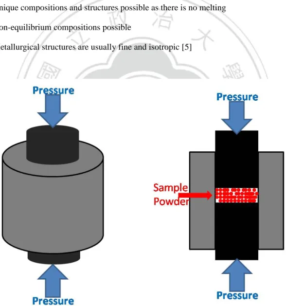
(22) Fig.1.10 Diagram of Stockbarger technique for crystal growth. 1.2.2 Powder Metallurgy Method The powder metallurgy process generally consists of four basic steps: (1) Powder manufacture (2) Powder blending (3) Compacting (4) Sintering or Annealing The powder metallurgy existed in Egypt as early as 3000 B.C. It can improve the compaction and the material properties through the sintering process. The technical 12.
(23) and commercial advantages of producing parts from powder canbe summarized as below: Production to near net shape Few or no secondary operations High material utilization from low levels of ‘in process scrap’ Homogeneous powder and hence part, chemical composition due to absence of gross solidification segregation and uniform pre-alloyed powder particle composition Unique compositions and structures possible as there is no melting Non-equilibrium compositions possible Metallurgical structures are usually fine and isotropic [5]. Fig. 1.11 Diagram of the compacted process of powder metallurgy method. 1.3 Nomenclature 13.
(24) Symbol. Units. Description. A L R ρ. m2 m Ohm(Ω) uOhm-m(μΩ-m) 𝛍𝐕 𝐊 𝐦𝐦𝟐 𝐬 𝐠 𝐜𝐦𝟑 𝐖 𝐦𝐊 K K-1. Area Length Resistance Resistivity. S D d κ T Z. 14. Seebeck coefficient Thermal diffusivity Density Thermal Conductivity Temperature Figure of Merit.
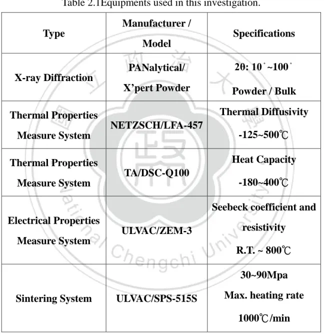
(25) Chapter 2 Experimental Techniques 2.1 Equipments The equipment used in this investigation is listed in Table 2.1.. Table 2.1Equipments used in this investigation. Manufacturer / Type. Specifications Model PANalytical/. 2θ: 10。~100。. X’pert Powder. Powder / Bulk. X-ray Diffraction Thermal Diffusivity. Thermal Properties NETZSCH/LFA-457 Measure System. -125~500℃. Thermal Properties. Heat Capacity TA/DSC-Q100. Measure System. -180~400℃ Seebeck coefficient and. Electrical Properties ULVAC/ZEM-3 Measure System. resistivity R.T. ~ 800℃ 30~90Mpa. Sintering System. ULVAC/SPS-515S. Max. heating rate 1000℃/min. 15.
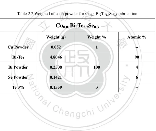
(26) 2.2 Bulk Fabrication Prepare the powder with the correct ratio (table2.2, 2.3) in dry box and put into the smaller tube (10 x 12 x 60 mm) after blending, then sealed in the bigger quartz tube (13 x 16 x 20 mm) under the pressure below 10-5 torr (Fig.2.1). Put the quartz tube with the sample powder into furnace to fabricate (Fig.2.2) with the annealing pattern (Fig.2.3, 2.4).. Table 2.2 Weighed of each powder for Cu0.01Bi2Te2.7Se0.3 fabrication. Cu0.01Bi2Te2.7Se0.3 Weight (g). Weight %. Atomic %. Cu Powder. 0.052. 1. --. Bi2Te3. 4.8046. Bi Powder. 0.2508. Se Powder. 0.1421. Te 3%. 0.1559. 90 100. 4 6. 3. 16. --.
(27) Table 2.3 Weighed of each powder for BixSb2-xTe3 (x=0.4, 0.45, 0.5 and 0.6) fabrication. Bi0.4Sb1.6Te3 Weight (g) Bi2Te3. Weight %. 1.1647. Atomic % 20. 100 Sb2Te3. 3.6439. Te 3%. 0.1443. 80 3. --. Weight %. Atomic %. Bi0.45Sb1.55Te3 Weight (g) Bi2Te3. 1.2425. Sb2Te3. 3.3481. Te 3%. 0.1376. 22.5 100 77.5 3. --. Weight %. Atomic %. Bi0.5Sb1.5Te3 Weight (g) Bi2Te3. 1.922. 25 100. Sb2Te3. 4.771. Te 3%. 0.208. 75 3. --. Weight %. Atomic %. Bi0.6Sb1.4Te3 Weight (g) Bi2Te3. 1.6566. Sb2Te3. 3.0234. Te 3%. 0.1414. 30 100 70 3. 17. --.
(28) Fig.2.1 Diagram of quartz tube sealing. Fig. 2.2 Left: diagram of sample melting in furnace; Right: real photo.. 18.
(29) 1200. Keep at 1050 10hrs 1050 to 650 12hrs. 900. T( OC). R.T to 1050 16hrs. 600 Back to R.T.. 300. 0 0. 10. 20. 30. 40. 50. Hours Fig. 2.3 Anneal pattern for Cu0.01Bi2Te2.7Se0.3. 900. 600. O. T ( C). Keep at 750 12hrs. R.T to 750 12hrs. 750 to 630 3hrs 630 to 560 9hrs 560 to R.T. 8hrs. 300. 0. 0. 10. 20. 30. 40. Hours Fig. 2.4 Anneal pattern for BixSb1-xTe3 (x=0.4, 0.45, 0.5 and 0.6) 19.
(30) 2.3 X-ray Diffraction X-ray diffraction (XRD) is a universal method to analysis about the chemical composition and crystallographic structure of natural and manufactured materials. After the bulk fabrication, confirming the phase structure by it. According to the Bragg’s law (Fig.2.5): 2dsinθ = nλ. (2.1). where, d is the distance between two nearest layers of atoms, λ is the wavelength of indicated light and θ is the angle between indicated light and layer.. Fig.2.5 Bragg’s diffraction Although Bragg’s law was used to explain the interference pattern of X-rays scattered by crystals, diffraction has been developed to study the structure of all states of matter with any beam, e.g., ions, electrons, neutrons, and protons, with a wavelength similar to the distance between the atomic or molecular structures ofinterest.. 20.
(31) Fig.2.6 measured parts of XRD, left: diagram; right: real photo. When indicated X-ray’s optical path difference satisfied with Bragg’s law that reflected light generate the constructiveinterference. Take the signals compared to reference from the database to confirm the phase structure.. 2.4 Thermal Properties Measure Systems 2.4.1 LFA 457– Thermal Diffusivity The front side of a plane parallel solid sample is heated by a short laser pulse. The heat induced propagates through the sample and causes a temperature increase on the rear surface. This temperature rise is measured versus time using an infrared detector. The thermal diffusivity,D, and in many cases also the specific heat, Cp, can 21.
(32) be ascertained using the measured signal. If the density,d, is known, the thermal conductivity ,κ, can be determined κ(T) = D(T)Cp(T)d(T). (2.2). The Sample is prepared with thickness t, then thermal diffusivity, D, can be measured by LFA457 follow the formula: D = 0.1388. t2. τ0.5. (2.3). where, τ0.5 is the half-time of IR-detector detect the signal from minima to maxima.. (a). Fig. 2.7 Diagram of laser excited in LFA. 22.
(33) Fig. 2.8 Diagram of LFA’s holder. 2.4.2 DSC Q100 – Specific Heat Differential Scanning Calorimeters (DSC) measures temperatures and heat flows associated with thermal transitions in a material. Common usage includes investigation, selection, comparison and end-use performance evaluation of materials in research, quality control and production applications. Properties measured by TA Instruments’ DSC techniques include glass transitions, “cold” crystallization, phase changes, melting, crystallization, product stability, cure kinetics, and oxidative stability. In this study, prepare the sample which is already measure the weight, next seal in the Aluminum dish (Fig.2.9).. 23.
(34) Fig. 2.9 Diagram of sealing sample in the aluminum dish then, put the sample which is already sealing into the DSC chamber to measure specific heat by heat flow between reference platform and sample platform, according to: ΔH = mCpΔT. (2.4). Fig.2.10 The tools in the DSC chamber, a) diagram of measured parts; b) real photo; c) real photo with reference (up) and sample (down).. 24.
(35) 2.4.3 Density According to the Archimedes principle which is shown any floating object displaces its own weight of fluid; any object, wholly or partially immersed in a fluid, is buoyed up by a force equal to the weight of the fluid displaced by the object. F = Volume of sample x density of fluid Therefore, the density of sample can measure by it. Take a beaker which has about 15cc DI water inside putting on the balance and zero it. Next, prepare an aluminum wire (10 cm length, 25 μm dia. ) connect to the sample with GE varnish (Fig.2.11L), then, hand the a part of wire let the sample sink in water and read the balance value which is the volume of sample (Fig.2.11R).. Fig. 2.11 Left: photo of connect the sample with GE vanish; Right:Diagram of density measurement 25.
(36) 2.5 Electrical Measure Systems 2.5.1 ZEM-3– Seebeck coefficient & Resistivity In this study, it can measure samples’ seebeck coefficient and electrical resistivity by ZEM-3 in the same time. Two thermocouples in the center (Fig.2.12) which can measure temperature and voltage difference and calculate the seebeck coefficient by. ΔV. S =. ΔT. (2.5). Resistance was measured by four-probe measure through relative between R and ρ calculation to obtain the resistivity. ρ =R. A L. (2.6). where, A is the cross-section of the sample, L is the distance between two central thermocouple. The measure temperature T was measured by temperature of upper and downer thermocouple,Th and Tc, therefore, T was calculated by. T=. Th +Tc 2. Fig. 2.12 Diagram of ULVAC ZEM-3 measured parts. 26. (2.7).
(37) Fig. 2.13 Real setup of ULVAC ZEM-3 measured parts. Firstly, put the sample (2 mm(W) x 2 mm (L) x h mm(H)) between upper and downer electrode with the right thermocouple distance (3, 6 or 8 mm) to attach sample(Fig.2.13). Then, measuring the I-V curve to check the contact is good or not. Secondly, first pumping for the measured chamber at -0.1 Mpa after that flow gas helium into chamber back to normal pressure next is do the second pumping over than 10 minutes to make sure the pressure below than -0.1 MPa afterwards flow the helium again to -0.09MPa be the exchange gas. Finally, set the parameter to software such as temperature range, delta T (for seebeck measurement) and sample’s scale.Thereupon, ZEM-3 will measure S and ρ automatically.. 27.
(38) 2.5.2 Hall Effect In 1879, Edwin Halldiscovered the Hall Effect which is the production of a Hall voltage across an electrical conductor, transverse to an electric current in the conductor and a magnetic field perpendicular to the current.The Hall Effect comes about due to the nature of the current in a conductor. Current consists of the movement of many small charge carriers, typically electrons and holes.If an electric current flows through a conductor in a magnetic field, the magnetic field exerts a transverse force on the moving charge carriers which tends to push them to one side of the conductor.A buildup of charge at the sides of the conductors will balance this magnetic influence, producing a measurable voltage between the two sides of the conductor which is called Hall voltage VH follow as:. VH e eIB Fm = evd B = neA, Fe = W. Fm = Fe , VH = n =. IB. edVH. IB. ned. (2.8) (2.9) (2.10). where, e is a electron charge constant, I is the current, Bis the magnetic field, W is the width of the sample, d is the thickness of sample, A is the cross-section (W x d) of sample and n is the carrier concentration.. 28.
(39) Fig. 2.14 Diagram of Hall effect measurement.. In this study, it will discuss the relative between thermoelectric properties and carrier concentration. So, measure the concentration by PPMS with the magnetic field 9T and -9T to modify the VH wire connection non-straight (can’t measure at the same cross-section). So, the Hall voltage is getting by. VH =. V �with 9T�−VH(with−9T) � H � 2. (2.11). 2.6 Spark Plasma Sintering The SPS process features a very high thermal efficiency because of the direct heating of the sintering mold and stacked powder materials by large spark pulse 29.
(40) current. It can easily consolidate a homogeneous, high-quality sintered compact because of the uniform heating, surface purification and activation made possible by dispersing the spark point.The theory behind it is that there is a high-temperature or high-energy plasma that is generated between the gaps of the powder materials; materials can be metals, inter-metallic, ceramics, composites and polymers Using a DC pulse as the electrical current, spark plasma, spark impact pressure, joule heating, and an electrical field diffusion effect would be created.[3] Through various experiments it has been found that in order to design the mechanical properties of new material, controlling the grain size and its distribution, amount of distribution and other is pinnacle. Fabricate the sample’s powders which are three kinds of powders. Firstly, it is pure bulk powders whichwere fabricatedthrough ball milling with the condition, 500 rpm for 30 minutes and pause 10 minutes repeat 20 times. Secondly,those were fabricated pure nanoparticles by hydrothermal method from Dr. Chang in M.K.Wu’s lab. Finally, mix the bulk powders and nanoparticles with thedesignated ratio. Next, load the sample’ powder into mold. Put the graphite mold which has the powder inside into Spark Plasma Sintering (SPS), afterwards pump SPS chamber below 6 Pa. Afterwards, sinter the powder to ingot with adaptive conditions (Table2.4).. 30.
(41) Fig. 2.15 Diagram of spark plasma sintering ON-OFF pulsed current path. Fig. 2.16 Pulsed current flow through powder particles 31.
(42) Table 2.4 SPS conditions for every sample in this study Sintering Sample. Pressure. Heating. Sintering. (Mpa). Rate (K/min). Time (min). 400. 50. 50. 5. 400. 50. 50. 5. Temperature (℃). Cu0.01Bi2Te2.7Se0.3 Bulk Powder Nanoparticles Bulk Powder (BP)+ 10 wt% NPs BP+20 wt% NPs BP+30 wt% NPs BP Bi0.45Sb1.55Te3 BP. Bi0.5Sb1.5Te3. 32.
(43) Chapter 3 Results and Discussions 3.1 Cu0.01Bi2Te2.7Se0.3 Nanocomposites 3.1.1 Analysis The. nanocomposites. presented. in. this. study. were. prepared. using. Cu0.01Bi2Te2.7Se0.3 n-type bismuth telluride based material cause that cause that has the evidence to show the Bi2Te2.7Se0.3 doping around 1 % Cu can reduce the Electrical resistivity.[7][8]. The composite microstructure and composition, as well as the effects of the nanoparticles on the thermal and electrical transport properties are presented below, with a focus on the effect of the nanoparticles on the thermoelectric efficiency of the composite. After Bridgman growth, the bulk and powders which are from ball milling were confirmed by powder x-ray diffraction (XRD) (Fig.3.1), and the particle size and morphology. was. found. by. scanning. electron. microscopy(SEM). to. be. spherical-irregular, with sizes from 20 nm to 5 μm (Fig. 3.3) and confirm the atomic percentage by SEM-EDX (Fig.3.2). From the Fig.3.2 it doesn’t find Cu signal that the reason is maybe from the rare doping is difficult to detect by EDS resolution. Compare with Fig.3.4, 3.5 and 3.6 that the amounts of nanoparticle increase by the doping percentage obviously.. 33.
(44) (0 1 20). (1 1 15). (0 2 10). (2 0 5). (0 1 13). (0 1 11). (1 1 0). (1 0 10). (1 0 1). (0 0 6). Intensity (a.u.). (0 1 5). Cu0.01Bi2Te2.7Se0.3 Bulk Powder Cu0.01Bi2Te2.7Se0.3 NPs. 20. 30. 40. 50. 60. 70. 2θ (degree) Fig.3.1 X-ray diffraction pattern of Cu0.01Bi2Te2.7Se0.3 bulk powder and nanoparticles. Fig.3.2 EDX of Cu0.01Bi2Te2.7Se0.3 NPs to show the atomic percentage.. 34.
(45) Fig.3.3 SEM images of Cu0.01Bi2Te2.7Se0.3 nanoparticles prepared by hydrothermal a) significantly smaller grain sizes b) Close view of portion from (a), nanopaticles were observed in white region. 35.
(46) Fig.3.4 SEM images of Cu0.01Bi2Te2.7Se0.3 nanocomposite 10 wt% prepared by ball milling, hydrothermal and SPS. A) Significantly smaller grain sizes b) Close view of portion from (a). 36.
(47) Fig.3.5 SEM images of Cu0.01Bi2Te2.7Se0.3 nanocomposite 20 wt% prepared by ball milling, hydrothermal and SPS. A) Significantly smaller grain sizes b) Close view of portion from (a). 37.
(48) Fig.3.6 SEM images of Cu0.01Bi2Te2.7Se0.3 nanocomposite 30 wt% prepared by ball milling, hydrothermal and SPS. A) Significantly smaller grain sizes b) Close view of portion from (a).. 38.
(49) 3.1.2 Thermal properties Thermal properties are including thermal diffusivity D, specific heat Cp, and density d, and the thermal conductivity κ relative with D, Cp and d, follow as: κ= D x Cp x d. (3.1). D (mm2/s). 1.0. 0.8. NC 10 % NC 20 % Bulk NPs NC 30 %. 0.6. 0.4. 300. 350. 400 T (K). 450. 500. Fig.3.7 Thermal diffusivity versus temperature of n-type Cu0.01Bi2Te2.7Se0.3. According to the Debye model which is a method developed by Peter Debye in 1912 that is shown about the specific heat low temperature and high temperature limitation as following formula. T. D x3 T TD = 9T ( )3 ∫ T x dx = 3TD3 0 e −1 T NK TD. U. (3.2). Where, U is energy, NK is, TDis the Debye temperature and D3 is the third Debye function. Then, differentiating with respect to T, it will show the dimensionless heat capacity. 39.
(50) T. D x 4 ex T = 9 ( )3 ∫ T x dx 0 (e −1)2 NK TD. Cv. (3.3). This formula treats the Debye model at all temperature.. In low temperature limit, the temperature of a Debye solid is said to be low if T << TD, the (eq.) can simplify leading to Cv. NK. ~ 9. T. ∞. ( )3 ∫0 TD. x4 ex x. (e −1). 2 dx =. 12π4 5. It shown the specific is directly proportional to T3.. T. ( )3 TD. (3.4). For high temperature limit, the temperature of a Debye solid is said to be low if T >> TD, using the ex-1 ~ x , if ∣x∣<< 1 T. T 3 TD x4 =9 ( ) ∫ dx = 0 x2 NK TD Cv. 3. (3.5). This is the Dulong–Petit law, and is fairly accurate although it does not take into account anharmonicity, which causes the heat capacity to rise further. The total heat capacity of the solid, if it is a conductor or semiconductor, may also contain a non-negligible contribution from the electrons. It shows the specific heat is constant closely when the temperature over than Debye temperature that has a lot of experiments show room temperature is already over than TD. And this matrix material is just the Bi2Te3 rare doping. So, it can assume the specific heat is a constant. In this study, it can use 0.2 which is the specific heat of Bi2Te3to be the Cp when the temperature over than room temperature.. 40.
(51) Table3.1 Density of all Cu0.01Bi2Te2.7Se0.3 samples in this study.. Density (g/cm3). Bulk. Nanoparticles 100 % NPs ingot. Nanocomposite 10 wt% NPs doped. 20 wt%. 30 %. 7.7278. 6.4107. 7.5864. 7.4642. 7.1243. According to eq. [2.2],κ can be calculated by multiply D, C and d.. 1.8. κ (W/m-K). 1.5. NC 20 % Bulk NC 10 % NC 30 % Bulk ref.[7] NPs. 1.2. 0.9. 0.6. 300. 350. 400. 450. 500. T(K) Fig.3.8 Thermal conductivity of Cu0.01Bi2Te2.7Se0.3 bulk, NPs, NC 10% 20% and 30% versus temperature. From the Fig.3.8, it can be observed the thermal conductivity of nanoprticles lower than bulk obviously when the temperature over than 420 K. And the result 10 wt-% nanoparticle doped is similar with the bulk powder. Although increasing the doped percentage to 20% that has the largest κ. When doping more nanoparticles to 41.
(52) 30% which has the smallest thermal conductivity obviously. So, it will shows a result that the doped ratio needs over than 20 wt% can improve the thermal properties for Cu0.01Bi2Te2.7Se0.3.. 3.1.3Electrical properties Electrical resistivity (also known as resistivity, specific electrical resistance, or volume resistivity) is a measure of how strongly a material opposes the flow of electric current. A low resistivity indicates a material that readily allows the movement of electric charge. In the definition, the resistivity show as: E ρ = J. (3.6). where, E is the electrical field and J is current density.. In this study, the resistance is. calculated through resistance measure with four-probe measure by ZEM-3. ρ=R. A L. (3.7). Fig.3.9 shows the electrical resistivity vs. temperature data for this series. The curvature of the trend for each different Cu0.01Bi2Te2.7Se0.3 shows change. It shows the resistivity of nanoparticles ingot lower than bulk about 100 % at 330K, and the composite structure lower than nanoingot and bulk around 70 % and 170 %. This reduction was caused mainly by the presence of nanostructured regions existing within the samples and through the SPS process can maintain the resistivity even reduction.. 42.
(53) Bulk NPs NC 10 % NC 20 % NC 30 % Bulk ref.[7]. ρ (µΩ-m). 45. 30. 15 300. 350. 400. 450. 500. T (K) Fig.3.9 Electrical resistivity of Cu0.01Bi2Te2.7Se0.3 materials versus temperature. Fig.3.10 shows the Seebeck coefficient vs. temperature data for this series. The curvature of the trend for each different Cu0.01Bi2Te2.7Se0.3 shows change, and the Seebeck coefficient of the nanocomposites have a mean value about -168 ± 2 μV/K at 430 K, reduction in magnitude of approximately 14 μV/K and growth in magnitude of approximately 28μV/K compared to the commercial bulk and pure nanoparticles ingot.. 43.
(54) S (µV/K). -50 NPs Bulk ref.[7] NC 20 % NC 30 % NC 10 % Bulk. -100. -150. -200. 300. 350. 400. 450. 500. T (K) Fig.3.10 Seebeck coefficient of Cu0.01Bi2Te2.7Se0.3 materials versus temperature. 3.1.4 Figure of Merit From Fig.3.11, getting the best ZT value is 0.74 at 430K by Cu0.01Bi2Te2.7Se0.3 nanocomposite with 30 wt% doped. And the each nanocomposite has the better thermoelectric properties than bulk and nanoingot. So, it can benefit the thermoelectric properties about 100% by nanocomposite. This enhancement was caused mainly by the presence of nanostructured regions existing within the samples lowered thermal conductivity due to the significant number of grain boundaries, short phonon mean free path and lattice mismatch.. 44.
(55) Figure of merit (ZT). 1.2. 0.8. Bulk ref.[7] NC 30 % NC 10 % NC 20 % Bulk NPs. 0.4. 0.0. 300. 350. 400. 450. 500. T (K) Fig.3.11ZT value of Cu0.01Bi2Te2.7Se0.3 materials versus temperature. 45.
(56) 3.2 BixSb2-xTe3 (x=0.4, 0.45, 0.5 and 0.6) 3.2.1 Analysis In normally, the x=0.5 is a famous TE material for sale. But that has a investigation to show the x=0.45 is better than 0.5. [9][10] The samples presented in this study were prepared using BixSb2-xTe3 (x=0.4, 0.45, 0.5 and 0.6) p-type bismuth telluride based material. After Bridgman growth, the ingots were confirmed by XRD (Fig.3.12), and Fig.3.13, 3.14, 3.15 and 3.16 shown in relative ratios that are consistent with the composition of the matrix material by SEM-EDX. The EDX has resolute limitation around 3-5%, so rare doped is difficult to different. According to analysis data by. 20. 30. 40. 60. (0 1 20) (1 2 5). (1 0 19). (0 1 17). (2 0 5). 50. (0 0 18). (1 0 10) (0 1 11) (1 1 10) (0 0 15) (1 1 6). x=0.60 ingot x=0.50 ingot x=0.45 ingot x=0.40 ingot. (0 1 8). (0 0 9). (0 0 6). Intensity (a.u.). (0 1 5). EDX, it shows the relative ratios are close to setup at beginning.. 70. 2θ (degree) Fig.3.12 X-ray diffraction pattern of BixSb2-xTe3 ingots(x=0.4, 0.45, 0.5, 0.6). 46.
(57) Fig.3.13 EDX of Bi0.4Sb1.6Te3 to show the atomic percentage.. Fig.3.14 EDX of Bi0.45Sb1.55Te3 to show the atomic percentage 47.
(58) Fig.3.15 EDX of Bi0.5Sb1.5Te3 to show the atomic percentage. Fig.3.16 EDX of Bi0.6Sb1.4Te3 to show the atomic percentage 48.
(59) 3.2.2 Thermal properties Thermal properties are including thermal diffusivity D, specific heat Cp, and density d, and the thermal conductivity κ relative with D, Cp and d, follow as: κ = D x Cp x d. (3.7). According to Fig.3.17, it can find the relative thermal diffusivity, D, increase following the ratio with Bi reduction when the x below 0.5. And there have a transition when the x above 0.5 that the shape of curve is different with x=0.4, 0.45 and 0.5 obviously. Maybe it shows if x larger than 0.5 that have some physical properties are changed.. Thermal Diffusivity (mm2/s). 1.6. x=0.40 ingot x=0.60 ingot x=0.45 SPS x=0.45 ingot x=0.50 ingot x=0.50 SPS. 1.4 1.2 1.0 0.8 300. 350. 400. 450. 500. T (K) Fig.3.17 Thermal diffusivity of p-type BixSb2-xTe3 versus temperature. According to Dulong–Petit law, the specific heat is constant closely when the temperature over than Debye temperature. Therefore, it can assume the specific heat is a constant. The specific heat of Bi0.45Sb1.55Te3 from 125 to 460 K is shown in 49.
(60) Fig.3.18a and compared with Fig.3.18b which is the data from reference[6] with x=0.5 which shows the specific heat close near to a constant around 0.23 when the temperature over than -50 ℃, then, it can assume C p is the constant 0.23 over than 300 K. Although the results of Fig.3.18a and Fig.3.18b are not closely, but, in this study, it still uses the real data to replace into Cp value.. Specific Heat (J/g oC). 0.30. Bi0.45Sb1.55Te3 powder Fitting Curve. 0.25 0.20 0.15 0.10 100. 200. 300. 400. 500. T (K) Fig.3.18 a) The specific heat of Bi0.45Sb1.55Te3 versus temperature b) Reference of Bi0.5Sb1.5Te3 [6]. The density can be measured by Archimedes principle. From the table3.2, it show the density and the ratio of Bi element are direct proportion obviously, because the mass of Bi is heavier than Sb. For x=0.5 SPS composite about 88 % compare to ingot, but when x=0.45 the SPS composite just 77 % with the same sintering condition. 50.
(61) Table3.2 Density of every BixSb2-xTe3 samples Ingot. x=0.4. x=0.45. x=0.5. x=0.6. 6.468. 6.643. 6.748. 6.897. x=0.45. x=0.5. 5.126. 5.925. Density (g/cm3) SPS pellet Density (g/cm3). Following eq. (2.2), κ can be calculated by multiply D, C and d.. From the Fig.3.19, it can be observed the thermal conductivity of BixSb2-xTe3 depend on the ratio of Bi, the thermal conductivity and x value are inverse proportion when the x<0.5. Combination the results of D and κ, there are also shown if the x over than 0.5, then, the trend has a little change which is about the minimum of thermal conductivity and diffusivity were moved from 360 to 300 K. And it can be observed κ goes lower through SPS process obviously that the main reason is from the increase the phonon scattering because it has more boundaries in the SPS composites.. 51.
(62) 2.8. x=0.60 ingot x=0.40 ingot x=0.45 ingot x=0.50 ingot x=0.45 SPS x=0.50 SPS. κ (W/m-K). 2.4 2.0 1.6 1.2 0.8. 300. 350. 400. 450. 500. T (K) Fig.3.19 Thermal conductivity of BixSb2-xTe3 bulk, x=0.4, 0.45, 0.5 and 0.6 versus temperature. 3.2.3Electrical properties Fig.3.20 shows the electrical resistivity vs. temperature data for this series. The curvature of the trend for each different BixSb2-xTe3 shows change. In normally, the SPS process can maintain or reduce the resistivity and reduce the thermal conductivity. Compare between Fig.3.19 and Fig.3.20, Bi0.5Sb1.5Te3’s result shows that decrease the κ and maintain the resistivity through SPS fabrication. Next, in the Bi0.45Sb1.55Te3’s data, even thermal conductivity is reduced, but the resistivity larger about 10 times. 52.
(63) The mainly reason maybe from the density which is lower than x=0.5 about 13.5 %. The effect likes impurity diffusion in the sample, then the electrons passing difficulty. Therefore, ρ is increase several times. Next, it focus on the curvatures which are differenced to two shapes, the first is x=0.4 and 0.4 that trend is linear line similar and the second is x=0.45 SPS, 0.5 and 0.6 the shape are curve.. 120. ρ (µΩ-m). 100 x=0.45 SPS x=0.60 ingot x=0.40 ingot x=0.50 SPS x=0.50 ingot x=0.45 ingot. 80 60 40 20 300. 350. 400. 450. 500. T (K) Fig.3.20 Electrical resistivity of BixSb2-xTe3 materials versus temperature. From Fig.3.21 shows the Seebeck coefficient vs. temperature data for this series. The curvature of the trend for each different BixSb2-xTe3 shows change, and the Seebeck coefficient at 320 K of each x valued have a range about from 180 to 275 μV/ K, the samples were fabricated by SPS process which the S are higher than original ingots in evidence. In physics rule, the S and ρare direct proportion and through to compare the results of the x=0.45 and 0.5 can observe it obviously. The ingots’ S is not sensitive with the amount of Bi, but the curvature of x=0.4 is different 53.
(64) to others.. S (µV/K). 280 x=0.50 SPS x=0.45 SPS x=0.50 ingot x=0.60 ingot x=0.45 ingot x=0.40 ingot. 240. 200. 160 300. 350. 400. 450. 500. T (K) Fig.3.21 Seebeck coefficient of BixSb2-xTe3 materials versus temperature. By Fig.3.22, it shows the carrier concentration of each sample which can explain the reason of the lowest resistivity from Bi0.45Sb1.55Te3 directly. From this result that it can harvest a conclusion that the x=0.45 ingot’s concentration has changed after SPS process. In general, the resistivity is inverse proportion to carrier concentration. Therefore, it compares between Fig.3.20 and 3.22 and the results are also following ρ ∝ 1/n . It is can explain why the x=0.45 ingot has the lowest resistivity because by the highest carrier concentration.. 54.
(65) Carrier Concentration (1021/m3). 25 x=0.45 ingot x=0.50 ingot x=0.60 ingot x=0.40 ingot x=0.45 SPS. 20 15 10 5 0 320. 325. 330. 335. 340. T (K) Fig.3.22 The carrier concentrations of BixSb2-xTe3 materials from 320 to 340 K.. 3.2.4Figure of Merit In this study, the best ZT value1.46 is obtained at 300K by x=0.45 ingot. Firstly, it focuses on x=0.5 which the composite was fabricated through SPS technique can enhance the ZT valuearound 50% from 0.72 to 1.15 at 340K.However, in the other case that the ZT of x=0.45 compositewas decreased after SPS process. Although the result is with lower thermal conductivity and higher Seebeck coefficient, but the mainly problem is from the 10 times larger electrical resistivity, therefore, the figure of merit is smaller around 8 times than the original ingot. Compare the results S and ρ that have not a lot differences between x=0.4, 0.5 and 0.6. And the ZT values of x=0.4 55.
(66) and 0.6 are smaller than x=0.5 that the main reason is from thermal conductivity. The best ZT is x=0.45 that caused by the lowest electrical resistivity. Then, it discuss between Fig.3.22 and 3.23 that show the result is the sample has the higher ZT value with the higher carrier concentration.. x=0.45 ingot x=0.50 SPS x=0.50 ingot x=0.40 ingot x=0.60 ingot x=0.45 SPS. Figure of Merit (ZT). 1.5. 1.0. 0.5. 0.0. 300. 350. 400. 450. 500. T (K) Fig.3.23ZT value of BixSb2-xTe3 (x=0.4, 0.45, 0.5 and 0.6) materials versus temperature. 56.
(67) Chapter 4 Conclusions This study provides at the first investigation of the effects of nanomaterials upon the thermal and electrical transport properties of nanocomposites formed using favorable thermoelectric(TE) materials as a matrix. The nanocomposites studied herein are also of value for investigating the viability of the spark plasma sintering(SPS) technique for producing such composites, as well as being of benefit for studying viable techniques of nanoparticle growth. While the end results have in most cases not been the formation of nanocomposites that have figures of merit that surpass the bulk materials, the effects of the nanomaterials upon the electrical and thermal properties nevertheless help illuminate interesting new directions for thermoelectric research of nanocomposites. The ZT value is enhanced around 100% through 30 wt% nanoparticles doping. If the bulk material can fabricate achieving to commercial value about 0.9 like as ref.[7], afterwards, use the nanocomposited method. The ZT is expected to exceed 1.2at T >400 K. For the other investigation which discussed the effects about BixSb2-xTe3 with the different ratios of Bi doping. Firstly, the thermal conductivity has change following the Bi amounts. It shows when the x<0.5, the κ and x are inverse proportion. When the x above 0.5, in this study with x=0.6, the κ is enlarge to near with the result of x=0.4 and the shape of curve has changed. Next, that discuss to electric properties, in general, the materials’ S and ρ are direct proportion. And the results are following this rule. In the end, it obtain the best ZT~1.5 at 300 K by x=0.45 ingot in this study caused by the lowest electrical resistivity and proving the SPS process can effectively enhance the TE properties by the case of x=0.5 and the first investigation. The carrier concentrations of x=0.45 and x=0.5 SPS are larger than 1022/m3 which have the ZT value large than 1. 57.
(68) Reference [1] Nicholas Wesley Gothard, The Effects of Nanoparticle Inclusions Upon The Microstructure. and. Thermoelectric. Transport. Properties. of. Bismuth. Telluride-Based composites, Clemson University PhD thesis (2008) [2] J. Yang and T. Caillat,Thermoelectric Materials for Space and Automotive Power Generation, “MRS Bulletin 31, 224 (2006) [3] M. Tokita, Mechanism of Spark Plasma Sintering, Sumitomo Coal Mining Company Ltd, Japan [4] C.L. Chen, Thermoelectricity of (Bi,Sb)2Te3 nanomaterial and photothermal properties of Au nanorods, National Taiwan Normal University PhD thesis (2009) [5] G. Greetham, Powder Metallurgy-An Introduction [6] Scheele, American Chemical Society, Vol. 4, No. 7, 4283-4291(2010). [7] J.L. Cui,Thermoelectric properties of Cu-doped n-type(Bi2Te3)0.9-(Bi2-xCuxSe3)0.1 (x =0–0.2) alloys, Journal of Solid State Chemistry, 180, 3583–3587(2007) [8] Sin-Shien Lin, et al., Journal of applide physics, 110, 093707 (2011) [9] Jun Jiang, et al., Scripta Materialia 52, 347–351 (2005) [10] Chia-Jyi Liu, et al., J. Mater. Chem., 22, 4825(2012). 58.
(69)
數據
+7
![Fig. 1.7 Figure of merit, ZT, as a function of relative Carnot efficiency. [2].](https://thumb-ap.123doks.com/thumbv2/9libinfo/8195153.169258/20.892.150.759.112.1041/fig-figure-merit-zt-function-relative-carnot-efficiency.webp)

相關文件
Trinity Church (also known as Trinity Wall Street) at 79 Broadway, Lower Manhattan, is a historic, active parish church in the Diocese of New York. Trinity Church is at
The purpose of this research is to study a tiling problem: Given an m × n chessboard, how many ways are there to tile the chessboard with 1 × 2 dominoes and also ”diagonal”
It has been well-known that, if △ABC is a plane triangle, then there exists a unique point P (known as the Fermat point of the triangle △ABC) in the same plane such that it
The function f (m, n) is introduced as the minimum number of lolis required in a loli field problem. We also obtained a detailed specific result of some numbers and the upper bound of
• Figure 26.26 at the right shows why it is safer to use a three-prong plug for..
• Figure 26.26 at the right shows why it is safer to use a three-prong plug for..
We compare the results of analytical and numerical studies of lattice 2D quantum gravity, where the internal quantum metric is described by random (dynamical)
strongly monotone or uniform P -function to obtain property of bounded level sets, see Proposition 3.5 of Chen and Pan (2006).. In this section, we establish that if F is either
