Received June 30, 1999; revised December 23, 1999; accepted March 7, 2000. Communicated by Kuen-Jong Lee.
* This work was supported in part by the National Science Council, Taiwan, R.O.C. under Grant NSC-88-2215-E238-002.
687
Flip-Flop Selection for Mixed Scan and Reset Design Based
on Test Generation and Structure of
Sequential Circuits
*HSING-CHUNG LIANGAND CHUNG LEN LEE+ Department of Electronic Engineering
Chang Gung University Taoyuan, Taiwan 333, R.O.C. E-mail: [email protected] +Department of Electronics Engineering
National Chiao Tung University Hsinchu, Taiwan 300, R.O.C. E-mail: [email protected]
In this paper, a novel mixed selection methodology using flip-flops for scan and reset design is proposed. The method runs test generation for a sequential circuit to obtain reachable states of flip-flops and required states for hard-to-detect faults. The circuit is also explored so as to acquire the structural connection relationship among the flip-flops. By analyzing these three sets of information, the flip-flops can be arranged in an appropriate order for mixed partial scan and reset selection. Instead of selecting the best flip-flop to revise the circuit for the next test generation, we give first priority to independent flip-flops each time in order to reduce the number of iterations. Experimental results show that this method can achieve higher testability with fewer scan/reset flip-flops than can either the scan only or the previous mixed scan/reset methods.
Keywords: partial scan, partial reset, reachable states, test generation, design for testability
1. INTRODUCTION
After decades of research, it is now generally recognized that to solve the testing problem, design for testability (DFT) must be incorporated into VLSI. For sequential circuits, scan design is the most widely used DFT method [1-32]. The full scan [3] can achieve very high testability, but it suffers from the disadvantages of excessive hardware overhead and lengthy test application time. Partial scan [4-32] and partial reset [33-36] have been consid-ered to be more practical approaches to lessen the above problems while still maintaining a certain level of testability.
For partial scan, many methods have been proposed to select the minimal number of flip-flops so as to increase the maximal possible testability. Those methods can basically be classified as follows: (1) testability-measure-oriented [4-14]; (2) structure-analysis-oriented [7, 10, 13, 15-27]; and (3) test-generation-oriented [6, 10, 14, 28-31]. Each category of methods has its advantages and disadvantages. For example, calculating the testability may
be very fast, but the measure may not be exact enough. Structural analysis is also fast, but hard-to-detect faults are not completely related to the way of circuit's connection. Test generation methods consider fault behavior directly but they take a long time or require too many iterations. Consequently, combinations of the above methods have also been consid-ered [6, 7, 10, 13, 14, 32] in the hope of finding the perfect flip-flops so as to achieve a high level of testability.
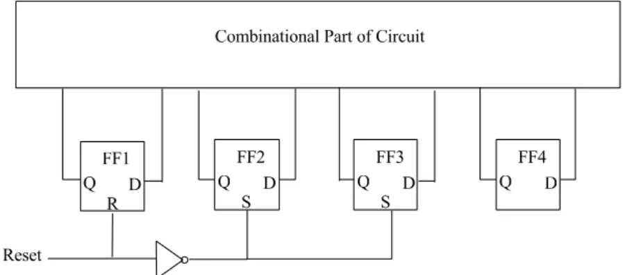
Partial reset is an appealing technique in DFT because it increases the controllability of circuits with negligible modification of selected flip-flops and fewer additional inputs compared to scan design. Fig. 1 shows an example of partial reset design. The reset flip-flops can be forced into definite states at any time during the test pattern application. Obviously, the number of valid states of the circuit can be, therefore, increased, and so can the circuit’s testability. Compared to partial scan, partial reset allows the circuit-under-test (CUT) to be tested at high speed with less test application time. The authors in [33] se-lected the reset flip-flops and their reset values by analyzing the state table of the circuit, those in [34] did so by breaking cycles and calculating the controllability of the circuit, and those in [35] did so by utilizing a cost function to conduct sensitivity analysis.
Fig. 1. An example of partial reset design. As the signal ‘Reset’ becomes 0, the outputs of flip-flops FF1, FF2, and FF3 are forced to be 0, 1, and 1, respectively.
Combinational Part of Circuit
FF1 D Q R FF2 D Q S FF3 D Q S FF4 D Q Reset
Recently, it has been proposed that partial scan and partial reset be employed together in the CUT to enjoy the advantages of both approaches [36, 37]. Through using this approach, one can improve the level of controllability while achieving the needed level of observability of the CUT by using much less hardware as compared to scan only design. These methods select reset flip-flops first and then scan flip-flops in order to improve the circuit’s testabil-ity with as few flip-flops as possible.
In this paper, a new method for selecting flip-flops for partial-scan and partial-reset design is proposed. Instead of selecting flip-flops first for reset and then for scan, we com-bine the steps to achieve better results. The method utilizes the following information to select the optimal flip-flops for partial scan and/or reset:
(1) the reachable states obtained from test pattern simulation,
(2) the fault-free states needed for excitation and propagation for hard-to-detect faults, and
By analyzing the above information, we can construct the appropriate selection se-quence for flip-flops that are to be scanned or reset. The flip-flops which are predicted to improve testability more are given first priority for selection. Because choosing only one flip-flop each time for DFT requires many iterations, especially for large circuits, we simul-taneously select those flip-flops which are independent in structure so as to reduce the required run time. Experiments on ISCAS89 [38] benchmark circuits show that the pro-posed method needs fewer flip-flops for scan or reset but achieves higher fault coverage than do the previous mixed scan/reset or scan only methods.
Section 2 describes how the three sets of information are collected. We explain how they are analyzed to guide flip-flop selection in section 3. Experimental results and conclu-sions are then given in sections 4 and 5, respectively.
2. INFORMATION FOR FLIP-FLOP SELECTION
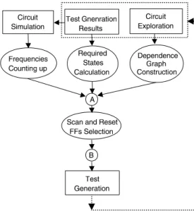
The overall process involved in this mixed scan/reset flip-flop selection approach is shown in Fig. 2. As mentioned above, information on reachable states, the fault-free states needed for excitation and propagation of hard-to-detect faults, and the structureal connec-tion relaconnec-tionships among the flip-flops, is collected first. Consequently, at the beginning, a deterministic test generator is applied to the CUT to generate test patterns for the easy-to-detect faults in the circuit while using little computation time as possible. During this test generation step, the faults that the test generator identifies as being untestable and those for which it cannot find test patterns are called hard-to-detect faults. The states required to excite and propagate these faults to primary outputs are collected during the test generation step. The test patterns obtained by the test generator are then used to simulate the circuit in order to obtain the reachable states. At the same time, the circuit is analyzed in order to construct its dependence graph [39], which describes the structural relationships among the flip-flops. After analyzing the data to guide selection of the best flip-flop(s) for scan or
Fig. 2. The overall selection process for scan and reset flip-flops.
A
B Frequencies
Counting up Circuit
Simulation Test GnenrationResults Required States Calculation Circuit Exploration Dependence Graph Construction
Scan and Reset FFs Selection
Test Generation
reset, we revise the circuit and run the test generation procedure for the subsequent sets of data. The process can be executed repeatedly until the obtained fault coverage satisfies the requirement. The details of the above data are described, respectively, in the following subsections.
2.1 Simulation for Reachable States
The reachable states are those states that can be reached from any state of a sequential machine. They represent the states that are ready for excitation and propagation of target faults for test generation. Obviously, the circuit can be much more testable if it has many valid states. Searching for all the valid states of a circuit is impractical, so we use reachable states that have been simulated based on test patterns generated using an implemented BACK[40,41]-like test generator. From these states, which are recorded in the set RS, we count up the 1 and 0 frequencies present on each flip-flop. These frequency counts indicate the difficulty involved in setting the flip-flops to be 0 and 1. The smaller the frequency, the more difficult it is to set the corresponding value. These count values, therefore, are a great aid in selecting flip-flops for partial scan/reset.
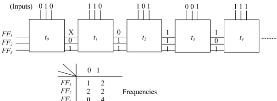
Example 1: Fig. 3 shows an example where the input patterns (010,110,101,001,111, ...) are used to simulate a circuit with three flip-flops. The reachable states obtained after this simulation is conducted are RS(FF1, FF2, and FF3) = (X01,011,111,101, ...). Then the frequencies of occurrence of 1 and 0 on these reachable state cubes are calculated. In Fig. 3, the frequencies of occurrence of 0 for FF1, FF2, and FF3 are 1, 2, and 0, respectively. This indicates that the value 0 does not occur on flip-flop FF3 until now, which implies that it is difficult for the circuit to set FF3 to be 0 during test generation.
Fig. 3. An example showing the reachable states obtained through logic simulation. On the flip-flops, ‘X’ means don’t care.
(Inputs) 0 1 1 2 2 2 0 4 FF1 FF2 FF3 0 1 0 t0 1 1 0 t1 X 0 1 1 0 1 t2 0 1 1 0 0 1 t3 1 1 1 1 1 1 t4 1 0 1 FF1 FF2 FF3 Frequencies
2.2 States Required for Excitation and Propagation for Fault Detection
To generate a test for a fault, it is necessary to excite and propagate the fault, perhaps through several time frames, to a primary output. During excitation and propagation, if it is difficult or impossible for the circuit to have the required states, then the target fault is likely to be aborted or judged untestable by the test generator. Accordingly, we will collect these needed states for hard-to-detect faults during the test generation phase in the set NS for further analysis.
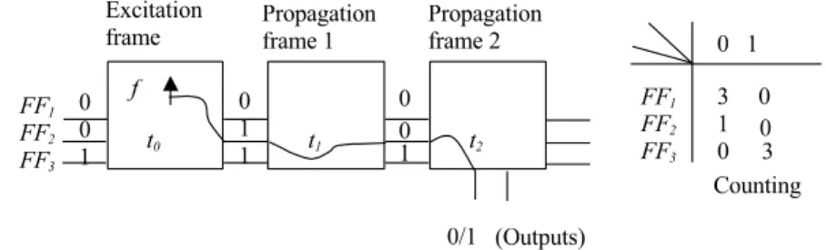
Example 2: In Fig. 4, to excite the fault f, flip-flops FF1, FF2, and FF3 must be set to (001). It takes two time frames to propagate the fault to an output. In the two time frames, FF1, FF2, and FF3 are required to take values of (011) and (001), respectively. From the count-ing of value 1 and 0 in the states set, if f is a hard-to-detect fault, it is natural to select FF1 and FF3 as flip-flops to be reset to 0 and 1, respectively. In addition, as the fault passes through flip-flop FF2 twice, FF2 is better for being scanned.
From the example, it is obvious that we need to record the required states (NS) for excitation and propagation of hard-to-detect faults and also the frequencies (FP) of the flip-flops for the faults to pass through. These data are also good indices for selecting candidate flip-flops for partial scan/reset.
2.3 Structural Relationships Among Flip-Flops
The structural relationships among flip-flops in a circuit play an important role in determining the testability of the circuit. Here a dependence graph [39] is used to describe the structural relationships among flip-flops. Fig. 5 shows the dependence graph for the ISCAS benchmark circuit s400 [38]. In the graph, each node represents a flip-flop or a group of flip-flops, which themselves are in a strongly connected graph, and each branch represents a signal path from a source node to a destination node. In this graph, each node is levelized such that flip-flops in lower levels determine the values of flip-flops in higher levels. The graph provides information about how the signal on one flip-flop may be af-fected by those on some other flip-flops, and about which flip-flops the signal will be able to go through. This information will also be helpful in selecting reset and scan flip-flops.
3. FLIP-FLOP SELECTION FOR SCAN AND RESET
After the above information has been collected, it is then analyzed to help select flip-flops for partial scan or partial reset. The steps are shown in detail in Fig. 6, which shows a sub-process of the process shown in Fig. 2. From the states in the reachable states set RS, we accumulate the occurrence frequencies for 1 and 0 on flip-flop FFn and record them as RS1 (n) and RS0(n), respectively. The smaller the values of RS1(n) or RS0(n) are, the more difficult it will be to set the flip-flop to “1” or “0”, respectively. If RS1(n) is 0 (or very small) and RS0(n) is very large, FFn is a good candidate for being reset to 1 rather than being
Fig. 4. An example showing the excitation and propagation states needed for a hard-to-detect fault. The frequencies of occurrence of 1 and 0 on flip-flops reveal which flip-flops are good/bad candidates for selection for partial scan or reset.
0/1 (Outputs) Propagation frame 2 Propagation frame 1 Excitation frame 0 1 3 0 1 0 0 3 FF1 FF2 FF3 t0 t1 0 0 1 t2 0 0 1 0 1 1 FF1 FF2 FF3 Counting f
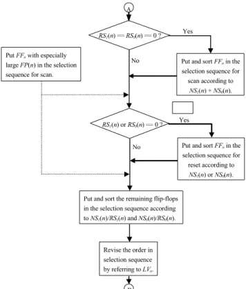
Fig. 6. The sub-process for selecting flip-flops for partial scan/reset. A B Yes No Yes No RS1(n) == RS0(n) == 0 ?
Put and sort FFnin the selection sequence for scan according to
NS1(n) + NS0(n).
RS1(n) or RS0(n) == 0 ?
Put and sort FFnin the selection sequence for reset according to NS1(n) or NS0(n). Put FFnwith especially
large FP(n) in the selection sequence for scan.
Put and sort the remaining flip-flops in the selection sequence according to NS1(n)/RS1(n) and NS0(n)/RS0(n).
Revise the order in selection sequence by referring to LVn.
Fig. 5. The dependence graph of circuit s400.
7 20 21 12 13 14 19 1,2,3,4 5,6,8 9,10,11 17,18 15,16
scanned. If both RS1(n) and RS0(n) are equal to 0 (or very small), then FFn is a good candidate for scanning. When there is more than one flip-flop for which both RS1(n) and RS0(n) are equal to 0, we need more information to help distinguish the importance of these flip-flops in order to improve the level of testability.
As mentioned in section 2.2, we collect the needed states for excitation and propaga-tion of hard-to-detect faults in the states set NS. Let NS1(n) and NS0(n) be the frequency of occurrence of 1 and 0, respectively, on flip-flop FFn in NS. The larger the values of NS1(n) and NS0(n), the more often the values 1 and 0 are required on flip-flop FFn, respectively, during test generation. For those flip-flops for which both RS1(n) and RS0(n) are equal to 0, we add the values of NS1(n) and NS0(n) for each flip-flop and sort these flip-flops according to the summation in descending order. These flip-flops are first selected for partial scan as they are difficult to be set values, i.e., either 1 or 0, but are urgently required for test generation.
Example 3: Assume a circuit with six flip-flops has the data RS1(n), RS0(n), NS1(n), and NS0 (n) as shown in the following:
FFn RSl(n) RS0(n) NSl(n) NS0(n) 1 0 0 17 22 2 16 34 20 42 3 0 0 48 31 4 0 50 29 19 5 50 0 10 42 6 28 22 15 24
Because flip-flops FF1 and FF3 have RS1 and RS0 values both equal to 0, we calculate the summation of NS1 and NS0 for these flip-flops and obtain the values 17 + 22 = 39 and 48 + 31 = 79, respectively. Consequently, we put FF3 first in order and FF1 second for scanning. For the next consideration, the flip-flops for which only SS1(n) or SS0(n) are equal to 0 are put into the selection sequence. They are considered for resetting and sorted in order according to their NS1(n) or NS0(n) values. The larger the NS1(n)( or NS0(n)) is, the more urgent it is for FFn to be reset to 1(or 0).
Example 4: In Example 3, RS1(4) and RS0(5) are equal to 0 but RS0(4) and RS1(5) are not. Therefore, they will be selected for resetting rather than scanning. Because NS1(4) = 29 < NS0(5) = 42, flip-flop FF5, which is to be reset to 0, will be selected before FF4, which is to be reset to 1.
In section 2.2, we explained that besides the required states set NS, we also collect the frequencies of passing through the flip-flops for the hard-to-detect faults during propagation. Let FP(n) be the frequency of faults passing through flip-flop FFn. A flip-flop with a large FP(n) is also a good selection for scanning because it can let many hard-to-detect faults become easily observed. In our experiment, we put the flip-flops whose FP(n) s were at least twice the values of the others next in the selection sequence. It is noteworthy that as scan design requires much more hardware overhead and test application time than reset does, selecting flip-flops with respect to FP(n) is usually considered behind the previ-ous selection for reset. However, the value of NS1(n) or NS0(n) for reset selection may sometimes be very small; i.e., selecting the corresponding flip-flop for reset will not in-crease the circuit's testability very much, so the flip-flops with large FP(n) values will be considered first to achieve better testability.
Example 5: Assume that the circuit in Example 3 has the FP(n) values for the six flip-flops shown in the following table. Obviously, FF3 will be considered for scanning as it has a larger FP value compared to the others.
FFn FP(n) 1 14 2 2 3 57 4 19 5 5 6 11
For the remaining flip-flops, neither RS1(n) nor RS0(n) being equal to 0, which im-plies that they may not be suitable for resetting because the resulting circuit may only increase a few new valid states. More analysis of reachable states and required states is needed to find the possibility of increasing valid states if resetting these flip-flops. For simplicity, in our process, they are chosen for scanning according to the values of NS1(n)/ RS1(n) and NS0(n)/RS0(n), which are accounted for because the flip-flop with larger NS1(n) (or NS0(n)) and smaller RS1(n) (or RS0(n)) is more demanding than those with the inverse condition.
Example 6: For the data given in Example 3, flip-flops FF2 and FF6 have RS1 and RS0 values which are not equal to 0. For flip-flop FF2, NS1(2)/RS1(2) = 20/16 = 1.25 and NS0(2)/ RS0(2) = 42/34 = 1.24. For flip-flop FF6, NS1(6)/RS1(6) = 15/28 = 0.54 and NS0(6)/RS0(6) = 24/22 = 1.09. Having larger values, FF2 will therefore be placed in the selection sequence before FF6. Both flip-flops are for scan only when being chosen to aid the design for testability.
To find the fewest flip-flops for DFT to improve the highest testability, it is theoreti-cal to choose the best flip-flop each time and to then obtain new data for the revised circuit for the next round of analysis. The iterations are continued until the required testability for the circuit is achieved. Analyzing the data is fast, but running test generation takes much time. To quickly obtain an enough testable circuit, we apply a strategy of selecting
indepen-dent flip-flops each time. Here indepenindepen-dent means that these flip-flops do not affect each
other in the dependence graph; i.e., there is no directed path from one flip-flop to another in the dependence graph. For two flops in a directed path in the graph, selecting one flip-flop for scanning may affect the testability of the other one; therefore, they are not suitable for simultaneous selection for DFT purposes. As for independent flip-flops, if they are adjacent in the flip-flop selection sequence, they can be selected at the same time for DFT in order to reduce number of iterations required for test generation.
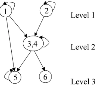
Example 7: Assume a circuit with six flip-flops has the dependence graph shown in Fig. 7. Flip-flops FF1 and FF2 are independent because there are no directed paths between them. If after analyzing the data for scanning and resetting, we find that they are placed in adjacent positions in the selection sequence, then they can be selected together for DFT purposes in the same iteration.
In Fig. 7, the dependence graph has three levels. The values of the flip-flops in the lower level implicitly determine those of the flip-flops in higher levels. Consequently, the flip-flops in the lower level are likely to be selected first for resetting or scanning because they may affect the testability of the flip-flops in higher levels. Let LVn be the level of FFn in the dependence graph. For the flip-flops with higher LVn’s, they affect less number of flip-flops if being reset and behave more likely to be only new primary outputs if being scanned. Accordingly, when two flip-flops are adjacent in the selection sequence and have comparable values for resetting or scanning, their levels in the dependence graph are used to slightly modify the selection order.
Example 8: In Fig. 7, assume that we obtain a selection sequence in which flip-flops FF6 and FF3 have similar values and FF6 is prior to FF3. Their positions will be exchanged according to the consideration for levels in the dependence graph.
Example 9: We will use circuit s400 [38], whose dependence graph is shown in Fig. 5, to explain the entire process of selecting flip-flops. After performing test generation, we found that none of the RS1(n) and RS0(n) values of the flip-flops were equal to 0 based on the reachable states of test patterns. There was also no flip-flop with an especially large FP (n) value. Therefore, we compared the flip-flops with NS1(n)/RS1(n) and NS0(n)/RS0(n). From the comparison, we found that flip-flop FF12 had the largest values and, hence, was a good selection for scanning. The scanned circuit was then subjected to test generation again. None of the new RS1(n) and RS0(n) of all the flip-flops were equal to 0, either. There was still no flip-flop with an especially large FP(n). According to the NS1(n)/RS1(n) and NS0 (n)/RS0(n) of the remaining flip-flops, we found the next flip-flop, i.e., FF8, for being se-lected for scan. The process can be continued until the required fault coverage is achieved. It will be shown in the next section that, for circuit s400, we only selected two flip-flops for scanning but obtained fault coverage comparable to that of the other two scanning methods, which required three and five flip-flops, respectively. The fault efficiency, i.e., the sum of the counts of detectable and identified untestable faults divided by the total number of faults for this circuit appears to be 100% for the test generation of all the methods. This means that the reported levels of fault coverage are the highest achievable results for the three selection methods. Therefore, our method requires fewer scan flip-flops but achieves the same level of testability as do the other methods for circuit s400.
Fig. 7. A dependence graph of a circuit with six flip-flops.
1 2 3,4 5 6 Level 1 Level 2 Level 3
4. EXPERIMENTAL RESULTS
The above procedure, called RESCAN, was implemented, on a PC with a Pentium II 300Mhz CPU and 256M RAM. A BACK[40,41]-like test generator was implemented and used for test generation in the procedure. Table 1 shows the results obtained using RESCAN compared to those of three other recently reported methods for partial scan [14, 31, 32]. In Table 1. Comparison of RESCAN with the other three methods of scan selection. In the table, ‘-’ means no data given, and ‘*’ means that the original circuits are at least different in terms of the number of flip-flops.
BELLONA[31] Opscan[32] IDROPS[14] RESCAN
Circuit #FF #SFF FC(%) #SFF FC(%) #SFF FC(%) #SFF #RFF FC(%) #Iter. s298 14 1 94.8 1 94.8 – – 1 0 98.05 1 s344 15 1 96.2 3 98.8 – – 1 0 98.54 1 s349 15 2 98.0 3 98.3 – – 1 0 98.00 1 s382 21 3 97.2 5 97.5 – – 3 0 97.49 3 s386 6 – – 2 92.2 – – 2 0 94.79 2 s400 21 3 95.8 5 95.8 – – 2 0 95.75 2 s420 16 – – – – 3 20.9 0 3 50.23 3 s444 21 2 94.5 5 94.9 3 93.2 2 0 93.25 1 3 0 94.73 2 s526 21 2 91.4 7 98.7 3 87.2 2 0 93.69 2 s526n 21 – – 8 99.1 – – 6 0 99.10 3 s641 19 1 95.7 5 94.2 – – 0 1 99.36 1 s713 19 1 87.4 5 88.1 – – 0 1 92.97 1 s820 5 1 98.9 2 100.0 – – 1 0 100.00 1 0 1 99.53 1 s832 5 1 97.7 2 98.4 – – 1 0 98.39 1 s953 29 – – 3 100.0 – – 3 0 100.00 2 s1423 74 34 97.6 – – 15 95.8 26 2 95.27 7 s1488 6 1 99.1 2 100.0 – – 1 0 99.87 1 s1494 6 1 98.3 3 99.2 – – 1 0 99.00 1 s5378 179 27 93.8 80 97.5 21 94.7 15 8 94.91 10 s9234 228 – – – – *27 *79.9 41 13 73.74 9 s13207 669 – – – – *78 *76.5 82 4 77.15 7 s15850 597 – – – – *66 *65.2 69 7 65.58 4 s35932 1728 – – 150 89.8 – – 0 8 89.72 1
the table, column #FF lists the number of flip-flops in each circuit, and column #SFF gives those selected for scan. Column #RFF lists the number of flip-flops selected for reset design. Column FC(%) shows the final fault coverage of the circuits. For RESCAN, col-umn #Iter gives the number of iterations required to select flip-flops. As shown in the table, BELLONA[31] and Opscan[32] provided most of the circuits except s5378 with 100%
fault efficiency. In other words, the fault coverage of most of the circuits listed in the table
is the highest achievable using the two methods. However, our method can achieve even higher fault coverage for many circuits by selecting fewer flip-flops for DFT. The authors of IDROPS[14] used a simulation-based test generator[42] which could not identify untestable faults, so that they could not achieve the highest fault coverage for the circuits. The authors also did not provide results for many circuits. In addition, they did not explain why the number of flip-flops for circuits s9234, s13207, and s15850 was 211, 638, and 534, respectively, which results are different from those provided by ISCAS89[38]. From the table, RESCAN exhibits better results with fewer scanned flip-flops but higher fault cover-age for most of the circuits compared to the other methods. For some circuits, RESCAN can even use flip-flops for resetting only yet can achieve higher fault coverage than the other three methods using scanning. Some circuits, e.g. s420 listed, in the table can be further run to achieve 100% fault efficiency or coverage. For the larger circuits, iterations of test generation take much time, which is the common disadvantage of flip-flop selection methods that use test generation results. Due to the limitations of our test generator, the real fault coverage for each of the large circuits can be even higher than shown. As the run time for the other methods is not available for comparison, we only show the time required by our test generator in Table 2 for some of the circuits. For the circuits that are not shown in the table, their test generation jobs were usually interrupted for various reasons, which prevented us from conducting complete runs and recording the time used. We estimated that our test generator took more than two weeks to run iterations for each circuit. If available, more efficient test generators may be used to speed up collection of needed data. Another suggested way is to first find test patterns for the easily testable faults only. The remaining faults may all be considered as difficult to detect, and their required states for fault excitation and propagation can then be quickly found by means of a simplified test generation process. The test generator need not take time to ensure whether there are test patterns or not. The process of collecting data for analysis can then be speeded up, but the obtained data may not be accurate enough for selecting the correct flip-flops.
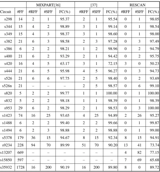
Table 3 lists the results obtained using RESCAN compared with those of two other methods that incorporated both partial reset and partial scan [36, 37]. The two methods both applied reset selection first and then scan selection for flip-flops, which is different from our mixed selection approach. They need some criteria to decide how many reset flip-flops are sufficient. In our approach, we choose the best flip-flop(s) for scanning or reset-ting according to whether they can make most of the hard-to-detect faults testable. The information about the reachable states, the states required for fault excitation and propagation, the number of hard-to-detect faults passing through each flip-flop, and the structural depen-dence graph enable our approach to select flip-flops more accurately. As for MIXPART [36], in addition to partial scan and reset, it employs a partial observation technique that makes some selected flip-flops obserable. However, RESCAN out-performs it significantly on many circuits. Comparing to [37], RESCAN still exhibits better results for many circuits. As for circuits larger than s5378, because our test generator cannot achieve 100% fault efficiency, we believe that the real fault coverage can be even higher if better test generator is used.
5. CONCLUSIONS
In this work, a novel methodology for flip-flop selection for partial resetting and partial scanning on sequential circuits designed to improve testability has been proposed. Previous methods which combined scanning and resetting selected flip-flops first for reset-ting and then for scanning. The proposed method is not limited to this selection approach but instead finds the flip-flops that most improve the testability improvement if selected for scanning or resetting. To find the best flip-flops, the procedure collects information about the reachable states of test patterns and states required for hard-to-detect faults through test generation and simulation, and explores for structural inter-connection information of flip-flops. The obtained data are analyzed to produce a selection sequence for all the flip-flops being reset or scanned. With respect to the highest priority flip-flop(s), the process revises the circuit with scan or reset and subjects the resulting circuit to test generation again. This can be repeated until the required fault coverage is achieved. Experimental results on ISCAS benchmark circuits show that the methodology requires fewer flip-flops for scanning and resetting to achieve a higher level of testability than can be achieved by the other scan only and mixed scan/reset methods. This proves the better accuracy achieved by our method in selecting flip-flops. In order to reduce the time needed, superior test generators are needed to speed up the process of searching for test patterns and states required for selecting flip-flops.
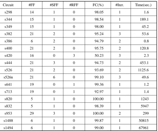
Table 2. Run time of RESCAN on some benchmark circuits.
Circuit #FF #SFF #RFF FC(%) #Iter. Time(sec.)
s298 14 1 0 98.05 1 1.6 s344 15 1 0 98.54 1 189.1 s349 15 1 0 98.00 1 45.2 s382 21 2 0 95.24 3 53.6 s386 6 2 0 94.79 2 0.8 s400 21 2 0 95.75 2 120.8 s420 16 0 3 50.23 3 2.3 s444 21 3 0 94.73 2 453.1 s526 21 2 0 93.69 2 1125.6 s526n 21 6 0 99.10 3 49.6 s641 19 0 1 99.36 1 1.2 s713 19 0 1 92.97 1 1.4 s820 5 1 0 100.00 1 1243 s832 5 1 0 98.39 1 5947 s953 29 3 0 100.00 2 299 s1488 6 1 0 99.87 1 50815 s1494 6 1 0 99.00 1 67961
REFERENCES
1. T. Grason and A. W. Nagle, “Digital test generation and design for testability,”
Jour-nal of Digital Systems, Vol. 5, No. 4, 1981, pp. 319-359.
2. T. W. Williams and K. P. Parker, “Design for testability - a survey,” in Proceedings of
IEEE, Vol. 71, No. 1, 1983, pp. 98-112.
3. E. B. Eichelberger and T. W. Williams, “A logic design structure for LSI testability,” in
Proceedings of 14th Design Automation Conference, 1977, pp. 462-468.
4. W. Trischler, “Incomplete scan path with an automatic test generation methodology,” in Proceedings of International Test Conference, 1980, pp. 153-162.
5. T. H. Chen and M. A. Breuer, “Automatic design for testability via testability measures,”
IEEE Transactions on Computer-Aided Design of Integrated Circuits and Systems,
Vol. CAD-4, 1985, pp. 3-11.
Table 3. Comparison of RESCAN with two other methods that combine reset and scan.
MIXPART[36] [37] RESCAN Circuit #FF #RFF #SFF FC(%) #RFF #SFF FC(%) #RFF #SFF FC(%) s298 14 2 1 95.37 2 1 95.54 0 1 98.05 s344 15 4 2 98.89 3 1 99.14 0 1 98.54 s349 15 4 3 98.37 3 1 98.60 0 1 98.00 s382 21 6 3 98.58 2 3 97.28 0 3 97.49 s386 6 2 2 98.21 1 2 98.96 0 2 94.79 s400 21 6 2 93.29 2 1 94.42 0 2 95.75 s420 16 4 5 63.17 3 1 72.15 3 0 50.23 s444 21 6 5 95.98 4 5 96.27 0 3 94.73 s526 21 6 6 97.75 2 5 98.40 0 2 93.69 s526n 21 – – – 2 5 98.57 0 6 99.10 s820 5 2 2 99.77 1 1 100.00 0 1 100.00 s832 5 2 2 98.18 1 1 98.39 0 1 98.39 s953 29 6 2 98.29 2 1 98.53 0 3 100.00 s1423 74 16 25 93.65 4 25 94.89 2 26 95.27 s1488 6 2 2 99.40 2 2 99.66 0 1 99.87 s1494 6 2 3 98.88 2 2 98.88 0 1 99.00 s5378 179 36 15 94.67 8 15 92.34 8 15 94.91 s9234 228 94 70 89.99 51 70 90.20 13 41 73.74 s13207 669 – – – – – – 4 82 77.15 s15850 597 – – – – – – 7 69 65.68 s35932 1728 16 200 90.19 16 200 89.80 8 0 89.72
6. K. S. Kim and C. R. Kime, “Partial scan by use of empirical testability,” in
Proceed-ings of International Conference on Computer-Aided Design, 1990, pp. 314-317.
7. V. Chickermane and J. H. Patel, “An optimization based approach to the partial scan design problem,” in Proceedings of International Test Conference, 1990, pp. 377-386. 8. H. Gundlach, B. Koch, and K.-D. Muller-Glaser, “On the selection of a partial scan path with respect to target faults,” in Proceedings of European Design Automation
Conference, 1991, pp. 219-223.
9. M. Abromovici, J. J. Kulikowski, and R. K. Roy, “The best flip-flops to scan,” in
Pro-ceedings of International Test Conference, 1991, pp. 166-173.
10. V. Chickermane and J. H. Patel, “A fault oriented partial scan design approach,” in
Proceedings of International Conference on Computer-Aided Design, 1991, pp.
400-403.
11. P. S. Parikh and M. Abromovici, “A cost-based approach to partial scan,” in
Proceed-ings of 30th Design Automation Conference, 1993, pp. 255-259.
12. P. S. Parikh and M. Abromovici, “Testability-based partial scan analysis,” Journal of
Electronic Testing: Theory and Applications, Vol. 7, 1995, pp. 61-70.
13. D. Xiang, S. Venkataraman, W. K. Fuchs, and J. H. Patel, “Partial scan design based on circuit state information,” in Proceedings of 33rd Design Automation Conference, 1996, pp. 807-812.
14. M. S. Hsiao, G. S. Saund, E. M. Rudnick, and J. H. Patel, “Partial scan selection based on dynamic reachability and observability information,” in Proceedings of
Interna-tional Conference on VLSI Design, 1998, pp. 174-180.
15. R. Gupta, R. Gupta, and M. A. Breuer, “BALLAST: A methodology for partial scan design,” in Proceedings of International Symposium on Fault-Tolerant Computing, 1989, pp. 118-125.
16. K.-T. Cheng and V. D. Agrawal, “An economical scan design for sequential logic test generation,” in Proceedings of International Symposium on Fault-Tolerant Computing, 1989, pp. 28-35.
17. A. Kunzmann and H.-J. Wunderlich, “An analytical approach to the partial scan problem,”
Journal of Electronic Testing: Theory and Applications, 1990, pp. 163-174.
18. K.-T. Cheng and V. D. Agrawal, “A partial scan method for sequential circuits with feedback,” IEEE Transactions on Computers, Vol. 39, No. 4, 1990, pp. 544-548. 19. D. H. Lee and S. M. Reddy, “On determining scan flip-flops in partial-scan design,” in
Proceedings of International Conference on Computer-Aided Design, 1990, pp.
322-325.
20. S. Bhawmik, C. J. Lin, K.-T. Cheng, and V. D. Agrawal, “PASCANT: A partial scan and test generation system,” in Proceedings of Custom Integrated Circuit Conference, 1991, pp. 17.3.1-17.3.4.
21. S. Park and S. B. Akers, “A graph theoretic approach to partial scan design by K-cycle elimination,” in Proceedings of International Test Conference, 1992, pp. 303-311. 22. H. B. Min and W. A. Rogers, “A test methodology for finite state machines using partial
scan design,” Journal of Electronic Testing: Theory and Applications, Vol. 3, 1992, pp. 127-137.
23. S. E. Tai and D. Bhattacharya, “A three stage parital scan design method using the sequential circuit flow graph,” in Proceedings of International Conference on VLSI
Design, 1994, pp. 101-106.
select-ing partial scan flip-flops,” in Proceedselect-ings of 31st Design Automation Conference, 1994, pp. 81-86.
25. P. Ashar and S. Malik, “Implicit computation of minimum-cost feedback-vertex sets for partial scan and other applications,” in Proceedings of 31st Design Automation
Conference, 1994, pp. 77-80.
26. T. Ono, “Selecting partial scan flip flops for circuit partitioning,” in Proceedings of
International Conference on Computer-Aided Design, 1994, pp. 646-650.
27. A. Balakrishnan and S. T. Chakradhar, “Peripheral partitioning and tree decomposition for partial scan,” in Proceedings of International Conference on VLSI Design, 1998, pp. 181-186.
28. V. D. Agrawal, K.-T. Cheng, D. D. Johnson, and T. Lin, “A complete solution to the partial scan approach,” in Proceedings of International Test Conference, 1987, pp. 44-51.
29. V. D. Agrawal, K.-T. Cheng, and D. D. Johnson, “Designing circuits with partial scan,”
IEEE Design and Test of Computers, 1988, pp. 8-15.
30. H. K. T. Ma, S. Devadas, A. R. Newton, and A. Sangiovanni-Vincentelli, “An incom-plete scan design approach to test generation for sequential machines,” in Proceedings
of International Test Conference, 1988, pp. 730-734.
31. I. Park, D. S. Ha, and G. Sim, “A new method for partial scan design based on propaga-tion and justificapropaga-tion requirements of faults,” in Proceedings of Internapropaga-tional Test
Conference, 1995, pp. 413-422.
32. D. Xiang and J. H. Patel, “A global algorithm for the partial scan design problem Using Circuit State Information,” in Proceedings of International Test Conference, 1996. 33. I. Pomeranz and S. M. Reddy, “On the role of hardware reset in synchronous sequential
circuit test generation,” IEEE Transactions on Computers, 1994, pp. 1100-1105. 34. B. Mathew and D. G. Saab, “Partial reset: an inexpensive design for testability approach,”
in Proceedings of European Design Automation Conference, 1993, pp. 151-155. 35. M. Abramovici, P. S. Parikh, B. Mathew, and D. G. Saab, “On selecting flip-flops for
partial reset,” in Proceedings of International Test Conference, 1993, pp. 1008-1012. 36. P. S. Parikh and M. Abramovici, “On combining design for testability techniques,” in
Proceedings of International Test Conference, 1995, pp. 423-429.
37. H. C. Liang, C. L. Lee, and J. E Chen, “Partial reset and scan for flip-flops based on states requirement for test generation,” in Proceedings of the 16th IEEE VLSI Test
Symposium, 1998, pp. 341-346.
38. F. Brglez, D. Bryan, and K. Kozminski, “Combinational profiles of sequential bench-mark circuits,” in Proceedings of International Symposium on Circuits and Systems, 1989, pp. 1929-1934.
39. H.-C. Liang, C. L. Lee, and J. E. Chen, “Identifying invalid states for sequential circuit test generation,” IEEE Transactions on Computer-Aided Design of Integrated Circuits
and Systems, Vol. 16, No. 9, 1997, pp. 1025-1033.
40. W.-T. Cheng, “The BACK algorithm for sequential test generation,” in Proceedings of
International Conference on Computer Design, 1988, pp. 66-69.
41. W.-T. Cheng and S. Davidson, “Sequential circuit test generator(STG) benchmark results,” in Proceedings of International Symposium on Circuits and Systems, 1989, pp. 1939-1941.
42. P. Prinetto, M. Rebaudengo, and M. Sonza Reorda, “An automatic test pattern genera-tor for large sequential circuits based on genetic algorithms,” in Proceedings of
Hsing-Chung Liang ( ) received the B.S., M.S., and Ph.D. degrees in electronics engineering from National Chiao Tung University, Taiwan, R.O.C., in 1989, 1991, and 1997, respectively. From 1997 to 1999, he was an Assistant Professor in the Depart-ment of Electronic Engineering, Van Nung Institute of Technology. Since August 1999, he joined the faculty of the Department of Elec-tronic Engineering, Chang Gung University. His research interests include VLSI testing and design for testability.
Chung Len Lee ( ) obtained his B.S. from National Taiwan University in 1968 and M.S. and Ph.D. from Carnegie Mellon University in 1971 and 1975 respectively, all in Electrical Engineering. He has been with Department of Electronics Engineering, National Chiao Tung University, since 1975, engag-ing in teachengag-ing and research in the fields of semiconductor devices, integrated circuits, VLSI, computer aided design and testing. He has supervised over 120 M.S. and Ph.D. students to complete their thesis and has published over 250 papers in the above areas. He has been involved in various technical activities in the above areas in Taiwan as well as in Asia. He is on the editorial board of JETTA.