Fabrication of NiSi 2 nanocrystals embedded in SiO 2 with memory effect by oxidation
of the amorphous Si Ni SiO 2 structure
P. H. Yeh, H. H. Wu, C. H. Yu, L. J. Chen, P. T. Liu, C. H. Hsu, and T. C. Chang
Citation: Journal of Vacuum Science & Technology A 23, 851 (2005); doi: 10.1116/1.1913678
View online: http://dx.doi.org/10.1116/1.1913678
View Table of Contents: http://scitation.aip.org/content/avs/journal/jvsta/23/4?ver=pdfcov Published by the AVS: Science & Technology of Materials, Interfaces, and Processing
Articles you may be interested in
Structural and magnetic stability of Fe 2 NiSi
AIP Conf. Proc. 1591, 1501 (2014); 10.1063/1.4873010
Low-power memory device with NiSi 2 nanocrystals embedded in silicon dioxide layer Appl. Phys. Lett. 87, 193504 (2005); 10.1063/1.2126150
Mechanisms of arsenic segregation to the Ni 2 Si SiO 2 interface during Ni 2 Si formation Appl. Phys. Lett. 87, 181910 (2005); 10.1063/1.2125124
Direct evidence of internal Schottky barriers at NiSi 2 precipitates in silicon by electron holography J. Appl. Phys. 97, 063707 (2005); 10.1063/1.1863432
Electrical transport properties of NiSi 2 layers synthesized by metal vapor vacuum-arc ion implantation: Temperature dependence and two-band model
Fabrication of NiSi
2nanocrystals embedded in SiO
2with memory effect
by oxidation of the amorphous Si/ Ni/ SiO
2structure
P. H. Yeh
Department of Materials Science and Engineering, National Tsing Hua University, Hsin-Chu, Taiwan, Republic of China
H. H. Wu
Institute of Electronics of Electro-Optical Engineering, National Chiao Tung University, Hsin-Chu, Taiwan, Republic of China
C. H. Yu
Department of Materials Science and Engineering, National Tsing Hua University, Hsin-Chu, Taiwan, Republic of China
L. J. Chena兲
Department of Materials Science and Engineering, National Tsing Hua University, Hsin-Chu, Taiwan, Republic of China
P. T. Liu
Institute of Electronics of Electro-Optical Engineering, National Chiao Tung University, Hsin-Chu, Taiwan, Republic of China
C. H. Hsu
National Synchrotron Radiation Research Center, Hsin-Chu, Taiwan 300, Republic of China
T. C. Chang
Department of Physics and Institute of Electro-Optical Engineering, National Sun Yat-sen University, Kaohsiung, Taiwan, Republic of China and National Nano Device Laboratories, 1001-1 Ta-Hsueh Road, Hsin-Chu 300 Taiwan, Republic of China
共Received 15 November 2004; accepted 14 March 2005; published 27 June 2005兲
NiSi2nanocrystals embedded in the SiO2layer exhibiting a memory effect have been formed by dry
oxidation of an amorphous Si/ Ni/ SiO2 structure at 900 °C. A pronounced capacitance-voltage
hysteresis was observed with a memory window of 1 V under the 2 V programming voltage for the samples. For dry oxidation at 800 °C, no distinct memory effect was detected. The processing of the structure is compatible with the current manufacturing technology of the semiconductor industry. The structure represents a viable candidate for low-power nanoscaled nonvolatile memory devices. © 2005 American Vacuum Society. 关DOI: 10.1116/1.1913678兴
I. INTRODUCTION
Recently, a memory-cell structure employing a semicon-ductor or metal nanocrystals as storage elements in metal-oxide-semiconductor 共MOS兲 field transistors has received much attention as a promising candidate to replace a conven-tional dynamic random array memory or flash memories for future high-speed and low-power consumer memory devices.1–5Most studies have focused on the fabrication on Si and Ge nanocrystals in a MOS structure.6–14The use of a floating gate composed of distributed nanocrystals reduces the problems of charge loss encountered in conventional floating-gate electrical erasable programmable read-only memory devices. It allows thinner tunnel oxide and, thereby, smaller operating voltages, better endurance and retention, and faster program/erase speed.7–9 The self-assembling of silicon or germanium nanocrystals embedded in SiO2 layers
has been widely investigated, and strong memory effects in MOS devices were reported.6–14 The metal nanocrystals’ memory has exhibited several advantages, such as stronger
coupling with the conduction channel, a wide range of avail-able work functions, higher density of states around the Fermi level, and smaller energy perturbation due to carrier confinement.2 The metal nanocrystals were usually fabri-cated by thermal annealing of the ultrathin metal film on the tunnel oxide.2,3In the present study, NiSi2nanocrystals
em-bedded in SiO2exhibiting memory effect were fabricated by
oxidation of amorphous Si/ Ni/ SiO2structure.
II. EXPERIMENTAL PROCEDURES
Six-inch 共100兲 oriented p-type silicon wafers were cleaned with standard RCA process, followed by a dry oxi-dation in an atmospheric pressure chemical vapor deposition furnace to form a 3 nm thick tunnel oxide. Subsequently, a 3.5 nm thick nickel layer was deposited onto the tunnel oxide by electron-beam evaporation. The nickel layer was capped by a 12.5 nm thick amorphous Si layer deposited also by sputtering. A schematic diagram of the structure is shown in Fig. 1共a兲. The stacked structure was, afterwards, dry oxidized for 10 min at 800 or 900 °C to form a layer with control oxide on the top. NiO or NiSi2 nanocrystals were found to a兲Electronic mail: [email protected]
precipitate and embed between tunnel oxide and control ox-ide, as depicted in Fig. 1共b兲. Finally, Al gate electrode was patterned and sintered, as illustrated in Fig. 1共c兲. The struc-tural examinations were carried out in a transmission elec-tron microscope 共TEM兲 and synchrotron radiation facility using the x-ray absorption near-edge structure 共XANES兲 analysis technique.15 The capacitance-voltage 共C-V兲 mea-surements were performed by a precision LCR meter 共HP 4284A兲 to study the electron charging and discharging ef-fects of the NiSi2nanocrystals.
III. RESULTS AND DISCUSSION
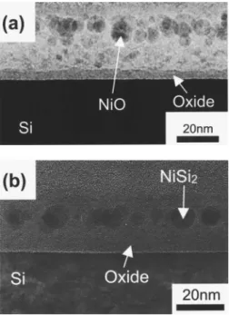
Figure 2 shows typical bright-field, cross-sectional TEM images. In Fig. 2共a兲, a sample after 800 °C dry oxidation is shown. The nanocrystals were found to distribute in the con-trol oxide randomly. However, for samples dry oxidized at 900 °C, as seen in Fig. 2共b兲, well-separated and spherical NiSi2nanocrystals embedded in the SiO2layer are observed.
The top a-Si layer was completely oxidized to serve as the control oxide. Figure 3共a兲 shows the plan-view TEM image of a 900 °C oxidized sample. The mean size and aerial den-sity of the NiSi2nanocrystals were measured to be about 8.5
nm and 2.5⫻1011/ cm2, respectively. The size distribution of
the nanocrystals is shown in Fig. 3共b兲. The nanocrystals were located between the tunnel oxide and the control oxide, with-out diffusing into the oxide. The characteristic is beneficial for the reliability and the yield of the memory device. The variation in morphology of these two samples with different oxidation temperatures is related to the rate of silicide for-mation. As the a-Si film was oxidized, oxygen may diffuse to the oxide/ Si interface to form silicon oxide. If the NiSi2
nanocrystals were already formed, they may move farther away from the oxide/ Si interface. As a result, the selection of oxidation temperature and time are critical for forming nanocrystals. In growing SiO2 film from Si, a film of SiO2 with a thickness of x0 consumes a layer of crystalline Si 共c-Si兲 about 0.45x0. Therefore, a Si substrate about 3.2 nm
thick was oxidized to contribute to about a 7 nm thick SiO2 in addition to the 3 nm thick tunnel oxide.
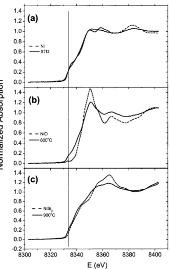
X-ray absorption near-edge structure analysis was used to determine the oxidation states of the samples.15–18 In XANES, a core electron is excited to higher bound or qua-sibound states, which contain information about coordination geometry and electronic aspects of the absorbing atom. Among most of the XANES studies, the standard materials with known valence are utilized as references, and compared with the unknown samples. Therefore, the measurements are frequently qualitatively analyzed, not quantitatively. The ab-sorption edge of metallic Ni 共at 8 333 eV兲 is marked in the figure by a vertical line to guide the eye. In the present study,
FIG. 1. Stacked structures of a-Si/ Ni/ SiO2/ Si共a兲 before and 共b兲 after dry
oxidation.共b兲 Well-separated and spherical nanocrystals are embedded in the SiO2layer, and共c兲 the structure for capacitance-voltage measurement.
FIG. 2. Cross-sectional TEM micrographs for samples after dry oxidation at 共a兲 800 °C and 共b兲 900 °C. In 共a兲 The NiO nanocrystals are distributed in the control oxide randomly and in 共b兲 well-separated and spherical NiSi2
nanocrystals embedded in the SiO2layer are seen.
852 Yeh et al.: Fabrication of NiSi2nanocrystals 852
the Ni foil, NiO powder, and the epitaxial NiSi2layer on Si
substrate were used as reference samples. As shown in Fig. 4共a兲, the edge position reflects zero-valence metal character of the as-deposited Ni layer. However, the local atomic struc-ture seems to be quite disordered共like amorphous materials兲 so that the spectral features appear much less resolved as compared with those of Ni foils. For samples dry oxidized at 800 °C, substantial oxidation occurred, giving rise to many spectral features similar to what NiO exhibits, as shown in Fig. 4共b兲. This is attributed to the diffusion of nickel atoms into the a-Si film first, followed by oxidation. For the samples annealed at 900 °C, the features in its XANES spec-trum look similar to those of NiSi2, as shown in Fig. 4共c兲. It
is thought that the formation of NiSi2 and oxidation of a-Si
film occurred first and the diffusion of Ni atoms was im-peded.
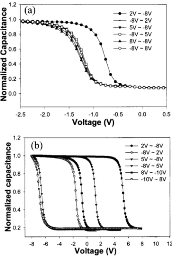
Figure 5 shows the forward and reverse sweep C-V char-acteristics, indicating the electron charging and discharging effects of the nanocrystals embedded in SiO2. The
bidirec-tional C-V sweeps were performed from deep inversion to deep accumulation and in reverse, which exhibited an
elec-tron charging effect. As seen in Fig. 5共a兲, the C-V character-istic of the samples dry oxidized at 800 °C is rather poor. The hysteresis is clockwise, which is due to gate injection. It is correlated to the inactive NiO nanocrystals inside the control oxide, as seen in Fig. 2共a兲. The electron and the hole injec-tions into the NiO nanocrystals are easier from the gate than from the Si substrate. If the oxidation temperature and time are well controlled, the memory effect can be improved. As shown in Fig. 5共b兲, for samples oxidized at 900 °C with the voltage swept from 2 to共−8兲 V and back to 2 V, an outstand-ing threshold voltage shift of 1 V is observed. As the whisked voltages were increased to 5 and 8 V, more obvious
C-V shifts of 8 and 13 V respectively, are seen. It is
per-ceived that the hysteresis is counterclockwise, which is due to injection of electrons from the deep inversion layer and injection of holes from the deep accumulation layer of Si substrate.19 The result of the C-V shift indicates that the charging effects of NiSi2 nanocrystals are more significant
than those of the semiconductor nanocrystals. In Fig. 6, the threshold voltage shift opens with increasing the gate voltage for the samples oxidized at 900 °C. For the samples oxidized at 800 °C, the significant memory window is lacking. The TEM images and the C-V characteristics indicate that the
FIG. 3.共a兲 Plan-view TEM image of a sample after 900 °C dry oxidation and 共b兲 the size distribution of the nanocrystals.
FIG. 4. XANES spectra for 共a兲 as-deposited Ni layer and Ni foil, 共b兲 a sample oxidized at 800 °C and NiO powders, and共c兲 a sample oxidized at 900 °C and epitaxial NiSi2on silicon.
nickel diffusion can be alleviated by increasing the process temperature. The memory effect of the samples with a pro-cess temperature of 1000 °C was found to be rather poor, possibly due to the agglomeration of NiSi2at a temperature
above the eutectic temperature共993 °C兲 for Ni-Si system.
Figure 7共a兲 shows the band diagrams with different gate polarities of the memory device for the samples oxidized at 800 °C. With the NiO nanocrystals randomly distributed in the control oxide, the energy well is near the gate electrode. When the gate polarity is negative, the electrons directly tun-nel from the electrode and become trapped in the NiO nano-crystals. On the other hand, the electrons will tunnel back to the electrode. From the TEM image shown in Fig. 2共a兲, the control oxide became inactive with distribution of the NiO nanocrystals throughout the oxide. The electrons may tunnel back to the electrode even though the gate polarity is not positive. The memory effect of the samples is therefore not distinct. For the samples dry oxidized at 900 °C, as illus-trated in Fig. 7共b兲, when the device is written or pro-grammed, the electrons tunnel directly from the Si substrate through the tunnel oxide, and are trapped in the NiSi2
nano-crystals. On the other hand, when the device is erased, the electrons may tunnel back to the deep accumulation layer of Si substrate. The control oxide is utilized to prevent the car-riers of gate electrode from injecting into the NiSi2
nanocrystals by Fowler-Nordheim tunneling.
The most important advantage using the metal nanocrys-tals over their semiconductor counterparts is that the metal nanocrystals do not bear a voltage drop from gate voltage,
FIG. 5.共a兲 C-V hysteresis loops of 共a兲 NiO nanocrystals in samples oxidized at 800 °C and共b兲 NiSi2nanocrystals in samples oxidized at 900 °C.
FIG. 6. Plots showing that the windows of Vtopen with increasing gate
voltage for samples oxidized at 900 °C. On the other hand, for samples oxidized at 800 °C, no significant memory windows are evident.
FIG. 7. 共a兲 Band diagrams with different gate polarities of the memory device for the samples oxidized at共a兲 800 °C and 共b兲 900 °C with “write” and “erase” operations.
854 Yeh et al.: Fabrication of NiSi2nanocrystals 854
which means all the voltages provided from control gate are dropped to tunnel oxide and control oxide. The operating voltage of the memory devices with conventional floating gate or semiconductor nanocrystals embedded in SiO2 is
above 7 or 5 V. In our approach to fabricate the NiSi2
nano-crystals embedded in SiO2 by dry oxidation 900 °C, a lower
programming voltage of 2 V realizes a significant threshold voltage shift of 1 V. The voltage is sufficient to be defined as “1” and “0” by a typical sensing amplifier for a memory device.
To find the retention characteristics of the structure, an accelerated test was conducted at 150 °C. The retention data are incorporated into Fig. 8 for a retention time up to 10 h. Although the drifts of C-V curves are evident, possibly due to the presence of the fixed charges at the oxide/Si interface, the nonvolatility of the data共i.e., a shift of more than 1 V in threshold voltage兲 is maintained throughout.
IV. CONCLUSIONS
NiSi2 nanocrystals embedded in SiO2 have been
fabri-cated with appropriate control of the process temperature and time. In samples dry oxidized at 900 °C, the mean size and aerial density of NiSi2nanocrystals were measured to be 8.5
nm and 2.5⫻1011/ cm2, respectively. A significant C-V
hys-teresis of voltage shift of 1 V was observed. The advantages
of the method are that it is simple and well controlled. The implementation of the present structure is compatible with the current manufacturing technology of semiconductor in-dustry and represents a viable candidate for low-power nanoscaled nonvolatile memory devices.
ACKNOWLEDGMENTS
This work was performed at National Nano Device Labo-ratory and was supported by National Nano Device Labora-tory under Contract No. 92A0500001 and the National Sci-ence Council under Contract No. NSC92-2215-E-110-006.
1S. Tiwari, F. Rana, K. Chan, H. Hanafi, C. Wei, and D. Buchanan, Tech.
Dig. - Int. Electron Devices Meet. 1995, 521.
2Z. Liu, C. Lee, V. Narayanan, G. Pei, and E. C. Kan, IEEE Trans.
Elec-tron Devices 49, 1606共2002兲.
3Z. Liu, C. Lee, V. Narayanan, G. Pei, and E. C. Kan, IEEE Trans.
Elec-tron Devices 49, 1614共2002兲.
4S. Tiwari, F. Rana, H. Hanafi, A. Hartstein, E. F. Crabbe, and K. Chan,
Appl. Phys. Lett. 68, 1377共1996兲.
5H. I. Hanafi, S. Tiwari, and I. Khan, IEEE Trans. Electron Devices 43,
1553共1996兲.
6S. Tiwari, F. Rana, K. Chan, L. Shi, and H. Hanafi, Appl. Phys. Lett. 69,
1232共1996兲.
7J. J. Welser, S. Tiwari, S. Rishton, K. Y. Lee, and Y. Lee, IEEE Electron
Device Lett. 18, 278共1997兲.
8J. D. Blauwe, IEEE Trans. Nanotechnol. 1, 72共2002兲.
9A. Kanjilal, J. L. Hansen, P. Gaiduk, A. N. Larsen, N. Cherkashin, A.
Claverie, P. Normand, E. Kapelanakis, D. Skarlatos, and D. Tsoukalas, Appl. Phys. Lett. 82, 1212共2003兲.
10L. W. Teo, W. K. Choi, W. K. Chim, V. Ho, C. M. Moey, M. S. Tay, C. L.
Heng, Y. Lei, D. A. Antoniadis, and E. A. Fitzgerald, Appl. Phys. Lett.
81, 3639共2002兲.
11V. Craciun, I. W. Boyd, A. H. Reader, and E. W. Vandenhoudt, Appl.
Phys. Lett. 65, 3233共1994兲.
12Y. C. King, T. J. King, and C. Hu, Tech. Dig. - Int. Electron Devices
Meet. 1998, 115.
13K. Das, M. NandaGoswami, R. Mahapatra, G. S. Kar, H. N. Acharya, S.
Maikap, J. H. Lee, and S. K. Ray, Appl. Phys. Lett. 84, 1386共2004兲.
14T. C. Chang, S. T. Yan, C. H. Hsu, M. T. Tang, J. F. Lee, Y. H. Tai, P. T.
Liu, and S. M. Sze, Appl. Phys. Lett. 84, 2581共2004兲.
15F. W. Lytle, R. B. Greegor, D. R. Sandstrom, E. C. Marques, J. Wong, C.
L. Spiro, G. P. Huffman, and F. E. Huggins, Nucl. Instrum. Methods 226, 542共1984兲.
16P. Zhang and T. K. Sham, Appl. Phys. Lett. 81, 736共2002兲.
17S. Y. Ha, J. Park, T. Ohta, G. Kwag, and S. Kim, Electrochem. Solid-State
Lett. 2, 461共1999兲.
18G. Dalba, P. Fornasini, R. Grisenti, F. Rocca, and I. Chambouleyron,
Appl. Phys. Lett. 81, 625共2002兲.
19D. N. Kouvatsos, V. L. Sougleridis, and A. G. Nassiopoulou, Appl. Phys.
Lett. 82, 397共2003兲. FIG. 8. Variations of the C-V hysteresis loops for samples heated at 150 °C
for up to 10 h.