Light-emitting polymer space-charge-limited transistor
Chun-Yu Chen, Yu-Chiang Chao, Hsin-Fei Meng, and Sheng-Fu Horng
Citation: Applied Physics Letters 93, 223301 (2008); doi: 10.1063/1.3027057
View online: http://dx.doi.org/10.1063/1.3027057
View Table of Contents: http://scitation.aip.org/content/aip/journal/apl/93/22?ver=pdfcov Published by the AIP Publishing
Articles you may be interested in
Polymer space-charge-limited transistor as a solid-state vacuum tube triode Appl. Phys. Lett. 97, 223307 (2010); 10.1063/1.3513334
Low voltage active pressure sensor based on polymer space-charge-limited transistor Appl. Phys. Lett. 95, 253306 (2009); 10.1063/1.3266847
Polymer space-charge-limited transistor
Appl. Phys. Lett. 88, 223510 (2006); 10.1063/1.2207838
Effective ionic charge polarization using typical supporting electrolyte and charge injection phenomena in molecularly doped polymer light-emitting diodes
J. Appl. Phys. 92, 5971 (2002); 10.1063/1.1513886
Electrode versus space-charge-limited conduction in organic light-emitting diodes Appl. Phys. Lett. 75, 2035 (1999); 10.1063/1.124907
This article is copyrighted as indicated in the article. Reuse of AIP content is subject to the terms at: http://scitation.aip.org/termsconditions. Downloaded to IP: 140.113.38.11 On: Wed, 30 Apr 2014 22:48:42
Light-emitting polymer space-charge-limited transistor
Chun-Yu Chen,1Yu-Chiang Chao,1Hsin-Fei Meng,1,a兲and Sheng-Fu Horng21Institute of Physics, National Chiao Tung University, Hsinchu 300, Taiwan 2
Department of Electrical Engineering, National Tsing Hua University, Hsinchu 300, Taiwan
共Received 19 June 2008; accepted 25 October 2008; published online 1 December 2008兲
Polymer light-emitting transistor is realized by vertically stacking a top-emitting polymer light-emitting diode on a polymer space-charge-limited transistor. The transistor modulates the current flow of the light-emitting diode by the metal-grid base voltage. The active semiconductor of the transistor is poly共3-hexylthiophene兲. Yellow poly共para-phenylene vinylene兲 derivative is used as the yellow emitting material. As the cathode is fixed at −12 V and the grid base voltage varies from 0.9 to −0.9 V the light emission is turned on and off with on luminance up to 1208 cd/m2. The
current efficiency of the light-emitting transistor is 10 cd/A. © 2008 American Institute of Physics. 关DOI:10.1063/1.3027057兴
Semiconductor devices based on conjugated polymers have been widely explored for polymer light-emitting diode 共PLED兲, field-effect transistor 共FET兲, and solar cell. One of the promising applications of the polymer devices is the thin, flexible, and lightweight active-matrix display.1 Unlike liquid-crystal display, which is voltage-controlled, in poly-mer display a PLED in each pixel is controlled by a driving transistor, which supplies the current. The current output of the transistor must be very stable and uniform. Currently polycrystalline silicon FET suffers from a uniformity prob-lem, while amorphous silicon and organic FET have rather low carrier mobility and long-term stability problems.2 In addition, FET is a horizontal device while PLED is a vertical device, so they can only be placed side by side and the ap-erture ratio of the pixel is limited by the size of the FET. One possible way to replace the conventional combination of LED driven by FET is the organic light-emitting transistor, which combines the electrical switching and the light gen-eration capabilities in a single device.3 However, so far the applications of light-emitting transistor is hindered because the emission efficiency is rather low, and the emission zone is in a narrow line pattern, which is unfavorable for display applications. In this work, a non-FET polymer light-emitting transistor is demonstrated by vertically integrating a top-emitting PLED on a polymer vertical metal-base transistor. The vertical transistor is used to modulate the current and therefore the luminance of the PLED. Uniform luminance over 1000 cd/m2 is achieved. The current efficiency of the light-emitting transistor is 10 cd/A at yellow emission. The aperture ratio is basically 100% because the light emitted upward is not shielded by the vertical metal-base transistor underneath with roughly the same area. Light generation in vertical transistor was reported before,4,5 but these early works show poor luminance no more than 1 cd/m2. The
high luminance is achieved by a vertical polymer light-emitting transistor, the space-charge-limited transistor 共SCLT兲. This transistor has a high output current density around 27 mA/cm2, which can drive PLED to high
lumi-nance.
Organic vertical metal-base transistors with various architectures and operation principles have been
developed6–16 to overcome the limits of conventional hori-zontal organic FETs. The channel length of vertical metal-base transistor is defined by the thickness of the organic layer, and the output current is modulated by a base electrode embedded in the organic semiconductor. Two types of verti-cal metal-base transistors, namely the hot-carrier transistor13,14 and SCLT,15,16 show promising performance. In this work the polymer SCLT is vertically integrated with a PLED. The carriers are injected from the emitter into the semiconductor, passing through the openings on the metal grid base, and finally arriving at the collector. The potential distribution and current flow between emitter and collector is controlled by the voltages of grid. Because the emitter-collector distance is only tens of nanometers, high current output and high speed can be achieved even for low carrier mobility typical for PLED, thus solving the problems of or-ganic FETs for current output and speed. The fabrication is even simpler than FET as no photolithography is needed. In addition the high current output and potentially high speed SCLT shows far better stability than the organic FET. Due to the current channel confinement, organic FET characteristics are easily affected by the chemical and physical defects at the gate dielectric-semiconductor interface. SCLT is free from the unpredictable conditions at the dielectric interface because its current is uniformly distributed in the bulklike organic light-emitting diodes.
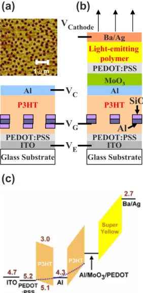
The device structure of the polymer SCLT with a silicon monoxide insulating layer on the aluminum grid is shown in Fig. 1共a兲. A 400 Å layer of poly共3,4-ethylenedioxythiophene兲 doped with polystyrene sulfonated acid 共PEDOT:PSS兲 is spin-coated onto the indium tin oxide 共ITO兲 glass substrate to flatten the ITO surface and serve as the emitter for holes. A layer of 200 Å poly共3-hexylthiophene兲 共P3HT兲 is then spin coated from chloroben-zene solution 共1.5 wt %兲. After annealing at 200 °C for 10 min, a spin rinsing with xylene is used to remove the remain-ing soluble part of P3HT. The substrate is submerged into 2000 Å共1000 Å兲 polystyrene spheres ethanol solution with 0.24 wt % 共0.4 wt %兲 for 40 s and then transferred into a beaker with boiling isopropanol solution for 10 s. The sub-strate is immediately blown dry in a unidirectional nitrogen flow to form two dimensional colloidal arrays without aggre-gation. After 150 Å Al grid is evaporated as grid; the sample is annealed in high vacuum共10−6 torr兲. 500 Å SiO is
evapo-a兲Author to whom correspondence should be addressed. Electronic mail:
APPLIED PHYSICS LETTERS 93, 223301共2008兲
0003-6951/2008/93共22兲/223301/3/$23.00 93, 223301-1 © 2008 American Institute of Physics
This article is copyrighted as indicated in the article. Reuse of AIP content is subject to the terms at: http://scitation.aip.org/termsconditions. Downloaded to IP: 140.113.38.11 On: Wed, 30 Apr 2014 22:48:42
rated to prevent large leakage current from grid to collector. After the polystyrene spheres are removed by an adhesive tape, another layer of 800 Å P3HT is spin coated from xy-lene solution共3 wt %兲. A 400 Å Al collector is finally de-posited to complete the polymer SCLT with active area of 3 mm2. The atomic force microscope 共AFM兲 image of Al grid with 2000 Å opening diameter is also shown in Fig. 1共a兲, which is taken after removing the polystyrene spheres. The opening density is about 7 openings/m2. For the
light-emitting transistor as shown in Figs. 1共b兲 and1共c兲, the fab-rication procedure of the vertical transistor is the same as described above, while the procedures of the PLED are de-scribed below. A 30 Å MoO3 anode is deposited on the Al collector with same shadow mask, followed by spin coating 450 Å PEDOT:PSS from an aqueous solution diluted by iso-propanol in equal volume. The diluted PEDOT:PSS solution contains also 2 wt % surfactant 共Zonyl FSN兲 to facilitate aqueous PEDOT:PSS solution to be spinned on a substrate coated with hydrophobic polymer. Poly共para-phenylene vi-nylene兲 polymer derivative 共Super Yellow by Merck兲 is spin coated from toluene as light-emitting layer of 100 nm. The semitransparent cathode Ba共100 Å兲/Ag共150 Å兲 is then de-posited to complete the device with an active area of 4 mm2.
Due to convenience in mask alignment the LED area is
slightly larger than the transistor area of 3 mm2. The
PEDOT:PSS layer prevents the transistor from being dis-solved by the solution of the light-emitting polymer.
The polymer SCLT is in a diode sandwich structure with a third metal base electrode inserted into the semiconductor to control the vertical carrier flow between the emitter and the collector. In this work, additional high vacuum annealing after Al grid deposition is used for increasing the P3HT mo-bility and current density of ITO/PEDOT:PSS/P3HT/Al di-ode. The transistor output current can be enhanced from 1 mA/cm2 to as high as 27 mA/cm2. The improved
poly-mer SCLT with grid opening diameters of 2000 Å is shown in Fig. 2共a兲. JCand VCare the collector current density and the collector voltage, respectively. The ITO electrode is com-monly grounded and the Al collector is negatively biased at
VC. Various grid voltages are applied to Al grid base to modulate the current. The negative collector current density
JCmeans the holes flow from the transistor and are collected by the Al collector. An insulating SiO layer is deposited on Al grid to reduce the grid leakage current from Al grid to collector. Such SiO layer allows a higher collector bias and higher output current before grid diode breaks down. When
VCis −7 V and VGis −0.9 V, the transistor output current density is about 27 mA/cm2and the on/off ratio is 386. The
maximum on/off ratio is 428 when VCis reduced to −6 V.
JG as a function of VC is also shown in Fig.2共b兲. The re-maining JGmay come from the leakage path in the nondense SiO layer and the Al sidewall close to the opening. As the transistor is on, the current gain JC/JGof this transistor is around 104. Besides, the annealing procedure is expected to have two results. First, annealing in high vacuum causes oxygen dedoping of P3HT. Second, annealing helps the poly-mer chains to reorganize to have a high mobility and high current density. The collector current density of 27 mA/cm2 is about the same as PLED under normal operation. The Light-emitting polymer Ba/Ag PEDOT:PSS MoO3 Al Glass Substrate ITO P3HT Al PEDOT:PSS
(a)
(b)
Glass Substrate ITO P3HT PEDOT:PSSV
EV
GV
CV
Cathode(c)
1μmSiO
Al
FIG. 1. 共Color online兲 共a兲 Device structure of the polymer SCLT and the
AFM image of Al grid with 2000 Å opening diameter.共b兲 Device structure
of the top-emitting polymer light-emitting transistor.共c兲 Energy profile of
the top-emitting polymer light-emitting transistor.
0 5 10 15 20 25 30 -JC (mA/cm 2 )
V
G(V) -0.9 -0.3 0.3 0.9 1.5 2.1 2.7(a)
(b)
0 2 4 6 8 -10 -5 0 5 10 -JG (uA/cm 2 ) -VC(V)FIG. 2.共Color online兲 The electric characteristics of the polymer SCLT with
2000 Å openings on Al grid.共a兲 Collector current density JCand共b兲 grid
current density JGas a function of collector voltage VCat various grid biases
VG.
223301-2 Chen et al. Appl. Phys. Lett. 93, 223301共2008兲
This article is copyrighted as indicated in the article. Reuse of AIP content is subject to the terms at: http://scitation.aip.org/termsconditions. Downloaded to IP: 140.113.38.11 On: Wed, 30 Apr 2014 22:48:42
transistor is therefore able to drive a PLED vertically stacked with roughly the same area.
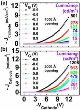
The characteristics of the top-emitting Super Yellow PLED with the structure ITO/PEDOT:PSS/Super Yellow/ Ba/Ag is given in Fig.3. The current efficiency is 10.6 cd/A. In the light-emitting transistor the PLED is fabricated on top of the Al collector of SCLT with a MoO3 layer in between. The electrical characteristics of the polymer light-emitting transistor with opening diameters of 1000 and 2000 Å on Al grid are shown in Figs. 4共a兲 and 4共b兲, respectively. This structure is effectively a PLED connected in series to a vari-able resistor, which modulates the PLED current and there-fore luminance. The ITO emitter electrode is commonly grounded and various VGis applied to the Al grid base. The voltage applied to the semitransparent cathode Vcathodeis
var-ied from 0 to −12 V.
Voltage VCof the Al collector in the SCLT component is floating and determined by the voltage drop across the PLED. It spontaneously matches the currents of the SCLT component and the PLED component. The luminance at various VG for Vcathode at −12 V is shown in Fig. 4. The
maximum luminance around 500 and 1200 cd/m2 is achieved for polymer light-emitting transistor with grid opening diameters of 1000 and 2000 Å, respectively. The minimum luminance can be turned off by increasing VGuntil large leakage current occurs. This device not only fulfills the minimum luminance requirement for the display panel, but also achieves by far the highest luminance among various light-emitting transistor principles. The on-off contrast of the luminance is yet to be improved. The residual off-luminance cannot be switched off by the grid voltage before grid diode breakdown. A stronger insulation of the grid is needed to withstand a more positive grid voltage.
The structure and operation principle of the polymer light-emitting transistor above is different from previous re-port on static induction transistor,5where the light is emitted inside the channel of the vertical transistor. In our device the light emission and driving are separated into different com-ponents of the device with a floating electrode between them. The performance of each component is therefore not com-promised by the integration with the other component. The composite electrode Al/MoO3/PEDOT:PSS layer has two
advantages. First, the electrons injected from the cathode will not reach P3HT. The efficiency and color of the light emission are therefore not ruined by the unwanted recombi-nation in P3HT. Second, the electrons injected from the cath-ode will not arrive at the Al grid and cause a large JG and poor current gain.
In summary, the performance of the polymer SCLT is enhanced by annealing and by insulator on grid metal to have high output current density and high current gain. The top-emitting polymer light-emitting transistor based on the SCLT is demonstrated. This transistor has low voltage, high light-emission aperture ratio, and high luminance good enough for display applications.
This work is supported by the National Science Council of Taiwan under Contract No. NSC96-2112-M-009-036. The authors thank Merck, Inc. for providing the Super Yellow polymer.
1T. K. Chuang, M. Troccoli, P. C. Kuo, A. Jamshidi-Roudbari, M. K.
Hatalis, I. Biaggio, and A. T. Voutsas, Appl. Phys. Lett. 90, 151114
共2007兲.
2M. L. Chabinyc, F. Endicott, B. D. Vogt, D. M. DeLongchamp, E. K. Lin,
Y. Wu, P. Liu, and B. S. Ong,Appl. Phys. Lett. 88, 113514共2006兲.
3F. Cicoira and C. Santato,Adv. Funct. Mater. 17, 3421共2007兲.
4Z. Xu, S. H. Li, L. Ma, G. Li, and Y. Yang,Appl. Phys. Lett. 91, 092911
共2007兲.
5K. Kudo, Curr. Appl. Phys. 5, 337共2005兲.
6Y. Yang and A. J. Heeger,Nature共London兲 372, 344共1994兲.
7S. Fujimoto, K. Nakayama, and M. Yokoyama, Appl. Phys. Lett. 87,
133503共2005兲.
8K. Kudo, D. X. Wang, M. Iizuka, S. Kuniyoshi, and K. Tanaka,Synth.
Met. 111, 11共2000兲.
9Y. Watanabe and K. Kudo,Appl. Phys. Lett. 87, 223505共2005兲.
10K. Fujimoto, T. Hiroi, K. Kudo, and M. Nakamura, Adv. Mater. 19, 525
共2007兲.
11M. Yi, S. Yu, C. Feng, T. Zhang, D. Ma, M. S. Meruvia, and I. A.
Hummelgen,Org. Electron. 8, 311共2007兲.
12S. S. Cheng, C. Y. Yang, Y. C. Chuang, C. W. Ou, M. C. Wu, S. Y. Lin,
and Y. J. Chan,Appl. Phys. Lett. 90, 153509共2007兲.
13Y. C. Chao, S. L. Yang, H. F. Meng, and S. F. Horng,Appl. Phys. Lett.87,
253508共2005兲.
14Y. C. Chao, M. H. Xie, M. Z. Dai, H. F. Meng, S. F. Horng, and C. S. Hsu,
Appl. Phys. Lett. 92, 093310共2008兲.
15Y. C. Chao, H. F. Meng, and S. F. Horng,Appl. Phys. Lett. 88, 223510
共2006兲.
16Y. C. Chao, H. F. Meng, S. F. Horng, and C. S. Hsu,Org. Electron.9, 310
共2008兲.
FIG. 4. 共Color online兲 The electric characteristics of the polymer
light-emitting transistor with共a兲 1000 Å and 共b兲 2000 Å openings on Al grid.
The luminances at VCathode= −12 V are also demonstrated for various VG
condition.
0
4
8
12
16
0
3
6
9
12
10
210
310
410
5 Luminan ce (C d /m 2 ) Efficien cy (Cd/A) V (V) 800 600 W avelength (nm ) 400FIG. 3. 共Color online兲 The efficiency and luminance of the top-emitting
PLED.
223301-3 Chen et al. Appl. Phys. Lett. 93, 223301共2008兲
This article is copyrighted as indicated in the article. Reuse of AIP content is subject to the terms at: http://scitation.aip.org/termsconditions. Downloaded to IP: 140.113.38.11 On: Wed, 30 Apr 2014 22:48:42