國
立
交
通
大
學
機械工程學系
碩士論文
以微控制器 HD64F2612FA20 實現三相直流無刷馬達控制
Realization for Brushless DC Motor Control
by Micro Controller HD64F2612FA20 chip
研 究 生:陳晉輝
指導教授:成維華 教授
以微控制器 HD64F2612FA20 實現三相直流無刷馬達控制
Realization for Brushless DC Motor Control
by Micro Controller HD64F2612FA20 chip
研 究 生:陳晉輝 Student: Jin-Huei Chen 指導教授:成維華 Advisor: Wei-Hua Chieng
國立交通大學 機械工程學系
碩士論文 A thesis
Submitted to Department of Mechanical Engineering
College of Engineering National Chiao Tung University
in partial Fulfillment of the Requirements for the Degree of
Master In
Mechanical Engineering
July 2010
Hsinchu, Taiwan, Republic of China
i
以微控制器 HD64F2612FA20 實現三相直流無刷馬達控制
研 究 生:陳晉輝 指導教授:成維華 博士 國立交通大學機械工程學系摘要
直流無刷馬達因為具有高效率、高轉速以及高扭力等優點。不同的控制 方式會使直流無刷馬達有不同的效能,若欲增進直流無刷馬達的控制效 率,則需使用更複雜的控制策略。本文將使用瑞蕯出產之 HD64F2612FA20 的 16 位元微控制器,其多達 15 相的 PWM 輸出且具備板上編程(on-board programming)能力,利於程式的撰寫與發展,並以此晶片實現三相直流無 刷馬達控制。其中使用霍爾感測器訊號估算轉速並透過外部控制面板顯示 轉速,透過比例積分控制器實現轉速閉迴路控制。本文發展 16 位元之高效 能晶片完成直流無刷馬達控制,以利未來更複雜之控制策略的實現。 關鍵字:微控制器、直流無刷馬達、六步方波、脈衝寬度調變ii
Realization for Brushless DC Motor Control
by Micro Controller HD64F2612FA20 chip
Student: Jin-Huei Chen Advisor: Dr. Wei-Hua Chieng
Department of Mechanical Engineering
National Chiao Tung University
Abstract
The BLDC motors are everywhere because of its advantages such as high
efficiency, high speed and high torque. Different control method can cause different efficiency, if someone wants to improve the efficiency of BLDC motor,
the more complex control strategy needs to be used. This paper will use the microcontroller HD64F2612FA20 which is produced by Renesas company
because that it has at most 15-phase PWM output and the On-board programming function, these are helpful for programming and the development
of program. In this paper, the 16-bit and high efficiency’s microcontroller of brushless DC motor control will be implemented. The hall sensor’s signal is
used to estimate motor’s speed which is displayed through digital operator. The speed closed-loop control is realized by Proportional-Integral controller. This
paper will use 16-bit and high efficiency microcontroller to implement brushless DC motor control for more complex control strategy in the future.
Keywords: Microcontroller (MCU), BLDC motor, Six-step square waveform, PWM
iii
誌 謝
感謝成維華教授與鄭時龍博士,在這兩年來的教導與付出,每當遇 到瓶頸時都會給予適當的方向與提示,讓我在學校中學到做研究的態度 與方法。感謝育能學長、俊旭學長、志方老師在口試時的提醒與建議。 感謝實驗室向斌學長、嘉豐學長、秉霖學長對實驗室的付出,感謝實驗 室的同學們,一起分擔學習上的壓力,感謝實驗室學弟們的幫忙與協 助,讓我無後顧之憂地專心完成學業。 感謝我的家人,在這兩年的時間資助我取得碩士學歷。感謝我的室 友們,因為有你們,讓我在新竹唸書時不孤單。 最後感謝我的女朋友,這兩年因為有妳,所以我不寂寞,一路陪著 我完成這人生重要的一段,新竹台北的距離考驗,我們克服了。iv
Content
摘要 ... i Abstract ... ii 誌 謝 ... iii Content ... iv List of Tables ... viList of Figures ... vii
Chapter 1 Introduction ... 1
1.1 Motive and Objectives ... 1
1.2 Thesis Organization ... 1
Chapter 2 Basic Theories and Knowledge ... 3
2.1 The Feature of Brushless DC Motors ... 3
2.1.1 Structure of Brushless DC Motors ... 4
2.1.2 Hall Sensor ... 4
2.2 Commutation Method ... 5
2.3 The Mathematical Model of BLDC Motors ... 6
2.4 Speed Control Analysis ... 8
Chapter 3 Software Setup ... 11
3.1 Main program ... 11
3.2 Initialization ... 11
3.2.1 Serial communication interface (SCI) ... 11
3.2.2 Timer pulse unit (TPU) ... 12
3.2.3 A/D Converter ... 14
v 3.3 Interrupt routine ... 15 3.3.1 RXI interrupt ... 15 3.3.2 TGIA0 interrupt ... 15 3.3.3 TCIV1 interrupt ... 15 3.3.4 TCIV2 interrupt ... 16 3.4 Speed estimation ... 16 3.5 PI controller ... 17
Chapter 4 Hardware Setup ... 18
4.1 The structure of system ... 18
4.2 Introduction of MCU ... 18 4.3 MCU circuit ... 19 4.4 Digital operator ... 20 4.5 BLDC motor’s specification ... 21 Chapter 5 Experiment ... 22 5.1 Hardware setup ... 22 5.2 Experiment result ... 23 Chapter 6 Conclusion ... 25 Reference ... 27
vi
List of Tables
Table 2.1 120 degree six-step square commutation table ... 28
Table 3.1 PWM output registers and output pins ... 29
Table 4.1 Two Mode correspond to their pins state respectively ... 29
Table 4.2 Digital operator’s protocol ... 30
Table 4.2 Digital operator’s protocol (continue) ... 31
Table 4.3 Digital operator’s data format ... 31
Table 4.4 The specification of BLDC motor ... 32
Table 5.1 Specification of tachometer ... 33
Table 5.2 Specification of Adlee driver ... 33
Table 6.1 Internal priority of MCU ... 34
vii
List of Figures
Fig 2.1 The structure of BLDC motors ... 36
Fig 2.2 The Hall effect ... 36
Fig 2.3 Schematic of the inverter and motor ... 37
Fig 2.4 Six-step sequences waveforms ... 37
Fig 2.5 The procedure of the commutation ... 38
Fig 2.5 The procedure of the commutation (continue) ... 39
Fig 2.6 The equivalent model of a BLDC motor ... 40
Fig 2.7 A BLDC motor equal circuit ... 40
Fig 3.1 Main program flowchart ... 41
Fig 3.2 TGIA0 interrupt flowchart ... 42
Fig 3.3 Hall signal ... 43
Fig 3.4 Close-loop control block diagram ... 43
Fig 4.1 The structure of system ... 43
Fig 4.2 The HD64F2612F340 chip’s pin arrangement ... 44
Fig 4.3 The layout of MCU circuit ... 44
Fig 4.4 MAX232CPE ... 45
Fig 4.5 BLDC motor ... 45
Fig 5.1 Inverter ... 46
Fig 5.2 Hardware setup ... 46
Fig 5.3 Six-step waveform ... 47
Fig 5.4 Hall signal’s waveform ... 48
Fig 5.5 Speed error ... 48
viii
Fig 5.6 Speed response without load at 1000 rpm ... 49 Fig 5.7 Speed response without load at 3000 rpm ... 50
1
Chapter 1 Introduction
1.1 Motive and Objectives
Motor is around in our life, such as scanner, hardware, printer DVD players,
compressors, etc. In order to improve the efficiency of motor control, we need some control strategy, for this purpose, the micro controller unit is applied, such
as Application Specific Integrated Circuit (ASIC). The 8-bit micro controller unit is used popularly and extensively because of its low-cost, simplicity, and
easy to development firmware. As the development of the micro controller unit, the efficiency of the micro controller unit is more powerful and variety of
capabilities. For higher control efficiency, the more complex control strategy will be applied. The 8-bit micro controller unit will become inadequate for
motor control, so to development of the 16-bit micro controller unit used to motor control is needed.
In this thesis, we will realize the brushless DC motor control by micro controller unit HD64F2612FA20 chip, which is published by the Renesas
company.
1.2 Thesis Organization
At first, the motive and objective is presented in chapter 1. In chapter 2, we
2
difference between outrunner and inrunner of the BLDC’s structure, and explaining the Hall sensor’s theory and application, commutation method’s
procedure. After that, the mathematical model of BLDC motor is induced. Finally, the speed control is concerned.
In chapter 3, the program flowchart will show that the process of program, including MCU’s peripheral functions and interrupts. The method of speed
estimation will be discussed and a PI controller will be applied.
In chapter 4, this chapter indicates the structure of system and the
specification of MCU, digital operator and BLDC motor.
The experiment result is in chapter 5, and chapter 6 is my conclusion, some
3
Chapter 2 Basic Theories and Knowledge
A brushless DC (BLDC) motor is a machine that convert power from
electric energy to mechanical energy, its stator is a class three-phase stator like that of an induction motor and the rotor has surface-mounted permanent magnet.
In section 2.1, we introduce the feature of BLDC motors. That is why we choose BLDC motors. Then the mathematical modeling of BLDC motors will be
included in section 2.2. The BLDC motors need an inverter and a position sensor to replace the brushes and commutator, so the commutation can be
executed, and the procedure will be illustrated in section 2.3. In section 2.4, the speed control analysis is performed.
2.1 The Feature of Brushless DC Motors
A BLDC motor is composed of a permanent magnet synchronous motor that transfers electrical power to mechanical energy. It uses the transistors’ on and
off states to control the commutation according to the hall sensor. BLDC motors have many advantages, such as higher reliability, low electrical noise and low
maintenance, long-life, and easy to control, etc. They have high power density, and lower inertia allowing for faster dynamic response to reference commands
compared to induction motor. Unfortunately, the cost of BLDC’s driver is higher, so the application companies are not willing to take the place of the
conventional motor drives due to their higher cost. Thus, it is needed to lower the cost by use of micro controller unit.
4
2.1.1 Structure of Brushless DC Motors
Fig2.1 shows the basic structure of BLDC motors, there are permanent magnets on the rotor and the armature is on the stator. In all BLDC motors, the
stator-coils are stationary, BLDC motors have several physical configurations, typically separate to Outrunner or Inrunner. Outrunners have high torque at low
PRMs and more poles which usually set up in triplets to keep the three groups of windings, Inrunners can spin fast and have better response to commands but
have weak torque. They all rotate by magnetic force and change of magnetic field.
2.1.2 Hall Sensor
When a BLDC motor rotates around, we need to know the motor’s position.
In order to do this, the Hall sensor is applied. The Hall sensor replaces the traditional commutator and brushes because of its higher efficiency and low
maintenance. The Hall sensor uses the Hall effect to output variable voltage in response to changes in magnetic field. As shown in Fig 2.2, a voltage called the
Hall voltage, , is applied to the rectangular metal, and the rectangular metal is placed in a perpendicular magnetic field, . According to the Lorentz force, the
electrons and holes in the metal are apart to different side, and accumulate on the surface of the metal. This leaves equal and opposite charges exposed on the
5
force so that the other following electrons and holes will not be affected. This phenomenon is called the Hall effect.
B d I K dne IB VH =− = (2-1)
2.2 Commutation Method
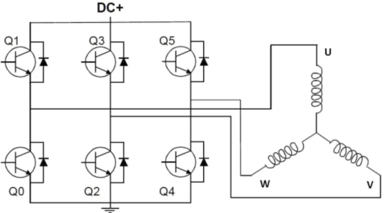
In order to control BLDC motors, it also needs an inverter, Fig2.3 shows its
schematic. The inverter consists of six transistors, controls the current which flows to motor so that we can change the outer stator’s magnetic field according
to the Hall sensor’s signal, and then generates torque.
The six-step sequences is the typically and the must general commutation
method for a BLDC motor, the six inverter’s transistors switch according to the six-step sequences and Hall sensor’s signal to produce the phase current
waveforms, as shown in Fig 2.4. For simplicity, we assume that the currents are in rectangular shapes, and the stator’s inductance voltage may be neglected.
Thus, Table 2.1 indicates the sequence of the conducting phase, we call that “ six-step square commutation table”.
At the step 1, Q5、Q0 transistors switch on, so the current can flow Q5 →
W → → Q0, at step 2, Q3、Q0 transistors switch on, so the current can flow
Q3 → V → → Q0. At the switching moment, because that motor is
inductive load, the current which passes the winding can’t shut down as the switch is right off. Instead, the current will decrease gradually. For decreasing
6
the current of inductance (∆IL) gradually in the motor, we need a circuit to let
the current flow. So there is a free-wheeling diode accompanied a transistor.
This can ease ∆IL so that we can avoid the peak inductance’s voltage (VL)
induced from rapid change of ∆IL, the inductance’s voltage can be expressed as
t I L V L L ∆ ∆ = (2-2)
Following the table’s sequences, shown in table 2.1, the BLDC motor’s
rotor will rotate around, according to the poles of the rotor, there is a relationship between the electrical angle and mechanical angle, that is
2 _ _
_angle Mechanical angle Pole number
Ellectric = ×
Fig 2.5 shows an example of a BLDC motor with 2 poles of rotor, so when it travels an electrical angle cycles, the inner rotor rotates one revolution, and the
higher of poles number, the higher resolution of the motor’s rotation.
2.3 The Mathematical Model of BLDC Motors
In general, a BLDC motor has a permanent-magnet rotor and its stator
windings are wound to generate the back electromotive force (Back-EMF). The dynamic equations of BLDC motors with Y-connected stator winding are shown
7
Using Kirchhoff’s law and Newton’s law, we can get 3-phase BLDC electromagnetic equation and dynamic equation, which express as follows:
Electromagnetic equation: + − − − − − − + = c b a c b a p p p c b a c b a e e e i i i dt d L M M M L M M M L i i i R R R V V V 0 0 0 0 0 0 (2-3)
The back electromotive force (Back-EMF) express as
+ − = ) 3 2 sin( ) 3 2 sin( ) sin( 2 π θ π θ θ ω e e e e r c b a P K e e e (2-4) Dynamic equation: ) cos( ) ( 2 3 ) sin( ) 2 2 ( θe c b θ c b a t e i i i i i K T = − − + − r L m r T p B p J + + = 2 ω ω (2-5) c b a V V
V , , : a, b, and c phase voltages
c b a i i
i , , : a, b, and c phase currents
c b a e e
e , , : a, b, and c phase back electromotive force
p
8
M : mutual inductance between any two phase
R : stator resistance
r
ω : rotor speed
e
θ : angle between stator phase A and rotor
e
K : Back-EMF constant
p: number of pole pairs
e T : electric torque t K : torque constant L T : load torque J : moment of inertia m B : damping constant
2.4 Speed Control Analysis
The BLDC motor’s equivalent circuit is shown in Fig 2.7. the voltage equation can be derived from the circuits as follows:
E IR V PWM Vs( )= CE(sat) + a + a sat CE s R E V PWM V I = ( )− ( ) − (2-6)
9
) (PWM
Vs : Average effective voltage
) ( sat
CE
V : BJT’s conduct voltages between collection and emitter
I : Equal total current
a
R : Equal total resistance
E : Back-EMF
The conduct voltage term VCE can be neglected because that it is too small, and
the equations become:
E IR PWM Vs( )= a + a s R E PWM V I = ( )− (2-7)
Beside the voltage equation, the torque equation and back-EMF equation are
also needed in order to analyze speed control. The torque equation and back-EMF equation are represented individually as follows:
I K T = t⋅ (2-8) r e K E= ⋅ω (2-9)
Summarizing the equations of (2-7), (2-8), and (2-9), we can analyze situations when BLDC motors are in acceleration or deceleration. In the case of
acceleration, PWM increases results in the average effective voltage increases, according to equation (2-7), the current I also increases, according equation
10
(2-8), the induced torque of stator Tinduced increases follows the current I
increases. When the Tinduced is larger than the loading torque, the motor’s speed
increases. According to the equation (2-9), the back-EMF increases when the motor’s speed increases. The result makes the current I decreases. When the
current I is down, the Tinduced decreases until Tinduced equals to Tload. Therefore,
the speed is not only accelerated but also stable. In the other case of deceleration, the analysis is opposite, PWM decreases results in the average effective voltage
decreases, according to equation (2-7), the current I also decreases, according
equation (2-8), the induced torque of stator Tinduced decreases follow the current I
decreases. When the Tinduced is smaller than the loading torque Tload , the
back-EMF decreases when the motor’s speed decreases. The result makes the
current I increase. When the current I is up , the Tinduced increases until Tinduced
11
Chapter 3 Software Setup
3.1 Main program
The flowchart of main program is shown in Fig 3.1. First, we do the initialization, which enables and initializes SCI (serial communication interface),
TPU (timer pulse unit) and ADC (A/D converter). Setting I/O pin of MCU is also included. Second, we communicate with digital operator for check sequence
and initialize the information that we want to show in LCD. After that, we catch the ASCII code of Menu key to enter the Menu selection mode.
3.2 Initialization
3.2.1 Serial communication interface (SCI)
In SCI initialization, we use the asynchronous mode and following protocol:
SCI2:
Baud Rate: 9600 Data Bit: 8
Stop Bit: 1 Parity Bit: none
12
SCI1:
Baud Rate: 9600
Data Bit: 8 Stop Bit: 1
Parity Bit: none
There are two SCI channels we used, SCI2 is used for PC and SCI1 is used for digital operator. We set TE and RE bits in SCR to open SCI and let RIE bit
enable so that we can allow SCI interrupt.
3.2.2 Timer pulse unit (TPU)
We use TPU0 as our timer for checking hall signal’s status in period,
according to our BLDC motor’s specification, the rated speed is 3000 rpm, the time in every step at rating speed is
) / ( 83 . 0 ) / ( 24 ) ( 60 3000 1 step ms s step rps ≅ ×
By setting TGRA_0, the period is decided, we let the period be 0.1ms. It is enough to avoid missing hall signal’s step.
TPU1 is used for open-loop or close-loop control’s feedback time, and TPU2 is chosen for calculating BLDC motor’s speed,
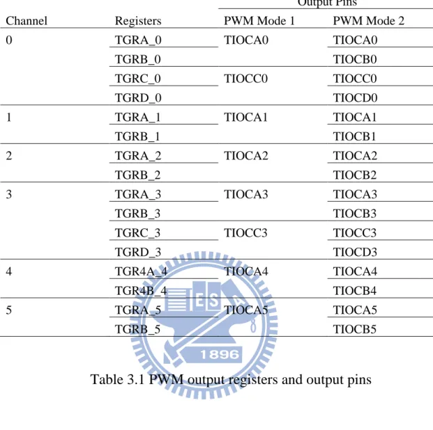
13
We use the MCU’s PWM mode 2 by setting the MD bit in TMDR, the MCU has at most 15-phase PWM output in PWM mode 2, but we only use 6
phases of them, as the following shown:
PWM output pins:
TIOCC3 – U phase (pin 28) TIOCD3 – X phase (pin 29)
TIOCA4 – V phase (pin 30) TIOCB4 – Y phase (pin 31)
TIOCA5 – W phase (pin 32) TIOCB5 – Z phase (pin 33)
We choose TPU3, TPU4 and TPU5 as our PWM timer, and setting the
SYNC3, SYNC4 and SYNC5 bit in TSTR so that we can make TPU3, TPU4 and TPU5 to be synchronized. It is necessary to set clearing source in
synchronous mode, so we let TPU3’s TGRA as our clearing source by setting TPU3’s CCLR in TCR , and it can decide the PWM’s carrier frequency. In this
thesis, we set the PWM’s carrier frequency to be 10k Hz, it is in the range of IGBT’s operation.
After setting up the PWM’s carrier frequency, we will set the duty ratio on each phase as follows (see Table 3.1):
14
TGRC_3: U phase duty ratio TGRD_3: X phase duty ratio
TGR4A_4: V phase duty ratio TGR4B_4: Y phase duty ratio
TGRA_5: W phase duty ratio TGRB_5: Z phase duty ratio
By changing the value in above registers, we can change PWM’s duty ratio
as well as we want. With IOC bits in TIORL_3, IOD bits in TIORL_3, IOA bits in TIOR_4, IOB bits in TIOR_4, IOA bits in TIOR_5, IOB bits in TIOR_5, we
can control the PWM’s duty ratio and On or Off.
3.2.3 A/D Converter
For knowing the current value, we need to read the shunt resistance voltage,
and turn the analog signal into digital signal so that the MCU can handle it. We set the SCAN bit in ADCSR register to enter scan mode and set CH bits
to 0010 to choose AN0, AN1 and AN2 channel as our A/D input pins (pin 71 ~ 73). These channels are the shunt resistance voltage’s input.
3.2.4 I/O
15
signal H1, H2 and H3 into port 1.6, port 1.5 and port 1.4.
3.3 Interrupt routine
3.3.1 RXI interrupt
When MCU received character from digital operator or PC, it will trigger
RXI interrupt to store the character.
3.3.2 TGIA0 interrupt
TGIA0 interrupt is produced by TGRA_0 compare match in TPU0, in
this interrupt, we will check the hall signal. If hall signal changes, we do the commutation job to the next step according to the six-step square commutation
table and calculating the BLDC motor’s speed by analyzing the time between steps. For better accuracy and small variation, we filter the speed and show it on
digital operator. The flowchart is shown in Fig 3.2.
3.3.3 TCIV1 interrupt
This routing is for close-loop control’s feedback. When we set up the speed
as our command, the TPU1 timer will be trigger. After the TCNT of TPU1 overflow, it will feedback speed and send it to PI controller to regulate speed.
16
3.3.4 TCIV2 interrupt
The TPU2 is used for calculating speed, it is needed to avoid the situation of stall, so we enable the TCIV2 interrupt to extend the time for calculation.
3.4 Speed estimation
According to the time between hall signal steps, speed estimation can be realized by as following formula:
)
(
)
/
(
_
rpm
Speed
s
rev
freq
timer
counter
=
×
×
×
60
24
1
1
Because we use interrupt at every 0.1ms to check the hall signal, so the speed calculated must exist error and vary in a range.
In this thesis, we take 3 steps and 6 steps time to calculate speed separately in order to reduce the error, and filter the value that we calculated to decrease
the variation, it makes the speed error to be within 1 rpm. The formula becomes:
3 step:
)
(
)
/
(
_
rpm
Speed
s
rev
freq
timer
counter
=
×
×
×
60
8
1
1
17 6 step:
)
(
)
/
(
_
rpm
Speed
s
rev
freq
timer
counter
=
×
×
×
60
4
1
1
If we take too more step to calculate speed, the frequency of updating speed will decrease, it will affect the speed response.
3.5 PI controller
For close-loop control, we use PI controller to regulate motor’s speed. The block diagram is shown in Fig 3.4. Current speed ( ) can be estimated from
hall signal, and is speed command, it is decided by digital operator.
TGRA_1 register’s compare match is used to trigger the interrupt of
checking speed variation for motor speed’s feedback. When speed changes, we feedback the new current speed value and compare to speed command to get
speed error e(k). After that, the speed error e(k) will be input to PI controller regulator, so we get the duty ratio’ value as our input . Then we renew the
duty ratio’s value in registers.
In MCU, if current speed is less than speed command, it will increase duty
ratio to accelerate, if current speed excesses speed command, it will decrease duty ratio to decelerate.
18
Chapter 4 Hardware Setup
4.1 The structure of system
Fig 4.1 is the structure of system, after rectifier the AC, it provides DC voltage to inverter, and the MCU communicates with PC and digital operator by
RS232, after downloading the program from PC, we command the BLDC motor through digital operator, and the MCU control the communication by switching
the six IGBTs’ in the inverter. With the hall sensor’s feedback to MCU, we can calculate the BLDC motor’s speed showed on digital operator. The shunt
resistance voltage is feedback to MCU too, it is used to avoid over current.
4.2 Introduction of MCU
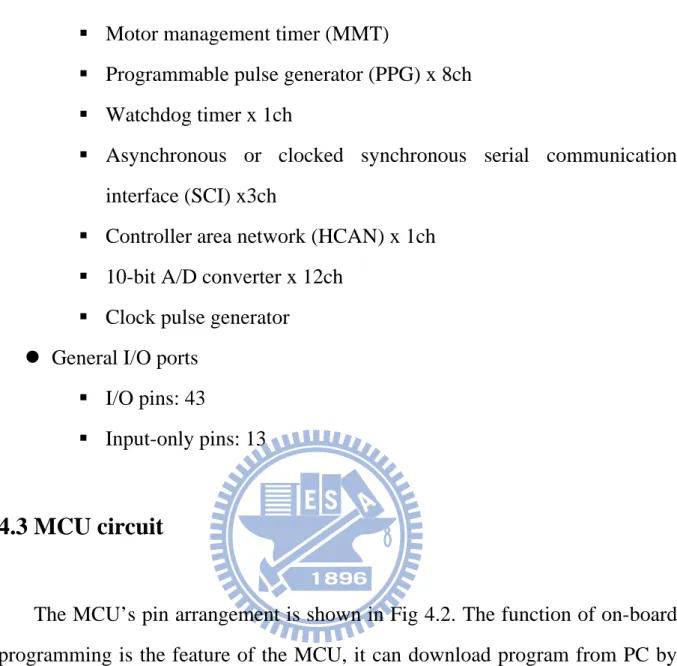
The MCU we used is H8S/2612 group produced by Renesas company, its
type is HD64F2612FA20. It has 128K ROM, 4K RAM and the ROM type is flash memory. The minimum instruction execution time is 50ns (20M Hz), and
it has 47 internal interrupt and 7 external interrupt. Its main peripheral functions are as following: Various peripheral functions
PC break controller x 2ch Data transfer controller x 85ch 16-bit timer-pulse unit (TPU) x 6ch
19
Motor management timer (MMT)
Programmable pulse generator (PPG) x 8ch Watchdog timer x 1ch
Asynchronous or clocked synchronous serial communication interface (SCI) x3ch
Controller area network (HCAN) x 1ch 10-bit A/D converter x 12ch
Clock pulse generator General I/O ports
I/O pins: 43
Input-only pins: 13
4.3 MCU circuit
The MCU’s pin arrangement is shown in Fig 4.2. The function of on-board
programming is the feature of the MCU, it can download program from PC by changing the pin state of MD2, MD1, MD0 and FWE (Flash Write Enable). See
table 4.1, if MD2, MD1, MD0 is high and FEW is low, it is in advance mode, this is normal mode, if MD1, MD0, FEW is high and MD2 is low, it is in boot
mode, this is programming mode.
Fig 4.3 is the layout of MCU circuit, the RS232 port is used to communicate
with PC. A digital operator is added to indicate the information that we need, so the left ten pins are for digital operator, the five pins below is +5V, GND and the
hall sensor’s signal input. The dip switch is used to switch between programming mode (boot mode) and normal mode (advanced mode).
20
The programming mode is working through the RxD2 and TxD2 pins, and the normal mode is working through the RxD1 and TxD1 pins, besides, the
output of the MCU’s RxD2, TxD2, RxD1, TxD1 pins and digital operator’s Rx, Tx pins are TTL signal. It is necessary to convert the TTL signal to RS232
signal so that we can communication from the MCU to PC or MCU to digital operator. Thus, we use the MX232CPE (Fig 4.4) IC to finish this job.
4.4 Digital operator
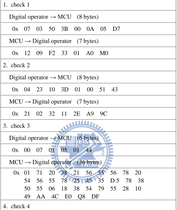
I/O is needed for a control system, we can command the motor by a digital operator shown in Fig 4.5. Table 4.2 is the digital operator’s protocol. There are
four checks in the beginning of communication, and the data format is shown in Table 4.3.
For Operator to MCU, the first two bytes are start code, and the third and forth bytes are data bytes which indicated the LED information of digital
operator. The last two bytes are the CRC (Cyclic redundancy check) code. It is a short, fixed-length binary sequence.
For MCU to Operator, the first two bytes are also start code, and the LED_Ctrl control the blink of the LED, and the LED_Data control the LED’s on
or off. After the following four null characters, the LCD_Ctrl1 and LCD_Ctrl2 affect the blink of characters which is shown in line 1 and line 2, the
LCD_Line1 and LCD_Line2 decide the content of line 1 and line 2, the last two bytes are CRC code.
21
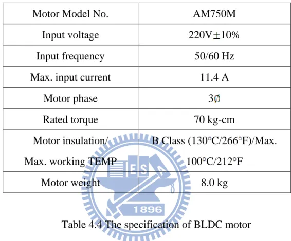
4.5 BLDC motor’s specification
Table 4.4 shows the specification of BLDC motor and Fig 4.5 shows the
BLDC motor, it is produced by Adlee Powertronic company. Its model No. is AM750M, the number means the rated output is 750W, about 1 horse power.
The last M means the rated speed is about 3000 rpm, it has U, V, W phase and the maximum input current is 11.4A.
According the motor’s hall signal and Fig 2.4, when motor runs 1/4 revolution, the hall signal changes six times, there are 24 steps in one revolution,
22
Chapter 5 Experiment
5.1 Hardware setup
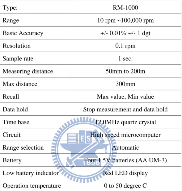
The inverter we used is shown in Fig 5.1, an IGBT module is inside and the current limit is 8A. We use tachometer to sensor the current speed in order to
compare the speed calculated by microcontroller, the tachometer’s type is RM-1000, and its specification is shown in Table 5.1.
Fig 5.2 shows the hardware setup, the experiment equipment is as following: A. PC B. Scope 1 (4 channel) C. Scope 2 (2 channel) D. Isolation transformer 1 E. Isolation transformer 2 F. Auto-transformer G. Inverter H. Digital operator I. BLDC motor J. Tachometer
The isolation transformer is needed to isolate MCU and computer from the power source for safety, and the auto transformer is used to boost 110V AC to
23
220V AC and provide to inverter.
5.2 Experiment result
Fig 5.3 shows the six-step waveform at 1000 rpm, and Fig 5.4 shows its hall
signal’s waveform, according to Fig 5.4, the each step time is about 2.5ms, so the speed can be calculated as follow:
)
(
)
/
(
.
5
ms
24
rev
s
60
1000
rpm
2
1
×
=
×
So the experiment result is the same as theory.
At this experiment, we use 3 step and 6 step’s time to calculate speed
separately, and compare it to tachometer to get speed error. The speed error is shown in Fig 5.5. The result indicates that the 6 step is better and speed error is
within 0.2 rpm,
The speed response without load at 1000 rpm and 3000 rpm is shown in Fig
5.6 and Fig 5.7, we record the process of experiment and take the every moment of speed and time when speed changed, after gathering these points, we can plot
the waveform as shown.
The dash line is command and the plus mark is the response of parameter
Kp = 0.03 and Ki = 0.1, the circle mark is the response of parameter Kp = 0.03 and Ki = 0.05. Both the response time are about 5 to 6 second.
The star mark is the response of Adlee driver, it is used to make comparison. The specification of Adlee driver is shown in Table 5.2.
24
Fig 5.8 shows the speed response with load at 500 rpm. So as figure shown, the response of parameter Kp = 0.03 and Ki = 0.05 is good than Adlee driver.
25
Chapter 6 Conclusion
According to the experiment result, we can find that the response is faster
and the overshoot may exist when Ki become decrease.
In the experiment, we have some problems when we implement the BLDC
motor control and make it failure. The failure analysis list as following:
1. Isolation
Fig 5.2 shows the hardware setup. At first, we did not add the isolation transformer, so the computer’s ground and the inverter’s ground
are the same. It will cause damage to computer and microcontroller. Besides, the primary and secondary’s ground of flyback converter in the
inverter are conncected, it will also ruin computer or microcontroller.
2. PWM output waveform
When we set up the PWM output pin by TIOR (Timer input/output control register), the output pins state are right at beginning, but after
four to five times of switching PWM output pins state, the output waveforms are error. This is caused by wrong setting so that we ruin
many IGBT module in the inverter. So the pins state need to check carefully.
26
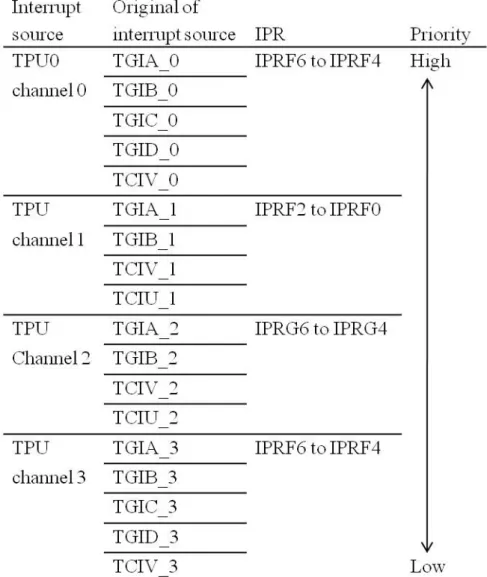
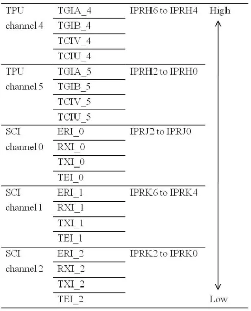
3. Priority
In the experiment, the interrupt of checking hall signal and doing commutation must be the highest priority in the interrupts we used, if
this interrupt be affected, we have chance to break IGBT module. Table 6.1 shows the priority of internal interrupt, so TGIA_0 interrupt is used
for checking hall signal.
The MCU we used is powerful, it can be used to develop more complex control method in BLDC motor such as direct torque control.
27
Reference
[1] Y. S. Lai, F. S. Shyu, and Y. H. Chang, “Novel loss reduction pulse width
modulation technique for brushless dc motor drives fed by MOSFET inverter”, IEEE Trans. Power Electron., vol. 19, no. 6, pp. 1646-1652, Nov. 2004.
[2] K. Y. Cheng and Y. Y. Tzou, “Design of a sensorless Commutation IC for BLDC Motors”, IEEE Transactions of Power Electronics, vol.18, no.6,
pp.1365-1375, November 2003.
[3] H. C. Chen, Y. C. Chang, and C. K. Huang, “Practical sensorless control for
inverter-fed BDCM compressors,” IET Proc. Electric Power Applications, vol. 1, no. 1,pp. 127-132, Jan. 2007. [4] 徐舶強, 無感測直流無刷馬達之驅動電路設計, 國立交通大學機械工程學 系所, 碩士論文, 2008 [5] 吳宇中, 使用微控制器SN8P1708晶片實現三相永磁馬達之控制, 國立交通 大學電機與控制工程系所, 碩士論文, 2005 [6] 賴逸軒, 以DSP為基礎發展永磁同步馬達使用線性型霍爾感測器與無感測 控制方法, 交通大學電機與控制工程系所, 碩士論文, 2005 [7] 卓淑婷, 直流無刷馬達無感測器驅動之分析, 交通大學電機與控制工程系 所, 2009
28
Table
Step Electrical angle Phase current Hall sensor Switch on
1 100 Q5, Q0 2 101 Q3, Q0 3 001 Q3, Q4 4 011 Q1, Q4 5 010 Q1, Q2 6 110 Q5, Q2
29
Output Pins
Channel Registers PWM Mode 1 PWM Mode 2
0 TGRA_0 TIOCA0 TIOCA0
TGRB_0 TIOCB0
TGRC_0 TIOCC0 TIOCC0
TGRD_0 TIOCD0
1 TGRA_1 TIOCA1 TIOCA1
TGRB_1 TIOCB1
2 TGRA_2 TIOCA2 TIOCA2
TGRB_2 TIOCB2
3 TGRA_3 TIOCA3 TIOCA3
TGRB_3 TIOCB3
TGRC_3 TIOCC3 TIOCC3
TGRD_3 TIOCD3
4 TGR4A_4 TIOCA4 TIOCA4
TGR4B_4 TIOCB4
5 TGRA_5 TIOCA5 TIOCA5
TGRB_5 TIOCB5
Table 3.1 PWM output registers and output pins
MD2 MD1 MD0 FWE LSI state after Reset end
1 1 1 0 Advance Mode
0 1 1 1 Boot Mode
30
1. check 1
Digital operator → MCU (8 bytes)
0x 07 03 50 3B 00 0A 05 D7
MCU → Digital operator (7 bytes) 0x 12 09 F2 33 01 A0 M0
2. check 2
Digital operator → MCU (8 bytes)
0x 04 23 10 3D 01 00 51 43
MCU → Digital operator (7 bytes) 0x 21 02 32 11 2E A9 9C
3. check 3
Digital operator → MCU (6 bytes) 0x 00 07 01 05 01 44
MCU → Digital operator (36 bytes)
0x 01 71 20 38 21 56 55 56 78 20 54 56 55 78 25 45 35 D 5 78 38 50 55 06 18 38 54 79 55 28 10 49 AA 4C E0 Q8 DF
4. check 4
Digital operator → MCU (6 bytes) 0x 04 78 51 10 C6 4F
MCU → Digital operator (46 bytes)
0x 22 25 38 44 44 7E 45 44 3C 40 42 43 3C 3C 40 42 21 6C 3C 41 40 43 AC 20 55 56 54 98 38 45 56 54 14 38 46 45 56 68 73 FD 20 01 03 A0 30 50
31
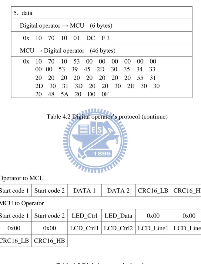
5. data
Digital operator → MCU (6 bytes) 0x 10 70 10 01 DC F 3
MCU → Digital operator (46 bytes)
0x 10 70 10 53 00 00 00 00 00 00 00 00 53 39 45 2D 30 35 34 33 20 20 20 20 20 20 20 20 55 31 2D 30 31 3D 20 20 30 2E 30 30 20 48 5A 20 D0 0F
Table 4.2 Digital operator’s protocol (continue)
Operator to MCU
Start code 1 Start code 2 DATA 1 DATA 2 CRC16_LB CRC16_HB
MCU to Operator
Start code 1 Start code 2 LED_Ctrl LED_Data 0x00 0x00
0x00 0x00 LCD_Ctrl1 LCD_Ctrl2 LCD_Line1 LCD_Line2
CRC16_LB CRC16_HB
32
Motor Model No. AM750M
Input voltage 220V 10%
Input frequency 50/60 Hz
Max. input current 11.4 A
Motor phase 3
Rated torque 70 kg-cm
Motor insulation/ Max. working TEMP
B Class (130 C/266 F)/Max. 100 C/212 F
Motor weight 8.0 kg
33
Type: RM-1000
Range 10 rpm ~100,000 rpm
Basic Accuracy +/- 0.01% +/- 1 dgt
Resolution 0.1 rpm
Sample rate 1 sec.
Measuring distance 50mm to 200m
Max distance 300mm
Recall Max value, Min value
Data hold Stop measurement and data hold
Time base 12.0MHz quartz crystal
Circuit High speed microcomputer
Range selection Automatic
Battery Four 1.5V batteries (AA UM-3)
Low battery indicator Red LED display
Operation temperature 0 to 50 degree C
Table 5.1 Specification of tachometer
34
35
36
Figure
Fig 2.1 The structure of BLDC motors
I B d + _ VH
37
Fig 2.3 Schematic of the inverter and motor
38
Step 1
Step 2
Step 3
39
Step 4
Step 5
Step 6
40 + _ + _ + _ ea eb R ec R R L L L a b c ia ib ic n
Fig 2.6 The equivalent model of a BLDC motor
E PWM I Vs Vce + _ Ra
41
42
43 H1
H2 H3
1 hall step or 1 pulse
Fig 3.3 Hall signal
Fig 3.4 Close-loop control block diagram
44
Fig 4.2 The HD64F2612F340 chip’s pin arrangement
45
Fig 4.4 MAX232CPE
46
Fig 5.1 Inverter
47
48
Fig 5.4 Hall signal’s waveform
49
Fig 5.5 Speed error (continue)
50
Fig 5.7 Speed response without load at 3000 rpm