國 立 交 通 大 學
電子工程學系 電子研究所碩士班
碩士論文
低溫複晶矽薄膜電晶體
其結晶方式與新穎結構之研究
The Study of Crystallization Schemes and Novel
Structures in Low Temperature Poly-Si
Thin-Film Transistors
研 究 生:張哲綸
指導教授:雷添福 博士
低溫複晶矽薄膜電晶體其結晶方式與新穎結構之研究
The Study of Crystallization Schemes and Novel
Structures in Low Temperature Poly-Si
Thin-Film Transistors
研 究 生:張哲綸 Student: Che-Lun Chang 指導教授:雷添福 博士 Advisor: Dr. Tan-Fu Lei
國 立 交 通 大 學
電子工程學系 電子研究所碩士班
碩士論文
A Thesis
Submitted to Department of Electronics Engineering & Institute of Electronics College of Electrical Engineering & Computer Engineering
National Chiao Tung University In Partial Fulfillment of the Requirements
For the Degree of Master of Science
in
Electronic Engineering June 2007
Hsinchu Taiwan Republic of China
低溫複晶矽薄膜電晶體其結晶方式與新穎結構
之研究
學生: 張哲綸
指導教授: 雷添福 博士
國立交通大學
電子工程學系 電子研究所碩士班
摘 要
在本論文中,首先,我們研究利用氬氣(Argon)的離子佈植去改善複晶矽薄 膜電晶體的特性,透過這種新穎的表面成核機制,不但會使複晶矽的結晶顆粒變 大而且結晶的缺陷也會被抑制住而變少,因此,我們能得到高品質的複晶矽通 道,我成功地將氬氣離子佈植的薄膜電晶體做出來而且我的實驗結果顯示和傳統 薄膜電晶體相較之下它有很好的場效載子移動率(46.06 cm2/Vs)和低密度的晶粒邊界補陷能階(grain boundary trap state)(3.44 × 1012 cm-2)。
接著,我們進行懸浮通道複晶矽薄膜電晶體的研究,在第 3 章中我們將看 到此種元件有很好的電特性。懸浮通道薄膜電晶體和傳統元件相較之下有200% 的電特性改善,這是因為我們使用的結晶成核機制不同於傳統,使得結晶顆粒變 大且缺陷變少,因此我們得到一個高品質的通道層而這種新式結構非常適合應用 在未來高性能大面積元件製程中。 最後,我們研究利用間隙壁(spacer)技術來做
複
晶矽薄膜電晶體的奈米線通 道,此種元件結構的特色就是在你定義的線條側壁上留下自動對準的複晶矽奈米線通道,這種成對式奈米線通道元件有很好的閘極控制能力因為它的結構類似三
閘極式結構,而且也因為它的通道是奈米線使得
複
晶矽的晶粒邊界缺陷被抑制住,因此,這種元件有很好的電特性如有較高的ON/OFF 電流比(>107),不錯的
The Study of Crystallization Schemes and Novel
Structures in Low Temperature Poly-Si
Thin-Film Transistors
Student: Che-Lun Chang
Advisor: Dr. Tan-Fu Lei
Department of Electronics Engineering &
Institute of Electronics
National Chiao Tung University
ABSTRACT
In this thesis, first, we studied Enhanced performance of poly-silicon thin-film transistors (poly-Si TFTs) with Argon ion implantation. By adopting this novel surface-nucleation solid-phase-crystallization scheme, not only the grain size of poly-Si can be increased but also the intragranular defects can be suppressed effectively. Therefore, a high quality poly-Si film within the channel with better crystallinity is formed. Argon-implanted TFTs have been successfully fabricated and the experimental results demonstrate a superior field-effect mobility of 46.06 (cm2/Vs), a fewer grain boundary trap state densities of 3.44 x10¹² (cm-2) than those of conventional TFTs.
Then, Floating channel polycrystalline silicon thin-film transistors are studied and demonstrated having superior electrical characteristics in the Chapter 3. In comparing with the conventional TFTs, the fabricated floating channel TFTs has an
electrical property about 200% improved. The achievement is highly attributed to the fact that, by adopting this novel crystallization scheme, both the grain size and the intragranular defects of polycrystalline silicon are effectively improved. Therefore, we have demonstrated here a promising structure which forms a high quality channel film and is especially suitable for the future high-performance large-area device applications.
Finally, the electrical characteristics of thin-film transistors (TFTs) with poly-Si nanowire (NW) channels fabricated by a novel sidewall spacer technique are studied. The new device features a conventional planar structure with self-aligned poly-Si NW channels along the sidewall of the prepatterned dummy stripe. The proposed TFT with twin nanowire channels owns outstanding gate controllability owing to its three-dimensional tri-gate-like structure, and holds suppressed poly-Si grain bounday defects owing to its nanoscale dimension. Therefore, the fabricated NW TFT exhibits excellent electrical characteristics, such as a high ON/OFF current ratio (>107), a reasonable subthreshold swing (S.S.) of 395 mV/decade. These results suggest that the fabrication procedure of NW TFT is a very promising candidate for future practical manufacturing.
誌謝
首先誠摯的感謝指導教授雷添福博士,老師悉心的教導使我得以一窺 領域的深奧,不時的討論並指點我正確的方向,使我在這兩年中獲益匪 淺,老師對學問的嚴謹更是我輩學習的典範。兩年的研究生涯中,不僅僅只 是學習到做研究的精神與方法,老師的關心、鼓勵與啟發,使我在面對將來漫長 的人生旅途,受用無窮。 再者,我要特別感謝張家文學長,學長不僅在研究過程中都很熱心地幫助 我、指導我,在日常生活中也都特別的關心照顧我。另外要感謝黃俊嘉學長在實 驗上經驗的傳承,還有楊學長、陳建豪學長、郭柏儀學長、陳志仰學長、馬鳴汶 學長、統億學長、錦石學長,感謝你們這些日子以來的關心與指導。也要感謝久 騰、明爵、仕傑、統億、文呈、冠良、文彥、子恆、張婷、春瑀,懷念與你們相 處的日子以及一起討論課業時的那股求知的熱情。 最後,我要感謝我最親愛的家人,在我追學過程中一直的全力支持我,給我 最大的支持與鼓勵,僅以此論文獻予你們。Contents
Abstract (Chinese) ………I
Abstract (English) ………..III
Acknowledge ………V
Contents ………..VI
Table & Figure Captions .………...VIII
Chapter 1 Introduction ……….1
1.1 Overview of Poly-Si Thin-Film Transistors ....………...1
1.2 Motivation ……….………..……...3
1.3 Method of Device Parameter Extraction ………...………….5
1.3.1 Determination of Threshold Voltage ………...6
1.3.2 Determination of Subthreshold-Swing .………..……..….7
1.3.3 Determination of Field Effect Mobility..………..……...7
1.3.4 Determination of ON/OFF Current Ratio .……….…...…....8
1.3.5 Extraction of Grain Boundary Trap State Density..……….…..…....9
1.4 Organization of the Thesis………...….10
References ……….……….…12
Chapter 2 The Study of Ar Ion Implantation to Enhance Solid Phase Crystallization in Poly-Si TFT
s
………....………...172.1 Introduction ……….………...…..17
2.2 Experimental..………...…………...………...…………..18
2.3 Results and Discussion………...………..19
2.4 Summary ……….……….…22
Chapter 3 High-Performance Poly-Si TFTs Fabricated by Floating Channel
Solid-Phase-Crystallization Technique……….………..…………..38
3.1 Introduction ………..38
3.2 Experimental ………..………..39
3.3 Results and Discussion ……….40
3.4 Summary ………...………...42
References ……….……….43
Chapter 4 A Novel Spacer Technique to Fabricate Poly-Si TFTs with Twin Sub-100-nm Nanowire Channels………...………....54
4.1 Introducion ……….………..54
4.2 Experimental …...……….………55
4.3 Results and Discussion ……….56
4.4 Summary ...………...57
References ……..………58
TABLE CAPTIONS
Chapter 2
Table 2-1 Comparison of device characteristics of the conventional and the Argon implanted poly-Si TFTs.
Chapter 3
Table 3-1 Comparison of device characteristics of the CN and the FC poly-Si TFTs.
FIGURE CAPTIONS
Chapter 2
Fig. 2-1 Schematic diagram of fabrication process for the Argon implanted poly-Si TFTs
Fig. 2-2 SEM images of the conventional and the Argon implanted poly-Si films Fig. 2-3 XRD patterns of the poly-Si film for the Argon-implanted and the
conventional samples after SPC annealing
Fig. 2-4 Transfer characteristics and field effect mobility of the conventional and the Argon implanted poly-Si TFTs with VD = 0.5V , 5V
Fig. 2-5 Output characteristic of the conventional and the Argon implanted poly-Si TFTs
Fig. 2-6 Trap state density extraction of the conventional and the Argon implanted poly-Si TFTs
Fig. 2-7 Threshold voltage variation with stress time under hot-carrier stress Fig. 2-8 On-current degradation with stress time under hot-carrier stress
Chapter 3
Fig. 3-1 Process flow of the FC poly-Si TFTs
Fig. 3-2 Topological layout , 3-D structure and Cross-section views of the CN TFTs and the proposed FC TFTs
Fig. 3-3 TEM image of the FC poly-Si TFTs
Fig. 3-4 SEM images of the CN and the FC poly-Si films
Fig. 3-5 Transfer characteristics and field effect mobility of the conventional and the floating channel poly-Si TFTs with VD = 0.5V , 3V
channel (FC) poly-Si TFTs
Fig. 3-7 Trap state density extraction of the CN and the FC poly-Si TFTs
Chapter 4
Fig. 4-1 Schematic diagram of fabrication process and top view of the mask layout for the proposed NW TFTs
Fig. 4-2 Cross-sectional profile by transmission electron microscope (TEM) Fig. 4-3 The atomic force microscope (AFM) image of the twin poly-Si NW Fig. 4-4 Transfer characteristics of the NW poly-Si TFTs with VD = 0.5V , 3V
Chapter 1
Introduction
1.1
Overview of Low Temperature Poly-Si Thin-Film Transistors
The study of polycrystalline silicon (poly-Si) thin film transistors (TFTs) fabricated using a maximum temperature below 600oC commenced until 1980s. We defined this kind of poly-Si TFTs as Low temperature polysilicon thin film transistors (LTPS-TFTs) . It have received much attention in recent years because of their applications , such as active matrix liquid crystal displays (AMLCDs) [1-3] , active matrix organic light emitting displays (AMOLEDs) [4-6] , high density static random access memories (SRAMs) [7], electrical erasable programming read only memories (EEPROM) [8][9] and candidate for 3-dimenstion ICs’ applications [10] . Within those applications, the application of active matrix liquid crystal displays (AMLCDs) is the major driving force to promote the developments of poly-Si TFT technology .
The first generation of active matrix liquid crystal displays (AMLCDs) used a-Si:H TFTs for the pixel switching device. The advantages of a-Si:H TFTs are their compatibility with low processing temperature on large-area glass substrates and low leakage current due to the high off-stated impedance. However , the low electron field-effect mobility(<1 cm2/Vs) has limited the development of AMLCDs technology. So , the poly-Si TFTs acted important role for AMLCDs development , because the high field effect mobility and the high driving current of poly-Si TFTs makes the integration of switching pixels and driver circuits possible [11]. Moreover, the aperture ratio and the panel brightness can be also greatly promoted due to small
device size needed using poly-Si TFTs [12]. Therefore, the performance of display can be significantly improved. So polysilicon films crystallized from amorphous silicon have been of great interest for active layers in the thin film transistors (TFTs), which are used to drive and switch the image pixels in active matrix liquid crystal displays (AMLCDs) and also used in silicon-on-insulator (SOI) technologies for three-dimensional integrated devices[13].The electrical characteristics of polysilicon TFTs are strongly dependent on the polysilicon microstructure. Grain boundaries and intragranular defects are electrical potential barriers and scattering sites, which decrease the carrier transport mobility and also serve as midgap states to increase the leakage currents. Polysilicon films with larger grain sizes and fewer intragranular defects have been a continual goal[14]–[17].Recent low temperature (<600°C) solid phase crystallization (SPC) techniques propose that the grain size and the mobility are not good enough , even though there should be no grain boundaries within the channel. However, the residual intragranular defects reduce the defect-free area of polysilicon film down to 30 nm, and it is thought that they become the limiting factor in device performance[18]. Therefore, reducing the density of intragranular defects becomes very important to improve the electrical performance of TFTs. To date, two methods have been suggested to reduce the density of intragranular defects: high-temperature annealing[18][19]and laser crystallization[20].Haji et al.[18] reported that main intragranular defects in polysilicon films after crystallization at 600°C are microtwins, that they are not stable above 750°C, and that they can be eliminated after further high-temperature annealing. However, high-temperature processing cannot be applied to AMLCD TFTs fabricated on glass substrates with a strain point less than 650 °C. Compared with the furnace annealing, laser crystallization has disadvantages of high cost and poor film uniformity. Reducing this intragranular defect density of SPC polysilicon films at a temperature below 650°C is a motivating factor for this
research.
As compared with single crystalline silicon, the polycrystalline Silicon may consist of many grains, whose boundaries are composed of unsatisfied dangling silicon bonds that may trap charge carriers and become charged. This results in the formation of potential barriers between grains and also between the grain interior and its boundary [21]. The major effect of grain boundaries and intra-grain defects on the electrical performance of a TFT results from lowering the carrier mobility. This results in a degradation of drive current and subthreshold swing , and increases the threshold voltage, leakage current, and the temperature dependence of the device[21][22]. In order to obtain desirable electrical characteristics of poly-Si TFTs , several methods have been proposed to improve the device performance by enlarging the grain size of poly-Si films[23][24] and reducing the trap states in grain boundaries . Many crystallization techniques have been proposed to achieve low temperature polycrystalline silicon (LTPS) TFTs , such as SPC (solid phase crystallization)[25] , ELA (excimer laser annealing)[26][27] and MILC (metal induced lateral crystallization)[28]. Plasma treatments is also a method for reducing trap states in grain boundaries, various plasmas such as H2 [29], NH3 [30], N2O[31]
and O2 plasmas [32] have been intensely investigated in recent years.
Moreover, the device performance could also be improved by adopting novel device structures. Offset drain/source [33], Lightly doped drain (LDD) [34], gate overlapped LDD [35] , multiple channel structure [36] , Double or multiple gate structures [37], vertical channel [38] have been proposed and investigated intensively.
1.2
Motivation
mobility of poly-Si TFTs. This is because we want to gain higher on-current for AMLCD applications. Thus, the aperture ratio will be increased and then brightness will certainly increase. In recent years, the poly-Si TFTs have many applications which not only AMLCD but also 3-d circuit applications are very popular. We enhanced mobility of poly-Si TFTs can help system and circuit designer having wide window to design.
First, we have proposed that using Argon ion implantation to enhance mobility. Polycrystalline silicon (poly-Si) is an attractive material for use in large-area electronics, such as thin film transistors (TFTs), solar cells, and image sensors, because of its high carrier mobility compared with amorphous silicon (a-Si).It is believed that electrical properties of the TFT’s can be improved if the grain size can be enhanced and the number of grain boundaries in the channel region can be minimized. Solid-phase crystallization (SPC) annealing in a furnace is a widely used scheme because of its simplicity as well as its ability to produce a smooth interface and excellent uniform film [39].Unfortunately, the traditionally SPC methods which was began a nucleation of Si atoms from bounded a-Si film interface (a-Si/SiO2)
obtain the poly-Si film and therefore lead to smaller grain size [40]-[42].Because of this the nucleation of Si atoms from the free top surface of a-Si film is proposed to improve the quality of SPC poly-Si film. So, we proposed Solid Phase Crystallized Poly-Si TFTs with Argon ion implantation to achieve the nucleation mechanism.
Then, floating channel polycrystalline silicon thin-film transistors are proposed and demonstrated having superior electrical characteristics in the Chaper 3. It is well known that the electrical characteristics of poly-Si TFTs are strongly correlated to the microstructure of poly-Si film. In the channel, the grain boundaries and intragranular defects act as scattering centers and midgap traps to degrade the electrical characteristics. Unfortunately, the traditionally SPC methods which was began a
nucleation of Si atoms from bounded a-Si film interface (a-Si/SiO2) obtain the poly-Si
film and therefore lead to smaller grain size. Because of the floating channel without bounded interface issue the poly-Si flim can achieve bigger grain size to enhance the electrical characteristics. The achievement is highly attributed to the fact that, by adopting this novel crystallization scheme, both the grain size and the intragranular defects of polycrystalline silicon are effectively improved. So, we proposed floating channel poly-Si TFTs to improve device performance.
Finally, the electrical characteristics of thin-film transistors (TFTs) with solid-phase crystallization (SPC) poly-Si nanowire (NW) channels fabricated by a novel sidewall spacer technique are proposed. The new device features a conventional planar structure with self-aligned poly-Si NW channels along the sidewall of the prepatterned dummy stripe. The proposed TFT with twin sub-100 nm linewidth channels owns outstanding gate controllability owing to its three-dimensional tri-gate-like structure, and holds suppressed poly-Si grain bounday defects owing to its nanoscale dimension. Using this method to produce a nearly three-dimensional tri-gate-like profile doesn’t need costly photolithography process like electron- beam lithography (EBL) techniques. This method is therefore simple, low-cost, and process-compatible with modern semiconductor manufacturing processes. So TFTs with SPC poly-Si nanowire (NW) channels fabricated by a novel sidewall spacer technique is a very promising candidate for future practical manufacturing.
1.3 Method of Device Parameter Extraction
In this thesis, all of the electrical characteristics of proposed poly-Si TFTs were measured by HP 4156B-Precision Semiconductor Parameter Analyzer.
Many methods have been proposed to extract the characteristic parameters of poly-Si TFTs. In this section, those methods are described.
1.3.1 Determination of Threshold Voltage
Threshold voltage (Vth) is an important parameter required for the channel
length-width and series resistance measurements. However, Vth is not uniquely
defined. Various definitions have been proposed and the reason can be found in ID-VGS curves. One of the most common techniques is the linear extrapolation method
with the drain current measured as a function of gate voltage at a low drain voltage of 50~100mV to ensure operation in the linear region [43]. The drain current is not zero when VGS below threshold voltage and approaches zero asymptotically. Hence the IDS
versus VGS curve can be extrapolated to ID=0, and the Vth is determined from the
extrapolated intercept of gate voltage (VGSi) by
2 DS GSi th V V V = − --- (Eq. 1.1)
Equation (1.1) is strictly only valid for negligible series resistance. Fortunately series resistance is usually negligible at the low drain current when threshold voltage measurements are made. The IDS-VGS curve deviates from a straight line at gate
voltage below Vth due to subthreshold current and above Vth due to series resistance
and mobility degradation effects. It is common practice to find the point of maximum slope of the IDS-VGS curve and fit a straight line to extrapolate to ID=0 by means of
finding the point of maximum of transconductance (Gm).
In this thesis, we use a simpler method to determinate the Vth called constant
drain current method. The voltage at a specified threshold drain current is taken as the Vth. This method is adopted in the most studied papers of poly-Si TFTs. It can be
given a threshold voltage close to that obtained by the complex linear extrapolation method. Typically, the threshold current is specified at (W/L) × 10nA for VDS = 0.1V
length, respectively.
1.3.2 Determination of Subthreshold Swing
Subthreshold swing (S.S.) is a typical parameter to describe the control ability of gate toward channel, which reflects the turn on/off speed of a device. It is defined as the amount of gate voltage required to increase/decrease drain current by one order of magnitude.
The S.S. should be independent of drain voltage and gate voltage. However, in reality, the S.S. increases with drain voltage due to channel shortening effect such as charge sharing, avalanche multiplication and punchthrough effect. The subthreshold swing is also related to gate voltage due to undesirable and inevitable factors such as the serial resistance and interface states.
In this thesis, the S.S. is defined as one-third of the gate voltage required to decrease the threshold current by three orders of magnitude. The threshold current is specified to be the drain current when the gate voltage is equal to threshold voltage.
1.3.3 Determination of Field Effect Mobility
Usually, field effect mobility (μeff) is determined from the maximum value of transconductance (Gm) at low drain bias. The transfer characteristics of poly-Si TFTs are similar to those of conventional MOSFETs, so that the first order of I-V relation in the bulk Si MOSFETs can be applied to poly-Si TFTs. The drain current in linear region (VDS<VGS-Vth) can be approximated as the following equation:
(
)
⎥⎦⎤ ⎢⎣ ⎡ − − ⎟ ⎠ ⎞ ⎜ ⎝ ⎛ = 2 2 1 DS DS th GS ox eff DS V V V V L W C I μ --- (Eq. 1.2)oxide capacitance per unit area and Vth is the threshold voltage. Thus, the transconductance is given by DS ox eff GS DS m V L W C V I g ⎟ ⎠ ⎞ ⎜ ⎝ ⎛ = ∂ ∂ = μ --- (Eq. 1.3)
Therefore, the field-effect mobility is
(max) →0 = DS V m DS ox eff g WV C L μ --- (Eq.1.4)
1.3.4 Determination of ON/OFF Current Ratio
On/off current ratio is one of the most important parameters of poly-Si TFTs since a high-performance device exhibits not only a large on-current but also a small off-current (leakage current). The leakage current mechanism in poly-Si TFTs is not like that in MOSFET. In MOSFET, the channel is composed of single crystalline Si and the leakage current is due to the tunneling of minority carrier from drain region to accumulation layer located in channel region. However, in poly-Si TFTs, the channel is composed of poly-Si. A large amount of trap state densities in grain structure attribute a lot of defect states in energy band gap to enhance the tunneling effect. Therefore, the leakage current is much larger in poly-Si TFTs than in MOSFET. When the voltage drops between gate voltage and drain voltage increases, the band gap width decreases and the tunneling effect becomes much more severe. Normally we can find this effect in typical poly-Si TFTs’ IDS-VGS characteristics where the
magnitude of leakage current will reach a minimum and then increase as the gate voltage decreases/increases for n/p-channel TFTs.
There are a lot of ways to specify the on and off-current. In this chapter, take n-channel poly-Si TFTs for examples, the on-current is defined as the drain current when gate voltage at the maximum value and drain voltage is 5V. The off-current is specified as the minimum current when drain voltage equals to 5V.
V V at Plot V I of Current Minimum V V at Plot V I of Current Maximum I I DS GS DS DS GS DS OFF ON 5 5 = − = − = --- (Eq. 1.5)
1.3.5 Extraction of Grain Boundary Trap State Density
The Trap State Density (Nt), which can be determined by the theory established
by Levinson et al. [44], which is based on Seto’s theory [45].
For poly-Si TFTs, the drain current IDS can be given as following:
⎟ ⎟ ⎠ ⎞ ⎜ ⎜ ⎝ ⎛ − ⎟ ⎠ ⎞ ⎜ ⎝ ⎛ = GS ox Si c t GS DS ox FE DS V kTC L N q V V L W C I ε μ 8 exp 2 3 --- (Eq. 1.6) Where,
μeff field-effect mobility of carriers q electron charge
k Boltzmann’s constant εSi dielectric constant of silicon T temperature
Nt trap-state density per unit area Lc channel thickness
This expression, first developed by Levinson et al., is a standard MOSFET’s equation with an activated mobility, which depends on the grain-boundary barrier height. Levinson et al. assumed that the channel thickness was constant and equal to the thickness of the poly-Si film (t). This simplifying assumption is permissible only for very thin film (t<10nm). The trap-state density can be obtained by extracting a straight line on the plot of ln(IDS/VGS) versus 1/VGS at low drain voltage and high gate
voltage.
Proano et al. [46] thought that a barrier approximation is to calculate the gate induced carrier channel thickness by solving Poisson’s equation for an undoped material and to define the channel thickness (Lc) as a thickness in which 80% of the
(
)
fb GS SiO Si ox c V V q kTt L − = 2 8 ε ε --- (Eq. 1.7)which varies inversely with (VGS−Vfb). This predicts, by substituting Eq.1.7 into
Eq.1.6, that ln[IDS/(VGS−Vfb)] versus 1/(VGS−Vfb)2. We use the gate voltage at which
minimum leakage current occurs as flat-band voltage (Vfb). Effective trap-state
density (Nt) can be determined from the square root of the slope.
1.4 Organization of the Thesis
In the following sections, we will show our research efforts.
In Chapter 2, the electrical characteristics and fabrication processes of poly-Si TFTs with Argon ion implantation will be proposed. Experimental results reveal that the performance and reliability of our devices have remarkable improvements in comparison with conventional TFTs. Additionally, we make a detail discussion to explain the results of experimental.
In Chapter 3, the fabrication processes and electrical characteristics of Floating channel polycrystalline silicon thin-film transistors will be proposed. Experimental results reveal that poly-Si TFTs with floating channel have better performance than the conventional TFTs. Then, we will make a complete discussion about the electrical characteristics of poly-Si TFTs with floating channel.
In Chapter 4, he fabrication processes and electrical characteristics of TFTs with SPC poly-Si nanowire (NW) channels fabricated by a novel sidewall spacer technique will be proposed. Experimental results reveal that poly-Si TFTs with NW channel fabricated by a novel sidewall spacer technique is simple, low-cost, process-compatible with modern semiconductor manufacturing processes and has good electrical characteristics. Then, we will make a complete discussion about the
electrical characteristics of our devices.
References:
[1] Y. Oana, “Current and future technology of low-temperature poly-Si TFT-LCDs,”
Journal of the SID, vol. 9, pp. 169-172, 2001.
[2] S. Morozumi, K. Oguchi, S. Yazawa, Y. Kodaira, H. Ohshima, and T. Mano, “B/W and color LC video display addressed by poly-Si TFTs,” SID Dig., pp.156, 1983. [3] R. E. Proano, R. S. Misage, D. Jones, and D. G. Ast, “Guest-host active matrix
liquid-crystal display using high-voltage polysilicon thin film transistors,” IEEE
Trans. Electron Devices, vol. 38, pp. 1781, 1991.
[4] Mark Stewart, Robert S. Howell , Leo Pires, Miltiadis K. Hatalis, Webster Howard, and Olivier Prache, “Polysilicon VGA active matrix OLED displays – technology and performance”, in IEDM tech, Dig., pp.871-874, 1998.
[5] Mark Stewart, Robert S. Howell , Leo Pires, Miltiadis K. Hatalis, “Polysilicon TFT technology for active matrix OLED displays,” IEEE Trans. Electron Devices, vol. 48,pp.845-851,2001.
[6] Zhiguo Meng and Man Wong, “Active-matrix organic light-emitting diode displays realized using metal-induced unilaterally crystallized polycrystalline silicon thin-film transistors,” IEEE Trans. Electron Devices, vol.49,pp. 991-996,2002.
[7] S. Batra, “Development of drain-offset (DO) TFT technology for high density SRAM’s,” Extended Abstracts, vol.94-2, in Electrochemical Soc. Fall Mtg.,
Miami Beach, FL, Oct. pp. 677,1994.
[8] M. Cao, et al., “A simple EEPROM cell using twin polysilicon thin-film transistors,” IEEE Trans. Electron Devices, vol. 15, pp. 304, 1994.
[9] N. D. Young, G. Harkin, R. M. Bunn, D. J. McCulloch, and I. D. French, “The fabrication and characterization of EEPROM arrays on glass using a low
temperature poly-Si TFT process,” IEEE Trans. Electron Devices, vol. 43, pp. 1930-1936, 1996.
[10] K. Banerjee, S. J. Souri, P. Kapur, and K. C. Saraswat, “3-D ICs: a novel chip design for improving deep-submicrometer interconnect performance and system-on-chip integration,” Proceedings of the IEEE, vol.89, pp. 602-633, 2001.
[11] W. G. Hawkins, “Polycrystalline-Silicon device technology for large-area electronics,” IEEE Trans, Electron Devices, vol. 33, pp. 477-481, 1986.
[12] I. –W. Wu, “Cell design considerations for high-aperture-ratio direct-view and projection polysilicon TFT-LCDs,” in SID Tech. Dig., pp. 19, 1995.
[13] S. D. S. Malhi et al., IEEE Trans. Electron Devices 32, 258, 1985. [14] K. Nakazawa, J. Appl. Phys. 69, 1703, 1991.
[15] Y. Morimoto, Y. Jinno, K. Hirai, H. Ogata, T. Yamada, and K. Yoneda, J.
Electrochem. Soc. 144, 2495, 1997.
[16] M.-K. Ryu, S.-M. Hwang, T.-H. Kim, K.-B. Kim, and S.-H. Min, Appl. Phys.
Lett. 71, 3063, 1997.
[17] F. Petinot, F. Plais, D. Mencaraglia, P. Legagneux, C. Reita, O. Huet, and D. Pribat, J. Non-Cryst. Solids 227–230, 1207, 1998.
[18] L. Haji, P. Joubert, J. Stoemenos, and N. A. Economou, J. Appl. Phys. 75, 3944, 1994.
[19] S. Girginoudi, D. Girginoudi, A. Thanailakis, N. Georgoulas, and V. Papaioannou, J. Appl. Phys. 84, 1968, 1998.
[20] T. Serikawa, IEEE Trans. Electron Devices ED-36, 1929, 1989.
[21] S. D. S. Malhi, H. Shichijo, S. K. Vanerjee, R. Sundaresan, M. Elahy, G. P. Pollack, and H. W. Lam, IEEE Trans. Electron Devices, vol. 32, pp. 258, 1985. [22] T. I. Kamins, Polycrystalline Silicon for Integrated Circuit Applications (Kluwer,
Norwell, MA, 1988.
[23] C. H, Hong, C. Y. Park and H. J. Kim, “Structure and crystallization of low pressure chemical vapor deposited silicon films using Si2H2 gas,” J. Appl.
Phys., vol. 71, pp. 5427-5432, 1992.
[24] J. H. Jeon, M. C. Lee, K. C. Park, M. K. Han, “A new polycrystalline silicon TFT with a single grain boundary in the channel,” IEEE Electron Device Lett. Vol. 22, no. 9, pp. 429-431, 2001
[25] A. Nakamura, F. Emoto, E. Fujii, and A. Tamamoto, “A high-reliability, low-operation-voltage monolithic active-matrix LCD by using advanced solid-phase growth technique,” IEDM Tech. pp.847, 1990.
[26] G. K. Guist, and T. W. Sigmon, “High-performance laser-processed polysilicon thin-film transistors,” IEEE Electron Device Lett., vol. 20, no. 2, pp. 77-79, Feb. 1999.
[27] N. Kudo, N. Kusumoto, T. Inushima, and S. Yamazaki, “Characterization of polycrystalline-Si thin-film transistors fabricated by excimer laser annealing method,” IEEE Trans. Electron Devices, vol. 40, pp. 1876-1879, Oct. 1994. [28] S. W. Lee, T. H. Ihn, and S. K. Joo, “Fabrication of high-mobility p-channel
poly-Si thin-film transistors by self-aligned metal-induced lateral crystallization,” IEEE Electron Device Lett., vol. 17, no. 8, pp. 407-409, Aug. 1996.
[29] A. Yin, and S. J. Fonash, “High-performance p-channel poly-Si TFT’s using electron cyclotron resonance hydrogen plasma passivation,” IEEE Electron
Device lett., vol.15, no. 12, pp. 502-503, 1994.
[30] C. K. Yang, T. F. Lei, C. L. Lee, “The combined effects of low pressure NH3
annealing and H2 plasma hydrogenation on polysilicon thin-film-transistors,”
[31] J. W. Lee, N. I. Lee, J. I. Kan, C. H. Han, “Characteristics of polysilicon thin-film transistor with thin-gate dielectric grown by electron cyclotron resonance nitrous oxide plasma,” IEEE Electron Device lett., vol. 18, pp. 172-174, 1997.
[32] K. C. Moon, J. H. Lee, M. K. Han, “Improvement of polycrystalline silicon thin film transistor using oxygen plasma pretreatment before laser crystallization,”
IEEE Trans. Electron Devices, vol. 49, pp. 1319-1322, 2002.
[33] B. H. Min, C. M. Park and M. K. Han, “A novel offset gated polysilicon thin film transistor without and additional offset mask,” IEEE Electron Device lett., vol. 16, no. 5, pp. 161-163, 1995.
[34] P. S. Shih, C. Y. Chang, T. C. Chang, T. Y. Huang, D. Z. Peng and C. F. Yeh, “A novel lightly doped drain polysilicon thin-film transistor with oxide sidewall spacer formed by one-step selective liquid phase deposition,” IEEE Electron
Device lett., vol. 20, no. 8, pp.421-423, 1999.
[35] K. Y. Choi and M. K. Han, “A novel gate-overlapped LDD poly-Si thin-film transistor,” IEEE Electron Device lett., vol. 17, no. 12, pp. 566-568, 1996.
[36] T. Unagami and O. Kogure, “Large on/off current ratio and low leakage current poly-Si TFTs with multichannel structure,” IEEE Trans. Electron Devices, vol.35, no. 11, pp. 1986-1989, 1988.
[37] T. Y. Huang, A. G. Lewis, I. W. Wu, A. Chiang, and R. H. Bruce, “New intra gate offset high voltage thin film transistor with misalignment immunity,” Electronics
lett., vol. 25, no. 8, pp. 544-545, 1989.
[38] C. S. Lai, C. L. Lee, T. F. Lei and H. N. Chern, “A novel vertical bottom-gate polysilicon thin film transistor with self-aligned offset,” IEEE Electron Device
lett., vol. 17, no. 5, pp. 199-201, 1996.
[39] M. K. Hatalis and D. W. Greve, “Large grain polycrystalline silicon by low-temperature annealing of low-pressure chemical vapor deposited
amorphous silicon films,” J. Appl. Phys., vol. 63, no. 7, pp. 2260–2266, Apr. 1988.
[40] Eimi Adachi, Takashi Aoyama, Nobutake Konishi, Takaya Suzuki, Yoshiaki Okajima and Kenji Miyata, “TEM Observations of Initial Crystallization States for LPCVD Si Films,” Jpn. J. Appl. Phys., vol. 27, pp. 1809-1811, 1988.
[41] C.-H. Hong, C.-Y. Park, and H.-J. Kim, “Structure and crystallization of low-pressure chemical vapor deposited silicon films using Si2H6 gas,” J. Appl.
Phys., vol. 71, pp. 5427-5432, 1992.
[42] L. Haji, P. Joubert, J. Stoemenos, and N. A. Economou, “Mode of growth and microstructure of polycrystalline silicon obtained by solid-phase crystallization of an amorphous silicon film” J. Appl. Phys., vol. 75, pp. 3944-3952, 1992. [43] Dieter K. Schroder, “Semiconductor Material and Device Characterization,”
Wiley-INTERSCIENCE, 1998.
[44] J. Levinson, G. Este, M. Rider, P. J. Scanlon, F. R. Shepherd, and W. D. Westwood, “Conductivity behavior in polycrystalline semiconductor thin film transistors,” J. Appl. Phys., vol. 53, no. 2, pp. 193, 1982.
[45] J. Y. W. Seto, “The electrical properties of polycrystalline silicon films,” J. Appl.
Phys., vol. 46, no. 12, pp. 5247, 1975.
[46] R. E. Proano, R. S. Misage, D. Jones, and D. G. Ast, “Development and electrical properties of undoped polycrystalline silicon thin film transistors,” IEEE Trans.
Chapter 2
The Study of Ar Ion Implantation to Enhance Solid
Phase Crystallization in Poly-Si TFTs
2.1 Introduction
Solid-phase crystallization (SPC) of amorphous silicon (a-Si) has been attracted many interests for the application of polycrystalline silicon thin-film transistors (poly-Si TFTs) in active-matrix-liquid-crystal displays (AMLCDs) [1][2]. In these applications, the electrical characteristics of poly-Si TFTs are strongly dependent on the microstructure of poly-Si film. In particular, grain boundaries and intragranular defects which act as scattering centers and midgap traps are known to affect the carrier transport properties [3]. Unfortunately, the conventional SPC methods acquire an interface-nucleation mechanism which has a nucleation of Si atoms from bounded a-Si film interface (a-Si/SiO2) in the initial stage and therefore lead to smaller grain
size[4]-[6]. To date, various techniques based on novel surface-nucleation SPC kinetic such as utilizing the oxygen blowing process during the initial deposition of a-Si [7], and deposition of a-Si bilayer structure with different concentration of oxygen [8] were proposed to improve the crystallinity of SPC poly-Si film by initiating the nucleation of Si atoms from the free top surface of a-Si film, leading to larger grain size. Recently, I. W. et al.[9] has proposed another concept about retarding the Si nucleation at the interface of a-Si/SiO2 by deep Si ion implant into a-Si. The
interface-nucleation rate decrease was due to the implant-induced recoiled-oxygen at the interface of Si/SiO2. Among aforesaid process, a oxygen-rich layer is introduced at
the interface of Si/SiO2 by different methods It is well known that oxygen atoms will
hinder solid-phase-epitaxy regrowth rate in the epitaxy Si regrowth [10]. Therefore, the presence of oxygen atoms at the interface can prohibit the interface-nucleation rate. The above-mentioned methods are practical for grain size enhancement of poly-Si film, but they have not been successively adopted for TFTs fabrication.
In this paper, we propose a novel surface-nucleation SPC scheme with the grain size enhancement is achieved by deep heavy Argon ion implantation located beyond the a-Si/SiO2 interface prior to solid-phase-crystallization to further improve the
poly-Si crystallinity and the therefore enhance the performance and reliability of poly-Si TFTs.
2.2 Experimental
The self-aligned top-gated n channel poly-Si TFTs with Argon ions implantation were investigated in this study. Fig. 2-1 show the process flow and cross-sectional view of the investigated poly-Si TFT. A 100-nm-thick undoped amorphous silicon (a-Si) film was deposited on a 500-nm-thick oxide-coated Si wafer by low pressure chemical vapor deposition (LPCVD) system at 550°C. Then, Argon ions were implanted into the a-Si film. The ion implantation dose was 1×1012 cm−2, an accelerating energy of 90 keV, and tilt angle of 7o, respectively. The projection range of Argon ions was located beyond the interface of a-Si/SiO2 and the implantation was
performed without any pad oxide on a-Si. The Ar-implanted a-Si film was then recrystallized at 600°C for 24 hrs in N2 ambient. After crystallizing the a-Si film, the
active region was patterned by photolithography and plasma etching. A 50-nm-thick tetraethylorthosilicate (TEOS) gate oxide and a 200-nm-thick poly-Si gate electrode were successively deposited by LPCVD system. After patterning and plasma etching
of gate electrode, phosphorous ions were used as the self-aligned source/drain and gate implantation with the dosage and energy of 5x1015 cm−2 and 40 keV, respectively. Then, a 400-nm-thick SiH4 based passivation oxide was deposited by plasma
enhanced chemical vapor deposition (PECVD) at 300°C. After the deposition of passivation oxide, the source/drain and gate region were activated at 600°C for 12hrs in the N2 ambient. Then, the contact hole was then defined and etched by buffer oxide
etching (BOE) solution. The aluminum (Al) electrode layer was deposited, patterned, and etched to form the metal pads. Finally, all devices were performed with a NH3
plasma treatment at 350°C for 30 min before measurement. The conventional poly-Si TFTs without Argon ions implantation were also fabricated for comparison.
2.3 Results and Discussion
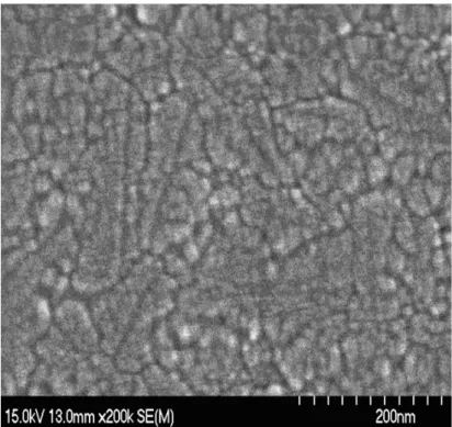
The bird-eye-view scanning electron microscopy (SEM) image of a secco-etched poly-Si film is shown in Fig. 2-2 which apparently reveals a large difference in grain size for Argon-implanted and conventional devices. A better crystalline poly-Si film with larger grain size and lower intragrainular defect is found in the Argon-implanted sample. The possible reasons for the better poly-Si crystallinity for Argon-implanted poly-Si film are as follows: When implanting heavy Argon ions into the a-Si film with the projected range located beyond the a-Si/SiO2
interface which may induce implant-recoiled oxygen atoms from the SiO2 substrate to
accumulate at the interface. The presence of recoiled-oxygen atoms is believed to decrease the interface-nucleation sites of Si grains at the interface. Therefore, when reducing the nucleation sites at the interface of Si/SiO2, the Si atoms will nucleate
from the free top surface of a-Si film. Because the interface Si atoms are bounded to underlying SiO2, the crystallization-generated rearrangement and volume shrink of Si
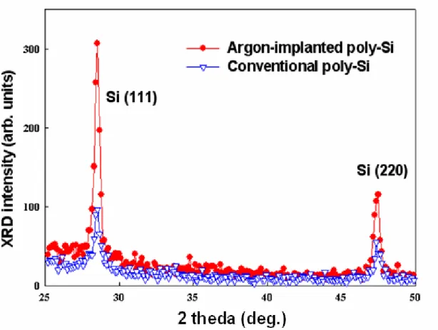
atoms will cause many stress-induced defects in conventional interface-nucleation scheme. However, the crystallization-induced stress can be easily relieved from the surface-nucleation scheme in the Argon-implanted sample. XRD patterns of the poly-Si film for Argon-implanted and conventional samples after SPC annealing are shown in Fig. 2-3. The dominant polycrystalline structure is Si (111) and Si (220) preferred orientation. This result is consistent with that reported by Aoyama et al. [11]. The average grain size can be calculated from the full width at half maximum (FWHM) of the Si (111) peak. The XRD pattern shows that the Argon-implanted sample obviously has sharper and higher XRD intensity in both Si (111) and Si (220) preferred orientation. Therefore, the result further prove that better crystallinity of poly-Si film with larger grain size and fewer intragranular defects can be formed.
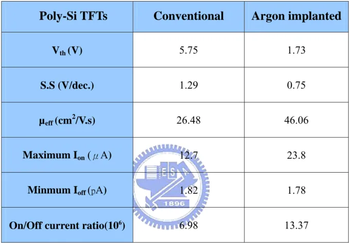
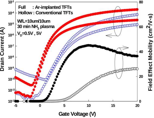
Fig. 2-4 shows the typical transfer characteristics for Argon-implanted and conventional TFTs at drain bias of 0.5V and 5V. The devices have a nominal channel length (L) of 10 um and a channel width (W) of 10 um, respectively. The maximum on-current and minimum off-current are both defined at drain bias of 0.5V. Threshold voltage is defined as the gate voltage required to yield a normalized drain current of IDS = (W/L) × 100 nA at Vd = 0.5V. Distinct improvement in devices
characteristics are acquired for Argon-implanted TFTs. The measured and extracted key devices parameters, including threshold voltage (Vth), subthreshold swing (S.S.), field effect mobility (uFE), maximum on-current, minimum off-current, and on/off
current ratio are summarized in Table 2-1.
Consequently, the performance of Ar-implanted TFTs is significantly improved in Fig. 2-4 The Vth and S.S. of the Ar-implanted TFTs were found to be superior to the conventional ones. It is well-known that the Vth and S.S. are strongly affected by the deep trap states originated from the Si dangling bonds [12]. Because Argon ion is
a noble gas which may not react with Si dangling bonds and contributes any dopant species, the improved performance may not derive from the Argon passivation effect of poly-Si trap states and dopant-.induced lower threshold voltage. Hence, using surface-nucleation SPC by heavy Argon ions implantation can improve the microstructure crystallinity of poly-Si film. Because of the better crystalline poly-Si film, the dangling bonds at the grain boundaries were reduced, effectively.
In addition, the off-state leakage current of the Argon-implanted TFTs was smaller than that of conventional ones. It is well-known that the leakage current was generated from the field-enhanced-emission via trap states near the drain depletion region under a high electric field. The better the crystallinity of poly-Si film, the fewer the trap states can be created. Hence, the leakage current under a high electric field can be reduced. Fig. 2-4 also shows the extracted field effect mobility calculated from the value of transconductance at VDS = 0.5 V. As we can see, the maximum field effect
mobility for the Argon-implanted TFTs is higher than that for the conventional ones. The Argon-implanted TFTs show approximately 70% improvement in field effect mobility. The main cause of the superior device performance for the Argon-implanted TFTs may be further attributed to the fewer Si-Si dangling boonds, and thus better crystalline poly-Si film can be formed.
Fig. 2-5 shows the typical output characteristics (IDS − VDS) at several different
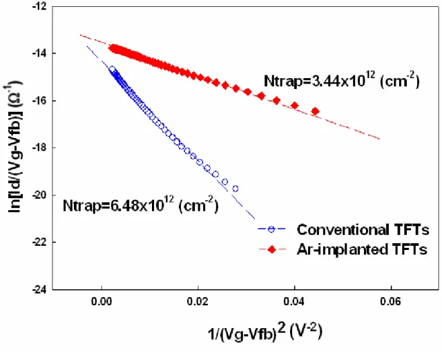
common gate drive for the Argon-implanted and the conventional poly-Si TFTs. As can be seen, the Argon-implanted TFTs exhibit a larger driving current capability than the conventional ones to further confirm that the whole channel region has fewer defect densities and larger silicon grain size in the Argon-implanted poly-Si film. Fig. 2-6 shows the grain boundaries trap state densities (Ntrap) extracted from the slope of
grain-boundary trapping model proposed by Levinson and Proano method [13][14]. It can be found that the Argon-implanted TFT exhibits a Ntrap of about 3.44 × 1012 cm-2,
whereas the conventional one possess a Ntrap of 6.48 × 1012 cm-2. Our results further
verify that Argon-implanted technique has reduced grain boundaries trap states in the poly-Si film due to the larger grain size.
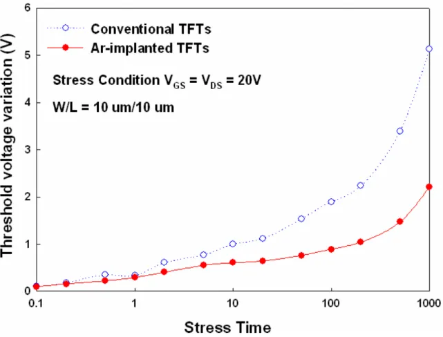
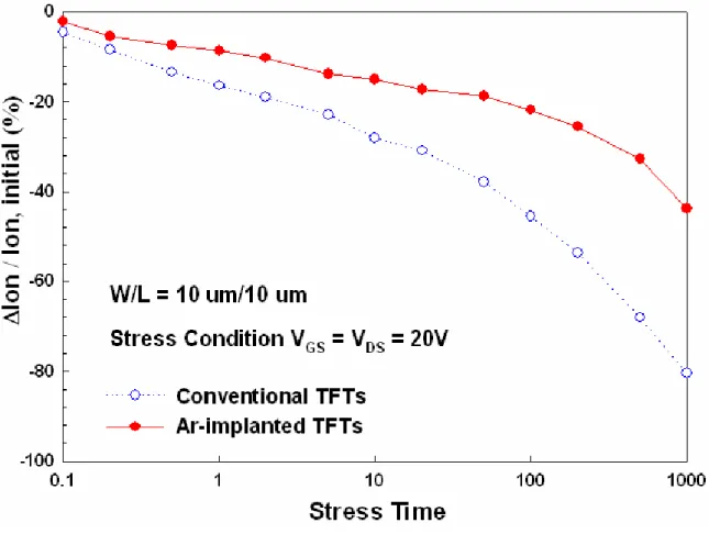
Hot-carrier-stress was performed at VDS = 20V and VGS = 20V for 1000 s to
examine the electrical reliability. The threshold voltage variations and the on-current degradation over hot carrier stress time are shown in Fig. 2-7 and 2-8, respectively. Based on these experimental results, it was clearly observed that the VTH and
on-current have more severe degradation due to the easy broken of Si–Si and Si–H bonds under serious hot carrier stress, causing the larger ∆VTH and ∆ION/ION
degradation in conventional TFTs. In contrast, the Argon-implanted TFTs have higher immunity against the hot carrier stress than conventional TFTs do It is well known that the VTH is strongly dependent on the deep trap states originated from the dangling
bonds at the grain boundaries [12].. The significant enhancement in the electrical reliability can be ascribed to the better microstructure crystallinity of poly-Si film with reduced Si–Si and Si–H bonds at poly-Si grain boundaries in Argon-implanted device.
2.4 Summary
In summary, we have investigated the SPC of a-Si film with reduced nucleation sites created by heavy Argon ions implantation induced-recoiled oxygen rich region at the a-Si/SiO2 interface. It has been found that the interface-nucleation rate was
suppressed, hence the microstructure quality of poly-Si films from fewer nucleation-sites seeded SPC of a-Si at 600oC has been improved. A novel process compatible poly-Si TFTs with Argon-ion implantation is proposed. The field effect
mobility for Argon-ions implanted TFTs is higher than 46.06 cm2/Vs, which was superior to the conventional TFTs. In addition, the Argon-implanted TFTs can possess higher immunity against the hot carrier stress. It is speculated that the larger grain size of poly-Si film will result in fewer grain boundaries defects such as weak Si–Si and Si–H bonds. Fabricating poly-Si TFTs with Argon ions implantation improve not only the electrical performance but also the reliability. Furthermore, the manufacture process is simple and compatible with the conventional poly-Si TFTs fabrication processes.
Reference:
[1] H. Oshima and S. Morozumi, “Future trends for TFT integrated circuits on glass substrates,” in IEDM Tech. Dig., pp. 157–160 1989.
[2] D. Brotherton, “Polycrystalline silicon thin film transistors,” Semicond. Sci.
Technol., pp. 721–738, 1997.
[3] Yoshihiro Morimoto, Yushi Jinno, Kyoko Hirai, Hidenori Ogata, Tutomu Yamada, and Kiyoshi Yoneda, “Influence of the Grain Boundaries and Intragrain Defects on the Performance of Poly-Si Thin Film Transistors,” J. Electrochem. Soc., vol. 144, July 1997.
[4] Eimi Adachi, Takashi Aoyama, Nobutake Konishi, Takaya Suzuki, Yoshiaki Okajima and Kenji Miyata, “TEM Observations of Initial Crystallization States for LPCVD Si Films,” Jpn. J. Appl. Phys., vol. 27, pp. 1809-1811, 1988.
[5] C.-H. Hong, C.-Y. Park, and H.-J. Kim, “Structure and crystallization of low-pressure chemical vapor deposited silicon films using Si2H6 gas,” J. Appl.
Phys., vol. 71, pp. 5427-5432, 1992.
[6] L. Haji, P. Joubert, J. Stoemenos, and N. A. Economou, “Mode of growth and microstructure of polycrystalline silicon obtained by solid-phase crystallization of an amorphous silicon film” J. Appl. Phys., vol. 75, pp. 3944-3952, 1992.
[7] Myung-Kwan Ryu, Seok-Min Hwang, Tae-Hoon Kim, Ki-Bum Kim, and Seok-Hong Min, “The effect of surface nucleation on the evolution of crystalline microstructure during solid phase crystallization of amorphous Si films on SiO2,”
A. Phys. Lett., vol. 71, pp. 3063-3065, 1997.
[8] Myung-Kwan Ryu, Jang-Yeon Kwon, and Ki-Bum Kim, “Solid phase crystallization (SPC) behavior of amorphous Si bilayer films with different concentration of oxygen: Surface vs. Interface-nucleation,” Mat. Res. Mat. Res.
[9] I-W Wu, A Chiang, M Fuse, L. Ovecoglu, and T-Y Huang, “Retardation of nucleation rate for grain size enhancement by deep silicon ion implantation of low-pressure chemical vapor deposited amorphous silicon films,” J. Appl. Phys, vol. 65, pp. 4036-4039, 1989.
[10] E. F. Kenndy, L. Csepregi, J. W. Mayer, and T. W. Sigmon, “Influence of 16O, 12C,
14N, and noble gases on the crystallization of amorphous Si layers,” J. Appl. Phys.
48, 4241, 1977.
[11] T. Aoyama, N. Konishi, T. Suzuki, and K. Miyata, in Materials Research Society
Symposium Proceedings, edited by C. Y. Wang, C. V. Thompson, and K. N. Tu,
“Crystallization of LPCVD Silicon Films by Low Temperature Annealing,” (Materials Research Society, Pittsburgh, PA, 1987), vol. 106, p. 347.
[12] I. W. Wu, T. Y. Huang, W. B. Jackson, A. G. Lewis, and A. Chiang, “Passivation kinetics of two types of defects in polysilicon TFT by plasma hydrogenation,” IEEE
Electron Device Lett., 12, 181, 1991.
[13] J. Levinson, F. R. Shepherd, P. J. Scanlon, W. D. Westwood, G. Este, and M. Rider, “Conductivity behavior in polycrystalline semiconductor thin film transistors,” J. Appl. Phys., vol. 53, pp. 1193–1202, 1982.
[14] R. E. Proano, R. S. Misage, and D. G. Ast, “Development and electrical. properties of intrinsic polycrystalline silicon thin film transistors,”IEEE Trans. Electron Devices, 36, 1915, 1989.
(a) Thermal oxidation grown by furnace
(b) Amorphous Si (a-Si) deposited by LPCVD
Argon ion implantation
(c) Argon ion implantation
Si Wafer
Thermal Oxide
a-Si
Si Wafer
Thermal Oxide
a-Si
Si Wafer
Thermal Oxide
(d) Recrystallization of a-Si film into poly-Si channel by SPC and active region definition
(e) Deposition of TEOS gate oxide by LPCVD and poly-Si gate by LPCVD
Si Wafer
Thermal Oxide
Poly-Si Channel
TEOS Gate Oxide
Poly-Si Gate
Si Wafer
Thermal Oxide
Poly-Si Channel
(f) The gate electrode defined and self-align phosphorous ion implantation (g) Dopant activation
Si Wafer
Thermal Oxide
Poly-Si
n
+n
+n
+Si Wafer
Thermal Oxide
Poly-Si Channel
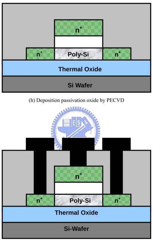
(h) Deposition passivation oxide by PECVD
(i) Contact holes and metal pads formation
Fig. 2-1 Schematic diagram of fabrication process for the Argon implanted poly-Si TFTs
Si-Wafer
Thermal Oxide
Poly-Si
n
+n
+n
+Si Wafer
Thermal Oxide
Poly-Si
n
+n
+n
+Table 2-1 Comparison of device characteristics for the conventional and the Argon implanted poly-Si TFTs.
Poly-Si TFTs
Conventional
Argon implanted
V
th(V)
5.75 1.73
S.S (V/dec.)
1.29 0.75
µ
eff(cm
2/V.s)
26.48 46.06
Maximum I
on(
μA)
12.7 23.8
Minmum I
off(
pA)
1.82 1.78
(a) Argon-implanted poly-Si film
(b) Conventional poly-Si film
Fig. 2-3 XRD patterns of the poly-Si film for the Argon-implanted and the conventional samples after SPC annealing
-5 0 5 10 15 20 10-12 10-11 10-10 10-9 10-8 10-7 10-6 10-5 10-4 10-3 0 20 40 60 80
Dr
ain Cur
rent (A)
Gate Voltage (V)
Field Effect Mobilit
y
(
cm
2
/V-s
)
W/L=10um/10um 30 min NH3 plasma VD=0.5V , 5V Full : Ar-implanted TFTs Hollow : Conventional TFTsFig. 2-4 Transfer characteristics and field effect mobility of the conventional and the Argon implanted poly-Si TFTs with VD = 0.5V , 5V
Fig. 2-5 Output characteristic of the conventional and the Argon implanted poly-Si TFTs
Fig. 2-6 Trap state density extraction of the conventional and the Argon implanted poly-Si TFTs
Chapter 3
High-Performance Poly-Si TFTs Fabricated by
Floating Channel Solid-Phase-Crystallization
Technique
3.1 Introduction
Solid-phase crystallization (SPC) of amorphous silicon (a-Si) is an attractive alternative for polycrystalline silicon (poly-Si) thin-film transistors (TFTs) [1][2]. In application point of view, the electrical characteristics of poly-Si TFTs are strongly correlated to the microstructure of poly-Si film. Among the parameters of microstructure, the grain boundaries and intragranular defects act as scattering centers and midgap traps that are concluded as the determinate factors for the properties of carrier transport [3]. Unfortunately, the traditionally SPC methods obtain an interface-nucleation which has a nucleation of Si atoms begins from bounded a-Si film interface (a-Si/SiO2) and therefore lead to smaller grain size [4]-[6]. Recently, the
surface-nucleation SPC scheme was proposed to improve the microstructure of SPC poly-Si films by initiating the nucleation of Si atoms from the free surface of the a-Si film. Experimental results had been confirmed that those methods will significantly enlarge the grain size and suppress the intragranular defects [7]-[10]. However, those methods are relatively complicated that require additional fabrication procedures and are not practical for TFTs application.
In further simplify the fabrication process, we take the advantage from the SPC scheme proposed by Bo et al. [11] and design the floating channel structure.
According the results concluded from the works of Bo et al., we remove the underlying silicon oxide (SiO2) prior to the SPC. Experimental results confirm that the
grain size and density of intraguanular defects of the floating channel films are greatly improve; moreover, a relatively better electrical property is also obtained. In summarized, we propose and demonstrate a floating channel poly-Si TFT (FC TFT) in this paper that features with simple in process, low cost in fabrication, but superior in performance.
3.2 Experiment
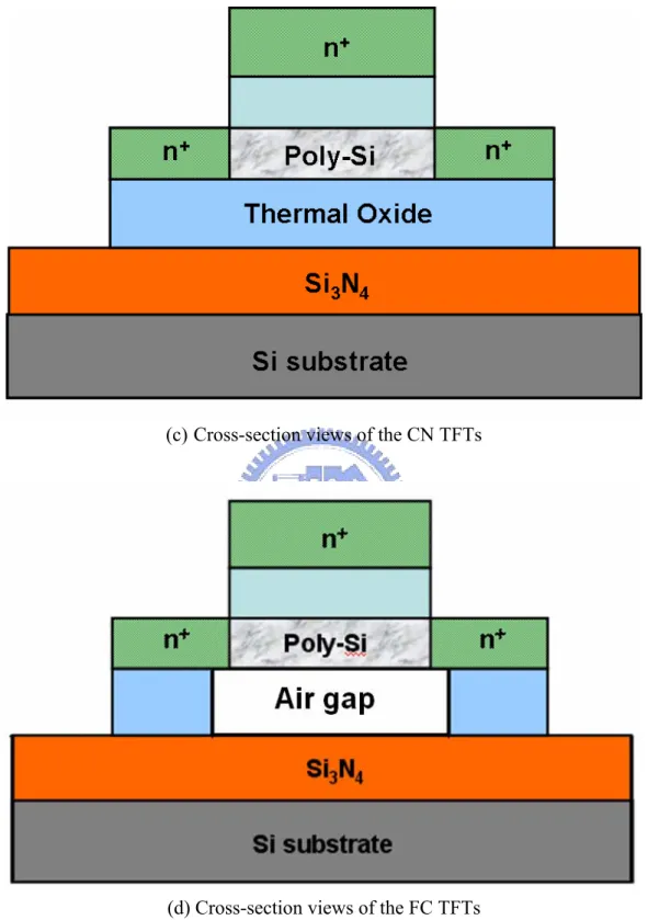
Fig. 3-1 shows the process flow of the proposed poly-Si TFTs. Fig. 3-2(a) is the topological layout of both the conventional TFTs (CN TFTs) and the proposed FC TFTs. Though having the same layout, the cross-section views of the CN and FC TFTs presented in Fig. 3-2(c) and (d) respectively are quite different. The significance could be easily observed that the Si atoms inside channel region are unbounded with the buffer oxide for FC TFTs; on the other hand, the traditional used structure has its channel Si atoms bounded with the buffer oxide. The processes of the FC TFT are exhibited as following: First, silicon nitride, buffered TEOS oxide and undoped amorphous silicon with a thickness of 150nm, 35nm and 50nm were successively deposited by low-pressure chemical vapor deposition (LPCVD) systems at 700℃, 600℃, and 550℃, respectively. Then the amorphous silicon is first patterned into the active channel region. After that, the fluorine-based etchant is performed to remove the buffered oxide underneath the amorphous silicon active channel region. As a result, an air gap was formed to formulate the floating channel shown in Fig. 3-2(b). In comparison, CN TFT structure is also prepared without taking the removing of underneath buffer oxide. The SPC is performed at 600℃ for 24 hours that transfers the amorphous silicon into polycrystalline silicon.
A 100nm TEOS oxide and a 150nm poly-Si were deposited by LPCVD at 600℃ to serve as the gate insulator and the gate electrode. Self-aligned source/drain and gate regions were then done by implantation of phosphors ion at a dose of 5 × 1015 cm-2and a energy of 15 keV. A 400-nm-thick passivation oxide was deposited and then followed with dopant activation at 600℃ for 12 hours. Finally, a NH3 plasma
treatment was performed soon after the definition of contact holes and electrodes at 350℃ for 30 min.
3.3 Results and Discussion
The transmission electron microscope (TEM) image of the FC poly-Si TFTs is shown in the Fig.3-3. This image show that the air gap is under the poly-Si film. The scanning electron microscopy (SEM) images of the Secco etched poly-Si channel film for FC and CN TFT are shown in the Fig. 3-4(a) and (b) respectively. Those images obviously show that a polycrystalline silicon film with larger grain size can be obtained in the suspended structure. The superior grain property could be further investigated from the Fig. 3-5 and Fig. 3-7 that presents both the transfer characteristics and effective density of grain boundary trap states for the FC and CN devices. It could be concluded from transfer curves that the FC TFT has smaller subthreshold swing (S.S.), higher on/off ratio and better driving capability than the CN TFT does. Furthermore, based on the grain-boundary trapping model developed by Levinson and Seki et al. [12][13], the slope of ln [IDS/(VGS-VFB)] versus
1/(VGS-VFB)2indicates the effective density of grain boundary trap states (Ntrap) of the
FC TFT is about four times smaller than that of the CN one. The consequence further verifies that the FC TFTs have much fewer grain boundaries defects owing to its relatively larger grains. In more precisely comparing the difference between the CN
and FC TFTs, key device parameters are calculated, summarized and listed in Table 3-1. Among those parameters, the on/off current ratio is the ratio of the maximum on state current to the minimum off state current for drain bias at 3 V. Threshold voltage is defined as the gate voltage to yield a normalized drain current Id/ (W/L) equal to
10-7 A at Vd = 0.5 V. Table 3-1 summarizes that the Vth is significantly reduced from 6
to 1.62 V; this highly correlated to the S.S. that is decreased from 0.971 to 0.264 V/dec. Moreover, the improvement of the S.S. is owing to the fact that the trap state density in FC device is only quarter of the CN ones. Similar with the S.S., the reduction of the trap density leads the field effect mobility (uFE) three times
enlargement and the on/off current ratio almost one order in advance. Those results are highly corresponding to the SPC mechanism in changing amorphous silicon into polycrystalline silicon. For the fact that both the interface rearrangement and volume contraction are dominant for the crystallization of silicon atoms, the tensile stress will be induced during the process. Accordingly, strong bounding between silicon atoms to the underlying SiO2 for conventional method will certainly produce a lot of crystalline
defects (microtwins, dislocation, etc.) to relief the stress. Under such condition, a large number of nucleation sites could be formed and lead to smaller silicon grains. Nevertheless, in the case of floating channel, the removing of underlying SiO2 makes
the silicon atoms barely bound to the underlying SiO2. It is nearly free from the
nucleation associated to the interface of Si/SiO2. As a result, the crystallization
correlated stress generation can be easily relieved with featuring fewer nucleation sites; in addition, make a polycrystalline silicon with lower defect density and larger silicon grains are created. Fig. 3-6 shows the output characteristics (ID-VD) for FC and
CN TFTs. The FC TFTs exhibits a larger driving current capability than CN ones.
This confirms that the floating channel polycrystalline silicon film has lower defect density over whole channel region.
3.4 Summary
We have proposed a high-performance polycrystalline silicon TFTs with larger grain size and lower intragranular defects by a simple floating channel solid-phase crystallization technique. The FC TFTs not only exhibit improved turn-on characteristics but also keep the low off-state leakage current by successfully improving the microstructure of floating polycrystalline silicon films. Superior effective grain-boundary trap density and field effective mobility further confirm that good crystallinity and larger grain size of polycrystalline silicon film are fabricated by this method. Consequently, the proposed FC TFT is potentially suitable for future high-performance large-area device applications.
Reference:
[1] H. Oshima and S. Morozumi, “Future trends for TFT integrated circuits on glass substrates,” in IEDM Tech. Dig., pp. 157–160, 1989.
[2] D. Brotherton, “Polycrystalline silicon thin film transistors,” Semicond. Sci.
Technol., pp. 721–738, 1997.
[3] Yoshihiro Morimoto, Yushi Jinno, Kyoko Hirai, Hidenori Ogata, Tutomu Yamada, and Kiyoshi Yoneda, “Influence of the Grain Boundaries and Intragrain Defects on the Performance of Poly-Si Thin Film Transistors,” J. Electrochem. Soc., vol. 144, July 1997.
[4] Eimi Adachi, Takashi Aoyama, Nobutake Konishi, Takaya Suzuki, Yoshiaki Okajima and Kenji Miyata, “TEM Observations of Initial Crystallization States for LPCVD Si Films,” Jpn. J. Appl. Phys., vol. 27, pp. 1809-1811, 1988.
[5] C.-H. Hong, C.-Y. Park, and H.-J. Kim, “Structure and crystallization of low-pressure chemical vapor deposited silicon films using Si2H6 gas,” J. Appl.
Phys., vol. 71, pp. 5427-5432, 1992.
[6] L. Haji, P. Joubert, J. Stoemenos, and N. A. Economou, “Mode of growth and microstructure of polycrystalline silicon obtained by solid-phase crystallization of an amorphous silicon film” J. Appl. Phys., vol. 75, pp. 3944-3952, 1992.
[7] I-W Wu, A Chiang, M Fuse, L. Ovecoglu, and T-Y Huang, “Retardation of nucleation rate for grain size enhancement by deep silicon ion implantation of low-pressure chemical vapor deposited amorphous silicon films,” J. Appl. Phys, vol. 65, pp. 4036-4039, 1989.
[8] Myung-Kwan Ryu, Seok-Min Hwang, Tae-Hoon Kim, Ki-Bum Kim, and Seok-Hong Min, “The effect of surface nucleation on the evolution of crystalline microstructure during solid phase crystallization of amorphous Si films on SiO2,”
[9] Myung-Kwan Ryu, Jang-Yeon Kwon, and Ki-Bum Kim, “Solid phase crystallization (SPC) behavior of amorphous Si bilayer films with different concentration of oxygen: Surface vs. Interface-nucleation,” Mat. Res. Mat. Res.
Soc. Symp. Proc., vol. 621, pp. Q6.3.1- Q6.3.6, 2000.
[10] Tae-Hoon Kim, Myung-Kwan Ryu, and Ki-Bum Kim, “A comparison of the kinetics and the evolution of microstructure of the solid phase crystallized a-(Si0.7Ge0.3/Si) and a-(Si/ Si0.7Ge0.3) bilayer films; Interface versus surface
nucleated films,” Jpn. J. Appl. Phys., vol. 37, pp. 108-111, 1998.
[11] Xiang-Zheng Bo, Nan Yao, Sean R. Shieh , Thomas S. Duffy, and J. C. Sturm, “Large-grain polycrystalline silicon films with low intragranular defect density by low-temperature solid-phase crystallization without underlying oxide,” J.
Appl. Phys., vol. 91, pp. 2910-2915, 2002.
[12] J. Levinson, F. R. Shepherd, P. J. Scanlon, W. D. Westwood, G. Este, and M. Rider, “Conductivity behavior in polycrystalline semiconductor thin film transistors,” J. Appl. Phys., vol. 53, pp. 1193–1202, 1982.
[13] S. Seki, O. Kogure, and B. Tsujiyama, “A semi-empirical model for the field-effect mobility of hydrogenated polycrystalline-silicon MOSFET’s,” IEEE
Trans. Electron Devices, vol. 35, pp. 669–674, 1988.
(a) Topological layout of both the CN TFTs and the proposed FC TFTs
(c) Cross-section views of the CN TFTs
(d) Cross-section views of the FC TFTs
Fig. 3-2 Topological layout , 3-D structure and Cross-section views of the CN TFTs and the proposed FC TFTs
Table 3-1 Comparison of device characteristics for the CN and the FC poly-Si TFTs.
Poly-Si TFTs
CN TFTs
FC TFTs
V
th(V)
6.0 1.62
S.S (V/dec.)
0.971 0.264
µ
eff(cm
2/V.s)
21.06 66.87
N
trap(cm
-2)
1.36 × 10
127.1
× 10
11(a) FC poly-Si film
(b) CN poly-Si film
Fig. 3-5 Transfer characteristics and field effect mobility of the conventional and the floating channel poly-Si TFTs with VD = 0.5V , 3V