A
Novel
Top
Emission Pixel Circuit Compensating
for
TFT
Threshold
Voltage Variation and Luminance
Degradation
of OLED
Chih-Lung Lin*,
Kuo-Chao Liao
Abstract-This work demonstrates a novel pixel circuit bottom emission [3]. However, the aperture ratio of the pixel composed of top emission architecture with a voltage circuit with top emission architecture can be significantly programming method. Besides compensating for the increased [6].
threshold voltage variation of TFTs, the proposed circuit During recent years, the degradation and lifetime of OLED can improve the luminance degradation of active-matrix are the main concerns. With long term operation, luminance organic light-emitting diode (AMOLED) by using OLED and efficiency of OLED often decay gradually. Thus,
voltage as a feedback of OLED luminance degradation. In numerouscompensation schemesareproposedtopostponethe addition, the reversed-bias voltage applied to OLED can degradation of OLED[4], [5], [7], [8]; theseapproachescanbe suppress the degradation of OLED. The simulation results categorized as optical-feedback compensation [7], and circuit
showthat the proposed circuit can effectively compensate compensation [4], [5], [8]. Although optical-feedback scheme for TFT threshold voltage variation and improve can compensate for OLED luminance degradation, the luminancedegradation of OLED. compensation efficiency is sensitivetoambientlight [4]. Shieh
etal. proposedan acdriving method to prolong the lifetime of
OLEDs by using the reversed-bias voltage [8]. However, AVTH Index Terms-Active-matrix organic light-emitting is not compensated and the display doesn't perform well diode (AMOLED), reversed-bias voltage, top mission, against non-uniformity. Lee etal. proposed a novel pixel circuit
degradation with the stable current independent of AVTH of TFTs and
OLED,but luminance still drops due to OLED degradation [5]. Forthe purpose of holding the same luminance, our previous
I.
INTRODUCTION
research proposed the OLED current can be compensated by aOrganic light-emitting diode(OLED) displays have attractive feedback of OLED voltage [4]. OLED degradation can be
attributes,suchaswide viewangle, highcontrastratio, and fast effectively improved, but overmuch TFTs affect the aperture
response time [1]. However, process variation in electrical ratio and luminance efficiency.
characteristics of low-temperature polycrystalline-silicon The proposedpixel circuit with topemission architecture can
(LTPS) or hydrogenated amorphous silicon (a-Si:H), such as
significantly
improve the aperture ratio. Meanwhile, thethreshold voltage (VTH), causes differences in the OLED reversed bias voltage can suppress the degradation ofOLED
currentamongpixelsand the display is non-uniformity. Thus, and the luminance can be improved by the feedback various compensation circuits have been published and compensation of OLED voltage [8]. Therefore,thedisplay has
generally classified bythecurrent
[1]
andvoltage programming better uniform luminance and a high degree of immunity tomethods [1]-[5]. Althoughthe current method can compensate
AVTH
for AMOLEDdisplay. The simulation results show that for the thresholdvoltagevariation(AVTH),the constant current the proposed circuit can compensate forAVTH
and improvethesource is difficult to design for controlling the small current luminance by OLED voltage compensation. level and the charging time is prolonged for low data current
[2].The voltage programming method can effectively II. PROPOSED PIXEL CIRCUIT OPERATION
compensate for TFTthreshold voltage variation. Besides, the Fig. I shows the equivalent circuit of the proposed circuit and aperture ratio is a critical issue for AMOLED applications. driving signals. The proposed pixel is composed of a driving FewerTFTscanimprove aperture ratio in a pixel circuit with TFT
(TI),
four switching TFTs (T2-T5), two storage capacitors (C1-C2) and an OLED, three scan lines(VSCAN1-VSCAN3), a data line (VDATA) and PVDD is a power supply line. VREF is a The authors are with the Department of Electrical Engineering, constant voltage source line and set to 3V. The scan linesNational Cheng Kung University, Tainan, 701-01, Taiwan, Republic (VSCAN1_VSCAN3) range is between -20-20V. PVDD, Vp and of China (e-mail: c1iami~cueut). VSS are set to -2 3V, -6V and -9V, respectively. A\VDATA range is about between-6.5--4V. C1 and C2are 0.3pf. VOLED
is the applied voltage when thecurrent passesthroughOLED.
PVDD
TheOLED current canbe analyzed by thegate-sourcevoltage ofTI.T2is used for the diode connection of TI. VSCAN1-VSCAN3
are used to control TFTs (T2-T5) individually. VREF is a
VSCAN2 VSCAN3
reversed-biasvoltage usedtoextend the lifetime of OLED. The
frame ofa
pixel
is as showed inFig.
1(b),
and theoperation
REFscheme and compensation principle of the proposed pixel
V
T3T4
circuitaredescribedasfollows.
1) ResetPeriod: During this period, T2, T3,T4andT5 are
TlICTl
allonand TI is in diode connection. Thevoltages of node l
NI,N2,and N4 are
allVREF,
thevoltageof node N3 is Vp-andPVDDis low. At thistime,VNIislarger thanPVDD
and the reversed-biasvoltage canaccelerate therecoveryof _
OLEDdegradation. Thevoltagesofnodes, VNI,VN2, VN3 T
and VN4atthisperiodare
VSCA
_T5
VNI =VN2=VN4 VREF
VN3 = (i)
VPATA
2) Programming Threshold Voltage Period: During the (a)
second
period,
T4 and OLEDareoff. BecauseofTI in ) ) (3 f)()diode
connection,
Ci starts to discharge throughTi until (1) ( (3 ( (thegatevoltageofTI (VN4)iS VSS+VTH TFTI (thethreshold
voltage
ofTI).
Thevoltages
ofnodes,
VN1,
VN2, VN3 and _..._... 3VN4atthisperiodare
PVDD
V4 o 4#i 4'.4.4. 20V
NI N2 N4 TH_TFT1
VN3
VP
(2) VCAI.2... .
X..-.*20V
3)
DataInput
Period: T2is off. At thebeginning,
because .-j20VVN3 is
changed
fromVp
toVP+AVDATA,
VN4ischanged
_... ...from
VSS+VTH_TFTI
toVSS+VTH_TFTi+AVDATA.
Meanwhile,
V.AtVP
PVDDisturned
high
and thecurrentbegins
topassthrough
AOLEDand TI. Therefore, VNI and VN2areboth
PVDD-VOLED. Thevoltageof each nodeatthisperiodis (b)
VNI
=VN2 =PVDD-VOLED
Fig.i.
(a) Equivalent circuit of the proposed pixel circuit. (b)VN3=VP+
AVDATA
Driving signals.
(i)
ResetPeriod,
(2)
Programming
ThresholdVN4
=VSS+VTH
TFTI+AVDATA
(3)
VoltagePeriod,(3) DataInputPeriod(4)HoldingVOLED Period,and
(5)
Emission Period.4) HoldingVOLEDPeriod: Thevoltagesof CI and C2are
Therefore,
the OLED current(ILED)
can be determinedby
N4-N3 and
N3-N2,
respectively,
thegate-sourcevoltage ofTI.
IOLEDiSVCl
V ~~VVN4 -VN3 VSS
-v ~v +AV+VTH
TFTI-PVDD+VoLEDVP
~~OLEDI2kT
k1(VGS V2
VC2
VN3 VN2 VP
+AVDATA
-PVDD+VOLED
(4) )=-kl
(VN4
-VSSVTH
TFTIwhere
Vc,
andVc2arethe differentvoltagesstored inCI 2andC2,individually. -
k,
(VSS +VTH
T_T
+AVDATA
5) Emission Period: During emission period, T4 is turned - PVDD + VOLED + VREF VSS
2VTH_TFT1
on and VN2 is changed from PVDD-VOLED toVREF. i
Therefore, VN4 iS boosted from VSS±VTH_TFT1±AVDATA to =-k(AVDATA -PVDD +VO +VRF(5
VSS±VTH_TFT1±AVDATA± VJHJFPVDD±VOLED
due to the 2OE E 5charge conservation of
Cil
and C2.where k1 is COXW1/L1. 386
Besides, PVDD and VREF are both 3V. Therefore, the 1100
equation (5) can be simplified as follows. 1000 = PfoposedPixelCiraLtwithV aHOV
---+e ProposedPixel CircLtwith LViia +O03V 1;
900 ConventionalPixelCirctcwithAV -3V / ConventionalPixelCircutwithAV H=OV
IOLLD
=-kl(VOLLD + 0\ VI)ATA ) (6) 800 + Co nveConventionalPixeCircitwithAxVH=+0.3V
~~~~~~~2
X 00JIOLED
2_+AVDATAT (6) 700600 0
From equation (6), IOLED is independent of AVTH and only J affectedbyVOLED+AVDATA.Consequently,AVTHdoesn't affect O 400
the OLED current. Moreover, VOLED canprovide another part 300
-of the OLED current andimprove the display luminance due to 200 .
OLED degradation. In the first period of one frame, Reset 100_
Period, the reversed-bias voltagecanaccelerate the recovery of 0 I
OLEDdegradationand extend the OLED lifetime. -6.5 -6 Inp1ut-5.5DataVoltage-5 (V) -4.5 -4
Fig. 3. Simulation of OLED current with threshold voltage
III. SIMULATION
RESULTS variation betweeninputdata range. Toconfirm thefunctionality of theproposed pixel circuit,the - X/5hAsimulation results are achieved by AIM-SPICE. Simulation
l4
nAmodel parameters were extracted from the measurements of 9rn fabricated OLED
panels.
TheVTH
ofn-type
TFTis 1.88V andthe width andlength of TI are 12pm and 25ptm,respectively. -The width andlength of T2, T3, T4 and T5 are all 5,um. The
600X
thresholdvoltagevariation ofTFTisset to±0.3V.Fig. 2 shows the gate voltage of TI with AVTH during one frame operation. The simulation result represents that the
voltage stored in Cl includes AVTH information and the
t0
uniformity of OLEDcurrent canbe achieved. 20
Fig.
3 shows the simulation of OLED current with AVTH I 46. . ~~~~~~~~~~~~~~~00.t 0.2 Us 0A 0.5
between
input
data range.Compared
with that of the V Si(s
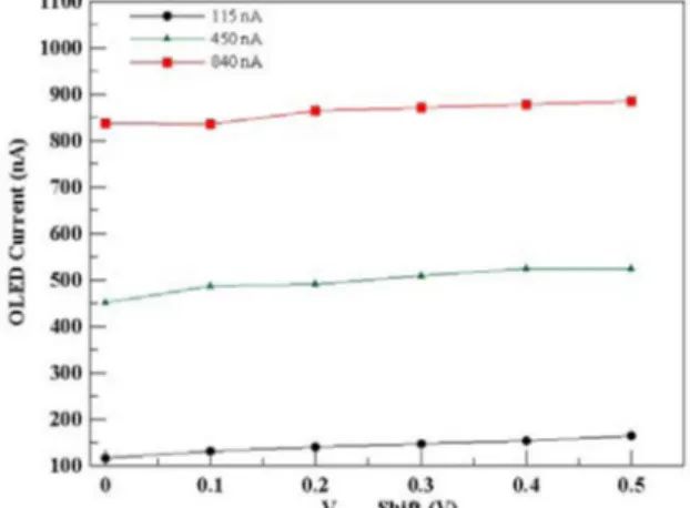
conventional 2T1Cpixelcircuit,OLEDcurrentoftheproposed Fig. 4. OLED current as a function of shift in OLED voltage.
pixelcircuit areobviouslyindependentof AVTH.Therefore, the
result illustrates that the proposed pixel circuit successfully iv. CONCLUSION
compensate for AVTH and has superior immunity against Inthis
study,
anoveltop emission architecturepixel
circuitnon-uniformity.
with five TFTs and two capacitors is presented. Inaddition toFig.4shows the result of OLED current with VOLED shift. As
compensating
for the thresholdvoltage variation,
theproposed
VOLEDincreases,OLED currentcanbecompensatedtoimprove pixel circuit can increase the aperture ratio and suppress the the
degradation
of OLED.degradation
of OLED byreversed-bias
voltageapplications.
5.0 OLED luminance canbe
partially
compensated by
afeedbackvoltage of VOLED in OLED current. Therefore, this proposed
| . . .. [
vl~1SS3v
1 | pixelcircuit can improve uniformity and the lifetimeof
OLED-0.0 Gate\ I[tageofT1 |TH=LSSV displays.
// \~~~~~~%TH=1lS-0O3V
-X.0 v ACKONWLEDGMENT
The authors would liketothank AU
Optronics
Corporation,
Hsinchu, Taiwan, R.O.C., for its technical support and the
-o.ol,
X | National Science Council oftheRepublicofChina,Taiwan,
for______________________________________ _ , lfinancially supporting this research under Contract No. NSC
(2)1 (3)Eli} (5) 96-2221-E-006-131-MY3.
0O*u $5OOu 100Ou0 15OOiu 200Ou0
Tiiiw (seL REFERENCES
Fig. 2. The simulation of the gate voltage of the driving TFT
(Ti) with threshold voltage variation. (1) Reset Period, (2) [1] R. Dawson, Z. Shen, D. A. Furest, S. Connor, J. Hsu, M. G. Programming ThresholdVoltage Period, (3) Data Input Period Kane, R.G. Stewart, A. Ipri, C. N. King, P. J. Green, R. T. (4) Holding VOLED Period, and (5) Emission Period. Flegal, S. Pearson, W. A. Tang, S. Van Slyke, F. Chen, J.
Shi,M. H. Lu,andJ.C. Sturm,"Theimpact of the transient
response oforganic light emitting diodes onthe design of active matrix OLED displays," in IEEE IEDMMeeting,
1998, pp. 875-878.
[2] S. H. Jung, W. J. Nam, and M. K. Han, "A new
voltage-modulated AMOLED pixel design compensating for threshold voltage variation in poly-Si TFTs," IEEE
Electron Device Lett., vol. 25, no. 10, pp. 690-692, Oct.
2004.
[3] C. L.LinandT. T.Tsai, "Anovelvoltage drivingmethod using 3-TFT pixel circuit for AMOLED," IEEEElectron
Device Lett., vol. 28,no.6,pp.489-491,Jun.2007. [4] C.L.LinandY. C.Chen,"Anovel LTPS-TFTpixelcircuit
compensating for TFT threshold-voltage shift and OLED
degradation for AMOLED," IEEE Electron Device Lett., vol. 28,no.2,pp. 129-131,Feb. 2007.
[5] J. H. Lee, J.H. Kim, andM. K. Han, "A new a-Si:HTFT
pixel circuit compensating the threshold voltage shift of a-Si:H TFT and OLED for active matrix OLED," IEEE
Electron Device Lett., vol. 26, no. 12, pp. 897-899, Dec.
2005.
[6] M.-H. Lu, M. S. Weaver, T. X. Zhou, M. Rothman, R. C.
Kwong, M. Hack, and J. J. Brown, "High-efficiency
top-emitting organic light-emitting devices," Appl. Phys. Lett.,vol. 81,pp.3921-3923, 2002.
[7] D. Fish, N. Young, S. Deane, A. Steer, D. George, A.
Giraldo, H. Lifka, 0. Gielkens, and W. Oepts, "Optical
feedback for AMOLEDdisplay compensation using LTPS and a-Si:Htechnologies,"inProc. SIDTech. Dig., 2005,pp.
1340-1343.
[8] Y. C. LinandH. P. D. Shieh, "Improvement ofbrightness
uniformity byAC drivingscheme for AMOLED display,"
IEEEElectron DeviceLett., vol. 25, no. 11, pp. 728-730,
Nov.2004.