Realization of In 2 O 3 thin film transistors through reactive evaporation process
Dhananjay and Chih-Wei Chu
Citation: Applied Physics Letters 91, 132111 (2007); doi: 10.1063/1.2789788
View online: http://dx.doi.org/10.1063/1.2789788
View Table of Contents: http://scitation.aip.org/content/aip/journal/apl/91/13?ver=pdfcov Published by the AIP Publishing
Articles you may be interested in
Low-voltage ZnO thin-film transistors based on Y 2 O 3 and Al 2 O 3 high- k dielectrics deposited by spray pyrolysis in air
Appl. Phys. Lett. 98, 123503 (2011); 10.1063/1.3568893
Physical and optical properties of room temperature microwave plasma anodically grown Ti O 2 J. Vac. Sci. Technol. A 27, 725 (2009); 10.1116/1.3154514
Interface dependent electrical properties of amorphous In Ga Zn O 4 thin film transistors J. Vac. Sci. Technol. B 27, 126 (2009); 10.1116/1.3058717
Ambipolar transport behavior in In 2 O 3 /pentacene hybrid heterostructure and their complementary circuits Appl. Phys. Lett. 93, 033306 (2008); 10.1063/1.2949872
High-mobility thin-film transistor with amorphous In Ga Zn O 4 channel fabricated by room temperature rf-magnetron sputtering
Appl. Phys. Lett. 89, 112123 (2006); 10.1063/1.2353811
This article is copyrighted as indicated in the article. Reuse of AIP content is subject to the terms at: http://scitation.aip.org/termsconditions. Downloaded to IP: 140.113.38.11 On: Thu, 01 May 2014 00:07:20
Realization of In
2O
3thin film transistors through reactive evaporation
process
Dhananjay
Research Center for Applied Sciences, Academia Sinica, Taipei, Taiwan 11529, Taiwan
Chih-Wei Chua兲
Research Center for Applied Sciences, Academia Sinica, Taipei, Taiwan 11529, Taiwan and Department of Photonics, National Chiao-Tung University, Hsinchu 30013, Taiwan
共Received 11 July 2007; accepted 5 September 2007; published online 27 September 2007兲 In2O3 thin films have been grown by reactive evaporation of indium in ambient oxygen. The films were structurally characterized by x-ray diffraction共XRD兲 and atomic force microscopy techniques. The results of XRD revealed that the films were polycrystalline in nature with preferred 共222兲 orientation. The as-grown films were subjected to various annealing treatments to modulate the conductivity of the films for thin film transistors 共TFTs兲. TFTs fabricated on SiO2 gate dielectric
exhibited an on/off ratio of 104 and a field-effect mobility of 27 cm2/ V s. High on-state current
makes them potential candidates for flat-panel display devices. © 2007 American Institute of
Physics. 关DOI:10.1063/1.2789788兴
Indium oxide 共In2O3兲 is a n-type oxide semiconductor
with a wide band gap共⬃3.6兲 at room temperature. Thin films of In2O3are superior to other transparent oxide counterparts such as ZnO, CdO, and SnO2, largely due to their high
mo-bility of 10– 75 cm2V−1s−1 at a carrier density of
⬃1019– 1020cm−3.1
It belongs to a complex cubic bixbyte structure with a lattice parameter a = 10.11 Å.2 The coexist-ence of high optical transmittance in the visible region and high electrical conductivity makes them potential candidate as active layers in thin film solar cells.3Moreover, the elec-trical property of this material could easily be controlled by simple heat treatments.4 Such a heat treatment changes the composition of the film due to the annihilation of the oxygen vacancy, thereby leading to stoichiometric films.
Due to the large mobility and low processing tempera-tures, transparent amorphous oxide semiconductors have re-ceived much attention in the current research field of thin film transistors. Combinatorial approach5 has been utilized by the earlier researchers to find a suitable material for the active channel layer, for example, In–Ga–Zn–O,6In–Zn–O,7 Zn–Sn–O,8 and In–Sn–O.9 However, the different vapor pressures of the individual element lead to the difficulty in tuning the optimum composition and the reproducibility. Hence, finding a best composition becomes difficult in such a multicomponent systems. According to the earlier research-ers, such a multicomponent system was necessary to reduce the electron background concentration and to enhance the channel resistivity. For example, to suppress the channel con-ductivity in In2O3, divalent Zn partially replaces In, i.e.,
90 wt % In2O3– 10 wt % ZnO and were reported in the
literature.10 Moreover, most of these multicomponent oxide TFTs reported in the literature were amorphous in nature. Perhaps it will be more interesting if undoped In2O3could be
used as a channel layer in its crystalline form. So the moti-vation of the present work is to utilize In2O3 as a channel
layer in its undoped form. In the present article, we demon-strate the fabrication of undoped In2O3 thin film transistors
without any external doping. This was feasible with a simple thermal evaporation technique in high purity oxygen ambient and the subsequent annealing treatments. In2O3thin films are shown to be promising candidates as channel material with high mobility for the TFTs.
The cross-sectional view of the device structure used in the present work is presented in Fig.1. Bottom gate TFTs were fabricated on heavily doped n-type silicon substrates with 300 nm of thermally oxidized silicon dioxide. A 20 nm In2O3 thin film was then deposited on SiO2 gate dielectric
through thermal evaporation process. Prior to the deposition, the chamber was pumped down to⬃10−6Torr. Indium and
oxygen of high purity were used as evaporation source and reactive gas, respectively. The flow rate of the gas was con-trolled by means of a mass flow controller. Subsequently, deposition was carried out at a partial pressure of ⬃2 ⫻10−4Torr. The substrate temperature was fixed at 100 ° C.
The deposition rate共0.2 Å/s兲 and thickness 共⬃20 nm兲 of the film were in situ monitored by means of quartz crystal moni-tor. The as-deposited films had a sheet resistance of 50 k⍀. The films were subjected to air annealing in the temperature range of 200– 300 ° C for 2 h to modulate the conductivity. Finally, silver source and drain electrodes were deposited onto the In2O3channel layer by thermal evaporation through
a兲Author to whom correspondence should be addressed. Electronic mail:
[email protected] FIG. 1. 共Color online兲 Schematic diagram of the In2O3thin film transistor.
APPLIED PHYSICS LETTERS 91, 132111共2007兲
0003-6951/2007/91共13兲/132111/3/$23.00 91, 132111-1 © 2007 American Institute of Physics
This article is copyrighted as indicated in the article. Reuse of AIP content is subject to the terms at: http://scitation.aip.org/termsconditions. Downloaded to IP: 140.113.38.11 On: Thu, 01 May 2014 00:07:20
a mechanical shadow mask. The typical channel length and width were 100 and 2000m, respectively. To ensure better source and drain contacts on the In2O3active channel layers, air annealing of the device was carried out at 200 ° C for 15 min. The structure details of the In2O3 thin films were
determined by x-ray diffraction using Cu K␣ radiation. Atomic force microscopy was used to get an insight into the surface morphology and roughness of the films. A semiquan-titative analysis of the film composition was carried out us-ing energy-dispersive analysis of x rays. Electrical character-ization of the film was carried out using an HP 4156 semiconductor parameter analyzer. Device testing was real-ized in a glovebox under N2environment.
Figure 2 shows the x-ray diffraction 共XRD兲 pattern of the In2O3 thin films annealed at two different temperatures,
namely, 200 and 300 ° C for 2 h. The semitransparent as-deposited films were found to be amorphous in nature and hence, not displayed in Fig. 2. The air annealing of the samples at 200 and 300 ° C induces crystallinity in the films and the films exhibited the preferred共222兲 orientation, con-firming bixbyite structure.11The full width at half maximum 共FWHM兲 of 共222兲 diffraction peak was 0.48° and 0.32° for the films annealed at 200 and 300 ° C, respectively. Such a small FWHM ensures the high quality of the films. More-over, the composition of the films was measured using the energy dispersive analysis of x rays and it was found that the ratio of O / In is well above the stoichiometric value 共=1.5兲 共Ref.12兲 for In2O3, indicating excess of oxygen in the films.
Such a composition共In=27 and O=73 at. %兲 was desirable for getting the proper channel resistivity for the TFTs.
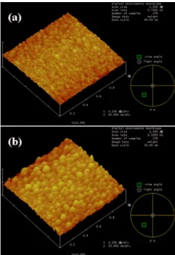
Atomic force microscopy 共AFM兲 image of the In2O3 thin films that were annealed at 200 and 300 ° C for the TFT fabrication are displayed in Figs.3共a兲and3共b兲, respectively. To compare the smoothness of the films annealed at different temperatures, their root-mean-square 共rms兲 roughness was analyzed. The films were atomically smooth and dense grain morphology was observed. The surface roughness plays a major role in the device performance and it has been reported
in the literature.13 It has been found that the active channels with minimal surface roughness leads to better device performance.14,15 The rms roughness of the films derived from AFM was around 1.4 and 4.2 nm for the films annealed at 200 and 300 ° C, respectively. It was found that the thin film transistors fabricated with In2O3 thin films grown at
300 ° C exhibited a large leakage current and hence poor on/off ratio共data not shown兲 compared to the films grown at 200 ° C. This is mainly due to the higher surface roughness of the samples grown at 300 ° C compared to the films grown at 200 ° C and earlier researchers have observed such a phe-nomena previously.14The rms roughness and the relative in-tensity of the共222兲 peak 共Fig.2兲 have shown a similar
varia-tion with annealing temperature and such phenomena were observed in Sn doped In2O3 systems by the earlier
researchers..16 Hence, the surface roughness plays a major role in the performance of the device and the annealing tem-perature of 200 ° C was found to be optimal for the better performance of the device. Moreover, increase in grain size with increase in annealing temperature was observed. In other words, there was a decrease in the grain boundary den-sity due to the agglomeration of the grains, which leads to decrease in grain boundary scattering of the carriers. This, in turn, results in increase in the conductivity. Hence, the over-all carrier concentration of the films increases drasticover-ally with the increased grain size and the channel becomes too conductive, thereby resulting in a poor on/off ratio and a large leakage current of the device. Hence, from the AFM investigations, it infers that air-annealing temperature of 200 ° C is desirable for the In2O3thin films for getting better performance of the device.
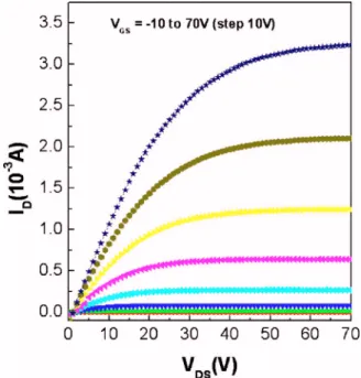
Figure 4 shows the representative drain-source current 共ID兲 as a function of drain to source voltage 共VDS兲 at various
gate voltages of the In2O3 based TFTs with SiO2 gate
insu-lators. Typical channel width共W兲 to length 共L兲 ratio used in the present study, i.e., W / L was 20. The ID-VDS curve
indi-cates that the drain current increases with increase in gate FIG. 2. 共Color online兲 X-ray diffraction pattern of the In2O3 thin films
annealed at different temperatures. FIG. 3.共Color online兲 AFM images of the In2O3thin films annealed for 2 h
at共a兲 200 °C and 共b兲 300 °C.
132111-2 Dhananjay and C.-W. Chu Appl. Phys. Lett. 91, 132111共2007兲
This article is copyrighted as indicated in the article. Reuse of AIP content is subject to the terms at: http://scitation.aip.org/termsconditions. Downloaded to IP: 140.113.38.11 On: Thu, 01 May 2014 00:07:20
voltage, exhibiting the apparent field effect. The transistor operates in n-type depletion mode and exhibits a well-defined pinch-off and saturation region. The channel resistiv-ity of⬃10 ⍀ cm was calculated from the linear slope of the output characteristics at zero gate voltage. Similar to most of the inorganic oxide TFTs, such as ZnO,17 the fabricated In2O3 TFTs obey the standard field-effect transistor theory,
with the Fermi level in the channel fully modulated by the gate and the drain voltages. Moreover, the device had a high output current of the order of milliamperes, which makes it a promising candidate for devices such as smart cards, electric motors and light emitting diodes.
Figure5shows the variation of IDSas a function of VGS
at a fixed drain voltage. The typical on/off ratio of 104 was
estimated. The threshold voltage and field-effect mobility in the saturated regime were estimated using the following re-lation:
ID=
WCiFE
2L 共VGS− VT兲
2, 共1兲
where Ciis the capacitance per unit area of the gate
dielec-tric, VT is the threshold voltage, and FE is the field-effect
mobility. The threshold voltage and the field effect mobility computed from the x-axis intercept of the square root of ID
versus VGS plot and the slope of the plot were found to be
10.5 V and 27 cm2/ V / s, respectively. The obtained value of
mobility was one order magnitude order higher than those obtained for indium-zinc-oxide systems reported in the literature.18This could be mainly attributed to共i兲 the crystal-line phase of the In2O3 thin films used in the present study
and共ii兲 reduced scattering centers for the carriers across the drain and source, since there are no external dopants in un-doped In2O3 films.
In conclusion, we demonstrate that In2O3thin films form a promising n-channel material for transparent TFTs. The devices were fabricated at low substrate temperature by re-active evaporation technique. The variation of surface rough-ness with annealing temperature was analyzed and it was observed that the film with minimal surface roughness is desirable for the TFTs. Transistors utilizing SiO2gate
dielec-tric demonstrate good operating characteristics with an on/ off ratio of 104, a high field-effect mobility, and an output
current. Thus, In2O3 seems to be a viable active channel
material for the emerging field of transparent thin film tran-sistors.
The authors are grateful to the National Science Council 共NSC兲, Taiwan 共96-2221-E-001-017-MY2兲 and the Thematic Project of Academia Sinica, Taiwan for financial support.
1H. Nakazawa, Y. Ito, E. Matsumoto, K. Adachi, N. Aoki, and Y. Ochiai, J.
Appl. Phys. 100, 093706共2006兲.
2A. Gupta, H. Cao, K. Parekh, K. V. Rao, A. R. Raju, and U. V. Waghmare,
J. Appl. Phys. 101, 09N513共2007兲.
3K. Ito and T. Nakazawa, Surf. Sci. 86, 492共1979兲. 4Z. Ovadyahu, J. Phys. C 19, 5187共1986兲.
5M. P. Taylor, D. W. Ready, C. W. Teplin, M. F. A. M. van Hest, J. L.
Alleman, M. S. Dabney, L. M. Gedvilas, B. M. Keyes, B. To, J. D. Perkins, and D. S. Ginley, Meas. Sci. Technol. 16, 90共2005兲.
6K. Nomura, H. Ohta, A. Takagi, T. Kamiya, M. Hirano, and H. Hosono,
Nature共London兲 432, 488 共2004兲.
7N. L. Dehuff, E. S. Kettenring, D. Hong, H. Q. Chiang, J. F. Wager, R. L.
Hoffman, C. H. Park, and D. A. Keszler, J. Appl. Phys. 97, 064505 共2005兲.
8R. L. Hoffman, Solid-State Electron. 50, 784共2006兲.
9T. Miyasako, M. Senoo, and E. Tokumitsu, Appl. Phys. Lett. 86, 162902
共2005兲.
10J.-I. Song, J.-S. Park, H. Kim, Y.-W. Heo, J.-H. Lee, and J.-J. Kim, Appl.
Phys. Lett. 90, 022106共2007兲.
11JCPDS Card No. 44-1087.
12C. Nunes de Carvalho, G. Lavareda, A. Amaral, O. Conde, and A. R.
Ramos, J. Non-Cryst. Solids 352, 2315共2006兲.
13I-Chun Cheng, S. Allen, and S. Wagner, J. Non-Cryst. Solids 338-340,
720共2004兲.
14B.-Y. Oh, M.-C. Jeong, M.-H. Ham, and J.-M. Myoung, Semicond. Sci.
Technol. 22, 608共2007兲.
15A. B. Y. Chan, C. T. Nguyen, P. K. Ko, S. T. H. Chan, and S. Simon Wong,
IEEE Trans. Electron Devices 44, 455共1997兲.
16V. Sivaji Reddy, K. Das, A. Dhar, and S. K. Ray, Semicond. Sci. Technol.
21, 1747共2006兲.
17Dhananjay and S. B. Krupanidhi, J. Appl. Phys. 101, 123717共2007兲. 18Y.-L. Wang, F. Ren, W. Lim, D. P. Norton, S. J. Perton, I. I. Kravchenko,
and J. M. Zavada, Appl. Phys. Lett. 90, 232103共2007兲. FIG. 4.共Color online兲 Drain current-drain voltage 共ID-VDS兲 characteristics
of In2O3thin film transistors.
FIG. 5. Source to drain current as a function of gate voltage共VGS兲 at a fixed drain voltage of 70 V.
132111-3 Dhananjay and C.-W. Chu Appl. Phys. Lett. 91, 132111共2007兲
This article is copyrighted as indicated in the article. Reuse of AIP content is subject to the terms at: http://scitation.aip.org/termsconditions. Downloaded to IP: 140.113.38.11 On: Thu, 01 May 2014 00:07:20