國
立
交
通
大
學
電子工程學系 電子研究所
碩
士
論
文
實現在
40 奈米製程技術下可操縱在低操縱電壓的
512Kb 8T 靜態隨機存取記憶體
Low VDD
MIN512Kb 8T SRAM Design in 40nm CMOS
Process
研 究 生:陳建亨
指導教授:黃 威 教授
實現在
40 奈米製程技術下可操縱在低操縱電壓的
512Kb 8T 靜態隨機存取記憶體
Low VDD
MIN512Kb 8T SRAM Design in 40nm CMOS
Proces
s
研 究 生:陳建亨 Student:Chien-Hen Chen
指導教授:黃 威 教授 Advisor:Prof. Wei Hwang
國 立 交 通 大 學
電 子 工 程 學 系 電 子 研 究 所
碩 士 論 文
A Thesis
Submitted to Department of Electronics Engineering and Institute of Electronics
College of Electrical Engineering and Computer Engineering National Chiao Tung University
In Partial Fulfillment of the Requirements for the Degree of
Master of Science in
Electronics Engineering Sep. 2011
Hsinchu, Taiwan, Republic of China
實現在
40 奈米製程技術下可操縱在低操縱電壓的
512Kb 8T 靜態隨機存取記憶體
學生:陳建亨
指導教授:黃 威 教授
國立交通大學電子工程學系電子研究所
摘 要
隨著攜帶式電子產品,像是 PDA,筆記型電腦,行動手機越來越廣泛的運 用,減少整個SoC 晶片的能量消耗變成了一個很重要的課題。在先進的 SoC 晶 片設計中,静態隨機存取記憶體通常佔有最大的面積,所以主宰了效能跟總能量 消耗。降低操縱電壓是一個最有效可以減少總能量消耗的辦法。傳統的6 顆電晶 體静態隨機存取記憶因為有讀取干擾跟寫入半選擇干擾,所以並不適合操縱在低 電壓。製程跟溫度的變異亦讓傳統的6T 静態隨機存取記憶的穩定性嚴重下降。 這篇論文提出了一個可操縱在低電壓的 512Kb 的静態隨機存取記憶陣列。此陣 列是使用一個具有無讀取干擾跟資料感測寫入幫助的8T 静態隨機存取記憶。交 叉結構可以消除寫入半干擾並且可以使用位元交錯結構。可調式讀取/寫入時間 追蹤複製電路,漣波位元線讀取架構跟區域位元線保持電路提高了讀取跟寫入的 穩定性跟能力。借由使用具有資料感測寫入幫助的8T 静態隨機存取記憶及寫入 /讀取幫助電路,此記憶體陣列可以操縱在低電壓。一個 512Kb 的測試晶片建立 在UMC 的 40nm 製程上。經由電路佈局後的模擬顯示,在 1.1 伏特可操縱在 502.5 百萬赫茲以及在0.6 伏特可操縱在 28.42 百萬赫茲。在 1.1 伏特下的寫入/讀取耗 能分別為 13.5 微瓦/百萬赫茲及 6.87 微瓦/百萬赫茲。最低操縱電壓可達到 0.45 伏特。Low VDD
MIN512Kb 8T SRAM Design in 40nm CMOS
Proces
s
Student: Chien-Hen Chen
Advisors: Prof. Wei Hwang
Department of Electronics Engineering & Institute of Electronics
National Chiao-Tung University
ABSTRACT
According to more and more wide-ranging usage of portable electronic devices such as PDA, notebook, cell-phone and so on, reducing the power consumption of whole SoC chip is one of the most important topics. In advanced SoC chip design, SRAM usually occupies the biggest area of SoC design so SRAM can dominate the performance and total power consumption of SoC design. One of the most effective ways to reduce the total power consumption is scaling down the operating voltage. Conventional 6T SRAM is not suitable for low-voltage region because of read-disturb and half-select disturb. Process and temperature variation also severely degrade the stability of conventional 6T
SRAM. This thesis presents a 512Kb low VDDMIN SRAM design with a
disturb-free and data-aware write-assist (DAWA) 8T bit-cell. Cross-point structure of this 8T cell can eliminate the half-select disturb and support bit-interleaving structure. Adaptive read/write time tracing replica circuit, ripple bit-line read scheme and local bit-line keeper design enhance read-stability and write-ability. By this DAWA 8T bit-cell and R/W assist scheme, SRAM array can achieve low-voltage operating voltage. A 512Kb test chip is fabricated in UMC 40nm low-power (LP) CMOS process. Post-layout simulation results demonstrate operating frequency of 502.5 MHz at 1.1V and 28.42MHz at 0.6V. The power consumption of read and write operation are 13.5μW/MHz and 6.87 μW/MHz, respectively. The VDDmin of the proposed 512Kb 8T SRAM array is 0.45V.
誌 謝
可以完成這篇論文,要感謝的人實在很多很多。首先要感謝我的指導教授黃 威教授提供了我研究的環境跟資源,讓我在研究的時候無後顧之憂。另外也教導 了我在做研究的時候正確的態度跟方法,以及研究的方向。另外碩二的時候有接 下經濟部先進製程 SRAM 的科專計畫,在此也特別感謝計畫主持人 Digital VLSI Lab 的莊景德教授對於研究內容的指導。
接著要感謝指導我的學長楊皓義,在研究的這一路上不停的給了我很多觀點 跟方向讓我學習,遇到困難的時候也會不厭其煩的指導我渡過難關。此外也感謝
黃柏蒼、張銘宏及謝維致這三位博班學長們的幫助及討論。另外還要感謝同樣在
LPMD 實驗室的楊博任,杜威宏及林上圓,還有在 Digital VLSI Lab 的張琦昕跟 林耕慶,還有 MSCS Lab 的王紹丞等同屆的碩班同學在這一路上的相互扶持跟鼓 勵,也是我在碩班研究生活上的一大助力,在此一併感謝。 最後要感謝最親愛的父母親跟弟弟在這一路上對我的鼓勵跟支持,沒有這些 親愛的家人,就沒有這本論文的產生。此外特別感謝來新竹讀書這兩年認識的有 一群號稱"黃黃人"的好朋友們,在這段時間總是在背後支持我,成為我心靈最重 要的支柱。在這邊無法用有限的文字表達無限的感謝,總歸一句,感謝大家。
Contents
Chapter 1 Introduction ... 1
1.1 Background ... 1
1.2 Motivation ... 1
1.3 Thesis Organization ... 5
Chapter 2 Overview of Recent Low-Voltage SRAM ... 6
2.1 Introduction ... 6
2.2 Conventional SRAM design ... 6
2.2.1 Typical SRAM Array Structure ... 6
2.2.2 SRAM Column Circuitry ... 7
2.2.3 Conventional 6T SRAM Bit-cell ... 8
2.3 SRAM Bit-cell Stability and Write-ability ... 10
2.3.1 Static noise margin ... 10
2.3.2 Write trip point ... 13
2.3.3 The disadvantage of 6T SRAM Bit-cell ... 14
2.4 Power Dissipation ... 16
2.4.1 Dynamic Power Dissipation ... 16
2.4.2 Leakage Power Dissipation ... 17
2.4.3 Short-circuit Power Dissipation ... 23
2.4.4 Total Power Dissipation ... 24
2.5 Recent Low-voltage SRAM Bit-cell Design ... 24
2.5.1 Single-ended 8T SRAM Bit-cell ... 24
2.5.2 Differential Data-aware Power-supplied 8T Cell ... 25
2.5.3 A Large σVTH/VDD tolerant zigzag 8T SRAM (Z8T) ... 27
2.5.4 A Novel Column-Decoupled 8T Cell (CDC-8T) ... 28
2.5.5 Schmitt-Trigger-Based SRAM Design (ST cell) ... 28
2.5.6 Column Line Assist 10T SRAM cell (CLA-10T) ... 29
2.6 Recent Read/Write Assist Circuit Technique in Low-Voltage SRAM Design ... 30
2.6.1 Single-ended Sensing Innovation ... 30
2.6.2 Negative-biased Read/Write Assist Circuit ... 32
2.6.3 Voltage modulation Read/Write Assist Circuit ... 34
2.7 Summary ... 38
Chapter 3 A Low VDD
MINDate-aware Write-Assist 8T SRAM with
Adaptive Write-time Tracing Replica Circuit ... 39
3.1 Introduction ... 39
3.2 Cell Structure and Basic Operation of Cell ... 40
3.2.2 Read Mode ... 42
3.2.3 Data-aware Write-assist Write Mode ... 43
3.3 Cell Stability ... 47
3.3.1 Cell-stability in Hold / Read Operation ... 47
3.3.2 Write-ability (WTP) ... 48
3.3.3 Cell-stability of Column Half-select Bit-cell ... 50
3.4 Adaptive Write-time Tracing Replica Circuit ... 53
3.5 Adaptive VVSS Driver and WWL Driver ... 55
3.6 Simulation Result ... 56
3.7 Summary ... 58
Chapter 4 Ripple Bit-line Read Scheme with Local Bit-line Keeper
Design ... 60
4.1 Introduction ... 60
4.2 Prior Art - Cascaded Bit-line Read Scheme ... 61
4.3 Ripple Bit-line Read Scheme ... 62
4.3.1 Local Evaluation Circuit ... 62
4.3.2 Multiplexer with Leakage Current Replica Keeper ... 64
4.3.3 Simulation results... 68
4.4 Bit-line Leakage Current in SRAM Design ... 70
4.5 Proposed Local Bit-line Keeper Design ... 73
4.5.1 Basic concept of Proposed Local Bit-line Keeper ... 73
4.5.2 The Schematic of Proposed Local Bit-line Keeper ... 74
4.5.3 Simulation Result ... 75
4.6 Summary ... 80
Chapter 5 Low VDD
MIN512Kb 8T SRAM Design in 40nm CMOS
process ... 81
5.1 Introduction ... 81
5.2 Architecture of Proposed Low VDDMIN 512Kb 8T SRAM ... 81
5.3 Peripheral Circuit ... 84
5.3.1 Power-gating Word-line Driver ... 84
5.3.2 Finite-state Machine and WL pulse-width Controller ... 85
5.3.3 I/O Buffer ... 88
5.3.4 Local Bank Selection Circuit ... 89
5.3.5 XP and YP Decoder ... 91
5.4 Design Implementation & Test-flow of Proposed Low VDDMIN 512Kb 8T SRAM ... 92
5.5 Post-layout Simulation Result... 94
5.5.2 Power Consumption ... 98
5.6 Summary ... 99
Chapter 6 Conclusions & Future Work ... 101
6.1 Conclusions ... 101 6.2 Future Work ... 103
Reference ... 104
Chapter 1 ... 104 Chapter 2 ... 104 Chapter 3 ... 109 Chapter 4 ... 109 Chapter 5 ... 111Vita ... 113
List of Figures
Fig.1. 1 Energy and Delay versus VDD of SRAM and Logic Circuit [1.6] ... 2
Fig.1. 2 (a) Conventional 6T SRAM cell (b) Alternative 8T SRAM cell [1.7] ... 3
Fig.1. 3 Hold/Read SNM and write margin on different VDD under VT variation [1.1] ... 4
Fig.1. 4 256 6T Cells per BL, the ratio of IREAD / ILEAK, TOT [1.1] ... 4
Fig.2. 1 SRAM array structure [2.1] ... 7
Fig.2. 2 SRAM column circuitry ... 7
Fig.2. 3 Schematic of conventional 6T SRAM bit-cell ... 8
Fig.2. 4 Layout view of conventional 6T SRAM bit-cell [2.2] ... 9
Fig.2. 5 Read operation of conventional 6T SRAM bit-cell ... 9
Fig.2. 6 Write operation of conventional 6T SRAM bit-cell ... 10
Fig.2. 7 The standard setup of measuring the Hold SNM ... 11
Fig.2. 8 Butterfly curve of Hold SNM (Conventional 6T SRAM cell) [2.3] ... 11
Fig.2. 9 The standard setup of measuring the Read SNM ... 12
Fig.2. 10 Hold SNM vs. Read SNM (Conventional 6T SRAM cell) [2.5] ... 12
Fig.2. 11 The standard setup of measuring the WTP ... 13
Fig.2. 12 Write trip point (WTP) of conventional 6T SRAM bit cell [2.7] ... 14
Fig.2. 13 The read-disturb of 6T SRAM in different process [2.8] ... 15
Fig.2. 14 Conflicting requirements between hold/read/write operations [2.9] ... 15
Fig.2. 15 Circuit diagram of inverter ... 17
Fig.2. 16 Leakage current in NMOS transistor [2.13] ... 18
Fig.2. 17 Components of tunneling current [2.13] ... 20
Fig.2. 18 Gate leakage current vs. gate oxide thickness [2.14] ... 21
Fig.2. 19 Gate leakage current vs. gate voltage [2.14] ... 21
Fig.2. 20 Leakage current in conventional 6T SRAM bit-cell [2.12] ... 22
Fig.2. 21 Single-ended 8T SRAM bit-cell [2.6] ... 24
Fig.2. 22 Read SNM of conventional 6T-SRAM & single-ended 8T-SRAM [2.6] . 25 Fig.2. 23 (a) The schematic of D2AP 8T cell (b) waveform of write operation (c) waveform of read operation [2.17] ... 26
Fig.2. 24 Schematic of Z8T SRAM cell (b) Layout view of Z8T SRAM cell [2.18] ... 27
Fig.2. 25 Selected and half-selected cell of CDC-8T [2.19] ... 28
Fig.2. 26 ST SRAM bit-cell schematics [2.2] [2.20] ... 29
Fig.2. 28 (a) Sense-amplifier redundancy [2.23] (b) Re-configurable sensing scheme [2.24] (c) VGND replica scheme [2.25] (d) Ac-coupled sense
amplifier [2.26] ... 31
Fig.2. 29 (a) Cross-point 8T SRAM (b) Read/write negative-biased circuit (c) waveform [2.27] ... 32
Fig.2. 30 (a) Negative write bias scheme (b) Read boost scheme [2.28] ... 32
Fig.2. 31 (a) Write driver with boost control (b) Waveform of write cycle [2.29] .. 33
Fig.2. 32 (a) Constant-negative-level write-buffer (b) negative BL level [2.31] ... 33
Fig.2. 33 Level-programmable word-line driver (LPWD) and dynamic array supply control (DASC) [2.32]... 35
Fig.2. 34 (a) Boost RWL and WWL in read/write cycle (b) Write back scheme [2.33] ... 35
Fig.2. 35 (a) Word-line under-drive circuit (b) Write assist circuit [2.34] ... 36
Fig.2. 36 (a) Modified Word-line under-drive (WLUD) circuit (b) Rise time of WLUD circuit [2.31] ... 36
Fig.2. 37 The adaptive dynamic word-line under-drive circuit (ADWLUD) [2.35] 36 Fig.2. 38 Multi-step word-line control technology for word-line drover [2.36] ... 38
Fig.3. 1 Minimum area comparison between 6T and 8T cells [3.1] ... 39
Fig.3. 2 Schematic of DAWA 8T cell ... 40
Fig.3. 3 Layout view of DAWA 8T SRAM bit-cell (exclude M1 and M2) ... 41
Fig.3. 4 Pre-charged / stand-by mode of DAWA 8T bit-cell ... 42
Fig.3. 5 Read mode of DAWA 8T bit-cell ... 43
Fig.3. 6 Column half-select disturb in write operation ... 44
Fig.3. 7 Write “1” mode and write “0” mode ... 45
Fig.3. 8 Control signal waveforms ... 46
Fig.3. 9 Cell array structure ... 46
Fig.3. 10 RSNM in different PVT Condition (a) VDD=1.1V (b) VDD=0.6V ... 48
Fig.3. 11 Comparison of SNM between Conventional 6T and DAWA 8T ... 48
Fig.3. 12 WTP in different PVT condition (a) VDD=1.1V (b) VDD=0.6V ... 49
Fig.3. 13 Comparison of WTP between Conventional 6T and DAWA 8T ... 49
Fig.3. 14 The worst cast of local VT shift (a) Column HS-cell (b) Write ... 50
Fig.3. 15 VSM in different PVT condition (a) SS corner (b) TT corner (c) FF corner (d) PFNS corner (e) PSNF corner ... 52
Fig.3. 16 Adaptive write-time tracing replica circuit ... 53
Fig.3. 17 Adaptive VVSS driver and WWL driver ... 55 Fig.3. 18 Waveform of adaptive write-time tracing circuit, adaptive VVSS driver
and WWL driver ... 56
Fig.3. 19 Pulse width of WWL_EN in different PVT condition (a) VDD=1.1V (b) VDD=0.6V ... 57
Fig.3. 20 WWL, WWLB and VVSS pulse width generated by adaptive write-time tracing circuit in different PVT condition (a) VDD=1.1V (b) VDD=0.6V ... 58
Fig.4. 1 (a) Hierarchical bit-line scheme (b) Cascaded bit-line scheme [4.1] ... 61
Fig.4. 2 (a) Schematic of cascaded bit-line read scheme (b) Waveform [4.1] ... 62
Fig.4. 3 (a) Local Evaluation Circuit (b) Ripple Bit-line read scheme ... 62
Fig.4. 4 Access time and area overhead vs. LBL length ... 64
Fig.4. 5 Bit-interleaving multiplexer with leakage current replica keeper ... 65
Fig.4. 6 Basic concept of leakage current replica (LCR) keeper [4.3] ... 66
Fig.4. 7 Voltage level of V_KPR in different PVT condition ... 66
Fig.4. 8 Access time and area overhead depending on # of bit-cells in a column per multiplexer (a) VDD=1.1V (b) VDD=0.6V ... 67
Fig.4. 9 Waveform of the ripple BL read scheme and multiplexer ... 69
Fig.4. 10VGND scheme in read buffer [4.8] ... 70
Fig.4. 11 Domino local bit-line Keeper in single-ended 8T SRAM [4.11] ... 71
Fig.4. 12 Local BL keeper controlled by programmable inverter-chain [4.12] ... 71
Fig.4. 13 Positive feedback sensing keeper [4.13] ... 72
Fig.4. 14 Marginal bit-line leakage compensation (MBLC) scheme [4.14] ... 72
Fig.4. 15 Basic concept of proposed local bit-line keeper design ... 73
Fig.4. 16 Delay signal generated by replica bit-line and discharged path ... 74
Fig.4. 17 Time of generating delay signal KPR_SIG in different PVT condition (a) VDD=1.1V (b) VDD=0.6V ... 76
Fig.4. 18 Worst case of leakage current problem in local bit-line ... 77
Fig.4. 19 Read time in different PVT condition (a) VDD=1.1V (b) VDD=0.6V .... 79
Fig.4. 20 Waveform of proposed local bit-line keeper design ... 79
Fig.5. 1 The floorplan of Low VDDMIN 512Kb 8T SRAM ... 82
Fig.5. 2 Pin count and pin definition of proposed Low VDDMIN 512Kb 8T SRAM ... 83
Fig.5. 3 Power-gating word-line driver ... 84
Fig.5. 4 Finite-state machine ... 86
Fig.5. 5 WL pulse-width controller ... 87
Fig.5. 7 Waveform of WL pulse-width controller ... 88
Fig.5. 8 I/O buffer ... 88
Fig.5. 9 Global word-line decoder ... 89
Fig.5. 10 Local bank selection circuit ... 90
Fig.5. 11 Waveform of local bank selection circuit ... 91
Fig.5. 12 (a) XP decoder (b) YP decoder ... 91
Fig.5. 13 Low VDDMIN 512Kb 8T SRAM Design on Test Chip ... 93
Fig.5. 14 Layout view of low VDDMIN 512Kb 8T SRAM ... 93
Fig.5. 15 Test flow of the proposed low VDDMIN 512Kb 8T SRAM ... 94
Fig.5. 16 Post-layout simulation result: Frequency vs. VDD ... 96
Fig.5. 17 Power-delay-product of read/write operation ... 99
Fig.6. 1 Pipeline scheme of SRAM Design ... 103
List of Tables
Table.3. 1 Basic operation of LOW VDDMIN DAWA 8T ... 47Table.4. 1 Sensing time in SS corner ... 68
Table.4. 2 Misreading time vs. sensing time in FF & PSNF corner ... 69
Table.4. 3 Leakage time in FF corner & 125oC, transient time = 100ns ... 78
Table.5. 1 The specification of proposed low VDDMIN 512Kb 8T SRAM ... 84
Table.5. 2 Leakage current and slew rate in power-gating driver ... 85
Table.5. 3 Post-simulation result (Access-time and write-time), VDD=1.1V ... 95
Table.5. 4 Post-simulation result (Access-time and write-time), VDD=0.6V ... 95
Table.5. 5 Specification compared to recent low-power SRAM design ... 96
Table.5. 6 Power consumption in R/W operation and STBY mode, VDD=1.1V .... 98
Chapter 1
Introduction
1.1 Background
By the Moore’s law, we know that the size of single transistor will become half of original size each 18 months. It also means that total number of transistors in a SoC design doubles each 18 months, too. According to Moore’s law, we know that the performance and capacity of chip can improve at exponential rates. In modern IC, dynamic power consumption dominates the total power consumption. Furthermore, in advanced process, leakage power becomes more and more critical. So the circuit technique to cope with leakage current problem is very important in modern IC’s design.
In modern system-on-chip (SoC) design, SRAM is the most common choice for embedded-memory. SRAM macro will occupies the biggest area of whole chip, about 90%, in recent IC design. The area, performance and total power consumption of SRAM will dominate the chip area, performance and total power consumption at all.
1.2 Motivation
Due to SRAM dominating the total power consumption of whole chip, reducing the total power consumption of SRAM is one of the most effective way to reduce the total power of whole chip. Power consumption can expressed as follow
current short leakage dynamic total
P
P
P
P
(1.1)WherePdynamic f CVDD2,Pleakage VDDIleakage,Psc VDDImean According to the equation, dynamic power is proportional to the square of supply
voltage. Leakage power and short-current power is proportional to the supply voltage. We can make a conclusion that voltage scaling of whole chip is one of most effective ways to reduce the total power consumption of whole chip. Voltage scaling of SRAM circuit design becomes a most important topic of low-power issue.
But when we reduce the operating voltage in SRAM design, it generates some problems such as the degradation of cell stability and write-ability due to threshold voltage variation. Threshold voltage variation is caused by random doping fluctuation (PDF), line-edge toughness and local oxide thickness variation. SRAM is a bottleneck subject in low-voltage modern IC design. As shown in Fig. 1.1, as VDD is reduced to 0.5V~0.7V, the power consumption per operation can dramatically reduce, but delay degrades not too much. As VDD is further decreased, timing delay increases dramatically and power consumption also increases due to leakage power consumption increasing by exponential rate in sub-threshold region. The SRAM circuit has minimum energy-delay-product at VDD =0.5 V~ 0.7V which is different from typical combinational digital circuit.
Fig.1. 1 Energy and Delay versus VDD of SRAM and Logic Circuit [1.6]
SRAM bit-cell should be stable during the stand-by, read and write operation. Each transistor of 6T SRAM cell should be adequately sized to promise the cell stability and write-ability. But for cell stability during stand-by or read, we should strengthen the cross-coupled inverter and weaken the pass-gates. But when we try to improve the write-ability, we should weaken the cross-coupled inverter and strengthen the pass-gates. The size decision between improving the cell stability and write-ability are opposite. Because of threshold-voltage variation in advanced process, the cell stability and write-ability are severely degraded in low-voltage operation. In addition, conventional 6T SRAM cell is suffered from read-disturb problem and half-select disturb problem which both can degrade the cell stability. In summary, conventional 6T SRAM cell is not suitable in low-voltage operation. The alternative 8T cell [1.6] is shown at Fig. 1.2(b). Its cell node is decoupled to the read buffer. The read SNM (RSNM) of 8T cell is similar to the Hold SNM of conventional 6T cell. However, the alternative 8T cell is also suffered from half-select disturb problem and it can’t be applied in bit-interleaving structure which can resolve soft-error-rate in advanced process. So we should find a more suitable SRAM cell for low-voltage operation. Fig. 1.3 shows the cell stability during read/hold mode and write-ability at VDD=0.2V~1.0V under the VT variation situation.
WBLB WBL RBL
Fig.1. 3 Hold/Read SNM and write margin on different VDD under VT variation [1.1]
As mentioned, leakage current problem can’t be ignored in modern IC designs. It cause Ion/Ioff ratio problem in low-voltage SRAM circuit design. When reading data, depending on the data stored in the SRAM array, the total leakage current of un-accessed cell may be larger than the read current of accessed cell. It can cause the error of sensing data. This problem is shown is Fig. 1.4.
Fig.1. 4 256 6T Cells per BL, the ratio of IREAD / ILEAK, TOT [1.1]
So we know that when we want to design SRAM array circuit in low-voltage region, first we should find a suitable SRAM cell which can have sufficient stability and write-ability in low-voltage operating region. Peripheral circuits which can enhance read-stability and write-ability in low-voltage are important, too. Leakage current problem in BL sensing scheme can’t be ignored in low-voltage operating region. Short Local Bit-line structure reducing the BL leakage current or some technique compensating the BL leakage current to ensure the correctness of read operation is also
important in low-voltage operating SRAM circuit Design.
1.3 Thesis Organization
Following is the main contents of this thesis. In Chap 2 we will discuss the recent low-voltage SRAM design, which including some cell topologies and read/write assist circuit in low-voltage region. Basic SRAM operation and the definition of cell stability and write-ability will also be introduced. An 8T SRAM bit-cell with data-aware write-assist (DAWA) scheme will be introduced in Chap 3, including read/write operation and the simulation result of cell stability and write ability in different PVT condition. The adaptive write time tracing circuit will also be introduced in Chap 3, too. In Chap 4, a ripple bit-line read scheme with hierarchical global bit-line will be introduced. We will discuss the leakage current topic in SRAM design in this chapter. A Local bit-line keeper design used in this DAWA 8T cell will also be introduced in Chap 4. In Chap 5, we design a Low-VDDMIN 512kb 8T SRAM design in 40nm CMOS process, including the circuits which are refereed in Chap 3 and Chap 4. Performance and power of this low VDDMIN 512kb 8T SRAM will be discussed, too. Chapter 6 finally concludes this thesis.
Chapter 2
Overview of Recent Low-Voltage SRAM
2.1 Introduction
This chapter is a study of basic SRAM operation, basic concept of SRAM bit-cell stability, power dissipation of CMOS technology and recent low-voltage SRAM design. Typical SRAM array structure and the schematic and operation of conventional 6T SRAM cell are presented in section 2.2. The basic concept of SRAM bit-cell stability and the measurement of SRAM bit-cell stability / write-ability are presented in section 2.3. Power dissipation, consisted of dynamic power dissipation, leakage dissipation and short-circuit dissipation, are introduced in section 2.4. Some recent low-voltage SRAM bit-cells are presented in section 2.5. Recent read-assist or write-assist circuitry in low-voltage SRAM design is presented in section 2.6. We make a summary in section 2.7.
2.2 Conventional SRAM design
2.2.1 Typical SRAM Array Structure
Fig. 2.1 shows a typical SRAM array structure, with four pages of N-rows by M-bits array. We can see the SRAM cell, row decoder, column decoder, sensing- amplifier, write driver, and timing block. Row decoder is gated by appropriate timing signal generated by timing block. Row decoder decodes the X-address signal and selects one of word-lines turning on. Z-decoder decodes the Z-address signal to select the pages. Column decoder, which decodes the Y-address signal, allows sharing a single sense amplifier of multiple columns. In a word-oriented SRAM, each address points to
a word of n bits (common value are 4, 8, 16, 32 or 64 bits). Timing signals in all of SRAM macro are generated by timing block.
Fig.2. 1 SRAM array structure [2.1]
2.2.2 SRAM Column Circuitry
Write Driver
SRAM Array
Fig. 2.2 shows the SRAM column circuitry of a normal single-port SRAM. The pre-charged circuit is composed of two pre-charged PMOS and one equalizer PMOS. Pre-charged PMOS can pre-charge both bit-lines to VDD on stand-by mode. Equalizer PMOS equalizes both bit-lines to same voltage to solve voltage offset before read/write operation. Write-driver pulls down one of bit-lines to “0” determined by input data. We can also see the schematic of typical differential-based sensing amplifier consisted of cross-couple inverter-type latch. Once the sensing amplifier is activated, it can sense the different voltage between bit-line pair, latch read data through regenerative feedback.
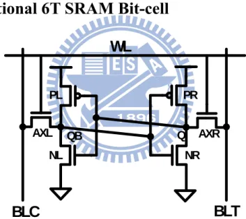
2.2.3 Conventional 6T SRAM Bit-cell
Q QB
WL
BLT
BLC
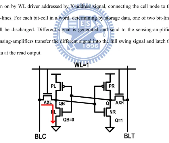
PL PR NL NR AXL AXRFig.2. 3 Schematic of conventional 6T SRAM bit-cell
Fig. 2.3 shows the schematic of conventional 6T SRAM bit-cell. This SRAM cell consists of two cross-coupled inverters (PL, PR, NL and NR), two pass-gate (AXL and AXR) transistors, one word-line and two complementary bit-lines. Two cross-couple inverters store the binary data and pass-gate transistors provide read/write access into the cell. Word-line controls the bit-line pair connecting to cross-couple inverter by turning on pass-gate transistors M5 and M6. Fig. 2.4 shows the layout view of this 6T
SRAM bit-cell.
Fig.2. 4 Layout view of conventional 6T SRAM bit-cell [2.2]
Fig. 2.5 shows the read operation of conventional 6T SRAM bit-cell. When read operation occurs, both BLC and BLT are pre-charged to VDD initially, and then WL is turn on by WL driver addressed by X-address signal, connecting the cell node to the bit-lines. For each bit-cell in a word, determining by storage data, one of two bit-lines will be discharged. Different signal is generated and send to the sensing-amplifier. Sensing-amplifiers transfer the different signal into the full swing signal and latch the data at the read output.
Fig.2. 5 Read operation of conventional 6T SRAM bit-cell
two bit-lines is pulled down by write driver determined by input data and WL is turn on by WL driver addressed by X-address signal, connecting the cell node to the bit-lines. Once one of two bit-lines is pulled down and word-line is turn on, data will be flipped and then latched by cross-coupled inverter. Finally input data is written into the cell node.
Fig.2. 6 Write operation of conventional 6T SRAM bit-cell
2.3 SRAM Bit-cell Stability and Write-ability
2.3.1 Static noise margin
During stand-by mode, the WL of the 6T cell is low so that the pass-gate transistor is off. The cross-coupled inverters must maintain bi-stable operating point to properly hold the data. The best common way to measure the stability of cross-coupled inverters is the static noise margin (SNM) [2.3]. We defined Hold SNM as the maximum DC noise voltage which is placed to the gate and the Q/QB of cross-coupled inverters which can be tolerated by the SRAM cell. In other words, hold SNM is the value of the maximum voltage which is placed between the gate and the Q/QB of cross-coupled inverters which can maintain the storage data of the SRAM cell. Fig. 2.7 shows the
setup schematic for measuring the Hold SNM. VN is the DC noise source which is placed to the gate and the Q/QB. When VN is increased, the Hold SNM of cell is changed.
Fig.2. 7 The standard setup of measuring the Hold SNM
Fig. 2.8 shows the butterfly curve, which is the most common way to represent the SNM graphically. The butterfly curve contains the voltage transfer characteristic (VTC) of one of cross-coupled and inverse VTC of the other inverter. The SNM is defined as the length of the side of the largest square which can be fit into the eyes of the butterfly curve.
Fig.2. 8 Butterfly curve of Hold SNM (Conventional 6T SRAM cell) [2.3]
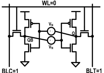
hold the data when read operation. The best common way to measure the read stability is the read static noise margin (RSNM) [2.3]. The definition of SNM is defined in the previous section. Fig. 2.9 shows the setup schematic for measuring the Read SNM. WL is on for reading access; BLC and BLT are both set to VDD to indicate the initial condition of read access.
Fig.2. 9 The standard setup of measuring the Read SNM
In conventional 6T cell, read SNM is worse than hold SNM. When read operation, WL is turn on and one of two bit-lines is discharge to a lower voltage. The “0” node will rise a little voltage because of the voltage diving effect between the pass transistor and pull-down transistor. Once the disturb voltage rise near to the trip point of the inverter, data will be flipped. Fig. 2.10 shows the butterfly curve of read SNM and hold SNM of conventional 6T SRAM bit-cell, revealing read SNM is worse than hold SNM in conventional 6T SRAM bit-cell.
2.3.2 Write trip point
Although there are many way to measure the write-ability of SRAM bit-cell, find the write trip point (WTP) is the most common and easiest way to measure the write-ability of SRAM bit-cell. WTP is defined as the maximum voltage on the BL which can make the data in the cell be flipped. Fig. 2.11 shows the setup schematic for measuring the WTP. Fig. 2.12 shows the result of finding the WTP. We fix one of the two bit-lines at high voltage and sweep the other bit line from VDD to GND, trying to flip the data in the cell. Once bit-line is lowered to a certain level, data will be flipped, indicating a successful write access. Larger WTP indicates the smaller voltage we need to lower bit-line voltage below VDD for a successful write. If the WTP value is negative, it means that although we lower the voltage of bit-line to GND, the data will not be written in. It is impossible to write data into the cell when WTP is negative, unless we can lower the bit-line voltage to negative level. We make a conclusion that higher WTP represents the better write-ability.
VBL(V)
Internode voltage (V)
Fig.2. 12 Write trip point (WTP) of conventional 6T SRAM bit cell [2.7]
2.3.3 The disadvantage of 6T SRAM Bit-cell
In 0.35, 0.18 and 0.13 μm CMOS process, 6T SRAM Bit-cell is the main structure in embedded memory. Due to some disadvantages, 6T SRAM bit-cell is not suitable under 90nm process. It is also not suitable in low-voltage operation.
First is read and half-select disturbs. The reason of generating read disturb is introduced in previous section. Furthermore, in advanced process and low-voltage operation, threshold voltage variation maybe makes the disturb voltage larger than the trip voltage of the other inverter, which can cause losing the original data in the bit-cell. In additional, there is a half-select disturb in interleaving SRAM structure. When a read/write operation, one of word-lines is turn on, the half-select cells in the same row are also doing pseudo read operation, where read-disturb also occurs. Fig. 2.13 shows the read-disturb of 6T SRAM bit-cell under different process. Cell-switch point voltage and read-down level voltage may overlap under 90nm process.
Fig.2. 13 The read-disturb of 6T SRAM in different process [2.8]
The second is the conflicting requirements between different operations. During stand-by mode, if we want to improve the cell stability, we can higher the trip point of inverters by making the pull-down transistors weaker and pull-up transistors stronger. We define this ratio as β1 ratio. To improve read SNM and minimize read-disturb, we can make the pull-down transistors stronger and the pass-gate transistors weaker. We define this ratio as β2 ratio. To improve the write-ability of SRAM cell, we can make the pull-up transistors weaker and the pass-gate transistors stronger. We define this ratio as β3 ratio. We can find that one of three β ratios is conflict to each other β ratios, as Fig. 2.14 shows. As mentioned, conventional 6T SRAM cell is susceptible of large PVT variation and local VT mismatch in advanced process. Enlarge β2 and β3 ratio can stabilize the 6T SRAM bit-cell but increased much more area and consume much more power.
Consequently, the tradition 6T bit-cell stability (Hold SNM and Read SNM) and write-ability will degrade dramatically in low-voltage due to the PVT variation and local VT mismatch. Fig. 1.3 shows this result. In addition, as mentioned in chap 1.2, Ion/Ioff ratio decrease dramatically when operating voltage is scaled down. In summary, the VDDmin of 6T SRAM bit-cell is limited to high voltage (e.g. >0.8V at 65nm)
2.4 Power Dissipation
As equation (1.1), power dissipation in CMOS circuit is composed of three main components, dynamic power dissipation, leakage power dissipation, and short-circuit power dissipation. Each kind of power dissipation will be introduced in the following.
2.4.1 Dynamic Power Dissipation
Fig. 2.15 shows a CMOS inverter with loading capacitance CL. The average dynamic power dissipation can be obtained by summarizing the average dynamic power of NMOS and PMOS. The primary dynamic dissipation component is charging and discharging the load capacitance. Suppose the operating frequency of inverter is f and the input Vin is a square wave with a period T, the load capacitance CL will be charged and discharged T * f times. In one complete charge and discharge cycle, a total charge of Q = CL *VDD will be charged or discharged in the CL. The average dynamic power of this inverter is given by
T DD DD T out P T out N D i t dt T V dt V VDD t i T dt V t i T P 0 2 / 0 2 / 0 ) ( ) )( ( 1 ) ( 1 (2.1)Where we can replace
TDD t dt
i 0
)
( to the total charge of the loading capacitance
f V C
PD L DD2 (2.2)
Because gates usually do not switch every cycle, we must consider switching probability; thus we add a switch factor α into equation 2.2. Dynamic power can be expressed as
f V C
PD L DD2 (2.3)
From equation 2.3, we know that dynamic power of logic gates is proportional to the square of supply voltage, switch factor, operating frequency and loading capacitor.
Fig.2. 15 Circuit diagram of inverter
2.4.2 Leakage Power Dissipation
As shown in Fig. 2.16 I1 is Reverse-bias PN-junction current; I2 is sub-threshold current; I3 is gate oxide tunneling current; I4 is gate hot-carrier injection current; I5 is gate-induced drain current and I6 is channel punch-through current. The mentioned six current are composed of leakage current in CMOS transistors. Sub-threshold current, gate-induced drain current and punch-through current are off-state leakage mechanisms, while Reverse-bias PN-junction current and oxide tunneling current are on-state leakage mechanisms. Gate hot-carrier injection current can occurs either in off-state or
during the transistor bias states in transition. Each source of leakage current will be introduced in the followings.
Fig.2. 16 Leakage current in NMOS transistor [2.13]
Reverse-bias PN-junction Current
Drain and source to well junctions are typically reversing biased, causing PN junction leakage current. There are two main components of a reverse-bias PN junction current, one is minority carrier diffusion/drift near the edge of the depletion region; the other is due to electron-hole pair generation in the depletion region of reversed-biased junction. In nano-scale MOSFETs, due to the use of high junction doping, large junction band-to-band tunneling (BTBT) occurs with drain at VDD and substrate at ground. The junction BTBT exponentially increases with an increase in the drain-to-substrate bias. We model Reverse-bias PN-junction current as following
)) ( exp( 0 JN DD db jn jn I V V I (2.4)
Where Ijn0is the junction leakage at Vdb = VDD and JNis a doping dependent
factor. The area of the drain diffusion and the leakage current density has impact on Reverse-bias PN-junction current, which are determined by the doping concentration.
Sub-threshold or weak inversion conduction current flowing from drain to source during the Vgs is below the threshold voltage (off-state). In the weak inversion, the minority carrier is small, but not zero. For the NMOS transistor, even if Vgs = 0V, there is still a current path in the channel of the NMOS transistor due to the VDD potential of the VDS. Unlike the strong inversion region in which the drift current dominates, the sub-threshold current is dominated by the diffusion current. Due to short-channel effect, the sub-threshold current increases with an increase in the drain bias (Drain Induced Barrier Lowering) and a reduction of channel length (VTH-roll off). Due to the body effect, the sub-threshold current reduces with the application if the reverse body-bias. We model the sub-threshold current as following
) / ) ( exp( 0 q mkT V V V V I
Isub sub gs DIBL DD bs body bs (2.5)
Where, Isub0 is the sub-threshold current of a transistors at Vgs = 0V, Vds = VDD and Vbs = 0, DIBL is the DIBL coefficient, body is the body-effect coefficient and m is
the sub-threshold swing factor.
Sub-threshold current roughly increases by a factor of five at each new technology. Such increase is due to the scaling of sub-threshold voltage and short-current effect, caused by gate length reduction. In summary, sub-threshold current becomes the biggest source of leakage current in modern transistors.
Gate oxide Tunneling Current
Gate oxide tunneling current in transistors with ultra-thin gate oxide is due to the direct tunneling of electrons (or holes) through the gate dielectric. Oxide tunneling current increases exponentially with reduction in the oxide thickness and increase in the electric field across the oxide. Fig. 2.17 shows the components of Oxide tunneling current in a scaled NMOS transistor.
Fig.2. 17 Components of tunneling current [2.13]
Gate oxide tunneling current is composed to the three elements:
1. Major components of oxide tunneling current are gate to source/drain overlap region current (Igdo and Igso).
2. Gate-to-channel-current (Igc), which goes to the source (Igcs) or to the drain (Igcd)
3. Gate-to-Substrate current (Igb)
Therefore, the gate oxide tunneling current can be divided into the following components
1. Gate-to-source (Igs = Igso + Igcs) 2. Gate-to-drain (Igd = Igdo + Igcd) 3. Gate-to-substrate (Igb)
The overlap current dominates the gate oxide tunneling current in the “OFF” state whereas gate-to-channel dominates the gate oxide tunneling current in the “ON” state. We model gate oxide tunneling current as following
) ( ) ( 0 ) ( 0 [ gON DD gd gON DD gs gd DD gOFF V V V V gON gON V V gOFF gOFF e e I I e I I (2.6)
0 gON
I is the ON state gate-to-drain leakage at |Vgs| = VDD. The magnitude of the gate leakage current increases exponentially with the gate oxide thickness Tox and the Vgs as shown in Fig. 2.18 and Fig. 2.19, respectively. [2-14]
Fig.2. 18 Gate leakage current vs. gate oxide thickness [2.14]
Fig.2. 19 Gate leakage current vs. gate voltage [2.14]
Gate hot-carrier Injection Current
In the short-channel transistor, because of high electric field near the Si–SiO2 interface, electrons or holes can get sufficient energy from the electric field to field to cross the interface potential barrier and enter into the oxide layer. This is known as the gate hot-carrier injection current.
This current from drain to bulk is caused by high electrical fields in the gate-drain overlap region. Gate-induced drain current occurs in large VDB and generates carriers into the substrate and drain from surface traps or band-to-band tunneling. Thinner oxide thickness and higher VDD enhance the electric field and therefore increase GIDL. In addition, at low drain doping, the electric field is not too enough to cause tunneling. By contrast, at very high doping, the depletion width and tunneling volume is restricted, causing less GIDL. In summary, GIDL is worse for moderated drain doping.
Channel Punch-through Current
In short-channel devices, due to the proximity of the drain and the source, the depletion regions at the drain-substrate and source, the depletion regions at the drain-substrate and source-substrate junctions extended into the channel, As the channel length is reduced, if the doping is kept constant, the separation between the depletion region boundaries decreases. An increase in the reverse bias across the junctions (with increase in VDS) also pushes the junctions nearer to each other. When the combination of channel length and reverse bias leads to the merging of the depletion regions, channel punch-through current have occurred.
Leakage current in Tradition 6T SRAM bit-cell
Fig. 2.20 shows all kind of leakage current in conventional 6T SRAM bit-cell, including sub-threshold leakage, gate leakage and junction leakage. Since most of the SRAM bit-cell in SRAM array is usually on the stand-by mode, leakage power dominates the total power consumption of SRAM. Considering the different leakage components of all transistors, we can count the total leakage of the cell as following
gate jn sub leak NL gOFF PL gOFF NE gON PR ON g AXR gOFF AXL gOFF gate jnPR jnNL jnAXR jnAXL jn subPR subNL subAXR sub I I I I I I I I I I I I I I I I I I I I _ _ _ _ _ _ 2 2 2 (2.7)
2.4.3 Short-circuit Power Dissipation
Short circuit power dissipation occurs as both pull-up and pull-down networks are partially ON while the input switches, existing a direct path current flowing from the power supply to the ground. It increases as edge rates become slower because both networks are ON for more time. It decreases as load capacitance increases because with large loads the output only switches a small amount during the input transition, leading to a small VDS across one of the transistors. Short current power dissipation can be expressed as
DD mean SC I V
P (2.8)
Where Imean is the mean value of the short circuit current, and Imean is modeled as [2-15]: T V V V P DD T DD SC ( 2 )3 12 1 (2.9)
Where β is the gain factor of a transistor, τ is the input rise/fall time. Although this is a simplified model, it reveals the fact that short current is affected by operating voltage, rising time or falling time of input signal, threshold voltage and operating frequency. In summary, decreasing operating voltage and rising/falling time of input
signal and increasing threshold voltage decrease short-circuit power dissipation.
2.4.4 Total Power Dissipation
As we mentioned in the previous section, we can make a conclusion of total power as following circuit short dynamic leakage total
P
P
P
P
(2.10)All kinds of power dissipation are relative to the operating voltage VDD. Last but not the least, because of operating voltage VDD dominating total power consumption, lowering the operating voltage VDD is the most effective way to reduce the total power consumption.
2.5 Recent Low-voltage SRAM Bit-cell Design
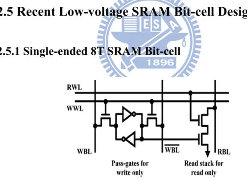
2.5.1 Single-ended 8T SRAM Bit-cell
Fig.2. 21 Single-ended 8T SRAM bit-cell [2.6]
Fig. 2.21 shows this single-ended 8T SRAM bit-cell. This cell added two extra transistors as read buffer, which make cell node decoupled from RBL. Consequently, this cell is read-disturb free and the read SNM of the cell is much better than conventional 6T cell. Because of the separation of read-port and write-port like register
files, we can improve read-stability and write-ability without conflicting requirement. By using single-ended read port and hierarchical BL scheme. This cell is designed in a high-performance 32kb sub-array in 65nm PD-SOI CMOS process and can operate at 5.3GHz in 1.2V and 295MHz at 0.41V. Fig. 2.22 shows the improvement of Read SNM between this 8T cell and conventional 6T cell
Fig.2. 22 Read SNM of conventional 6T-SRAM & single-ended 8T-SRAM [2.6]
One of ISSCC 2010 paper about Core Implemented contributed by AMD [2.16], it said that single-ended 8T SRAM is commonly used in recent single-VCC microprocessor core for its performance critical low-level caches and multi-ported register-file arrays. However in write operation, once one WWL is pulled-up, all of pass-gate transistors in the same row are turn on. Because of full VDD on WBL and WBLB which are pre-charged in stand-by mode, so once WWL is pulled-up, stored node will be affected by BL, called pseudo read or Half-select disturb. In summary, this 8T cell eliminates read-disturb, improving the read SNM. But this 8T cell still suffers from Half-select disturb.
conventional SRAM cell, the cross-coupled inverter of this cell is supplied by bit-line pair instead of sharing the same power lines. Fig. 2.22(b) and (c) shows the waveform of read and write operations.
Fig.2. 23 (a) The schematic of D2AP 8T cell (b) waveform of write operation (c) waveform of read operation [2.17]
In stand-by mode, ZWL=0, both BL and BLB are pre-charged to VDD and VDDL and VDDR are pre-charged to VDD through PSWL and PSWR. In write-0 operation, ZWL = 0, WL = 1 and BL is pulled-down to 0, VDDL is reduced by PSWL, which improve the write-ability in write-0 operation. In contrast, in write-1 operation ZWL = 0, WL = 1 and BLB is pulled-down to 0, VDDR is reduced by PSWR. In read operation, ZWL and WL are VDD. There is an additional discharge path through PSW and PU transistors either read-1 or read-0. Due to additional discharge path and differential read scheme, the noise immunity and read access time is better than single-ended 8T cell. In
half-select cell, self-negative feedback can reduce VDDL or VDDR, lowering the trigger point of inverter and providing a better cell stability. The disadvantage of this cell is floating “1” on un-selected row because of ZWL = 1. A 39Kb sub-array is designed in 45nm process. The VDDmin is 540mV, 200~240mv better than single-ended 8T SRAM in same array structure.
2.5.3 A Large σVTH/VDD tolerant zigzag 8T SRAM (Z8T)
Fig.2. 24 Schematic of Z8T SRAM cell (b) Layout view of Z8T SRAM cell [2.18]
Fig. 2.24 shows the schematic and layout of σVTH/VDD tolerant zigzag 8T SRAM. In stand-by mode WWL=0 and RWL =1 so both BL and BLB is clamped to VDD through un-selected NR0 and NR1, reducing the BL leakage current. This Z8T cell can have long BL structure.
When read-operation, WWL =0 and RWL = 0. RBL and RBLB will be discharged according to data in the selected cell. Because of cell node decoupled from RBL, the Read SNM of Z8T cell will be improved. The write-operation is similar to conventional 6T cell. A 32Kb sub-array with this Z8T cell is designed in 65nm process. Hierarchical WL structure and differential read and write-back sense amplified are used. The
2.5.4 A Novel Column-Decoupled 8T Cell (CDC-8T)
Fig.2. 25 Selected and half-selected cell of CDC-8T [2.19]
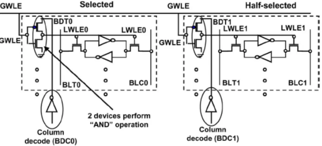
Fig. 2.25 shows the selected cell and half-selected cell of this CDC-8T, which can eliminate half-select condition. On selected cell, GWLE is 0 and BDT0 is 1, so LWLE0 is 1 during read or write operation. On the half-selected cell, GWLE is 0 but BDT1 is. LWLE1 is 0. By this column-decoupled scheme, read half-select disturb can be eliminated. This CDC-8T cell can also be interleaved to solve the soft-error-rate problem by using simple ECC. The half-select free design enables further voltage scaling. The VDDmin of this cell is 150mv smaller than conventional 6T cell in 1.6Kb sub-array in 90nm PD/SOI process. [2-19]
2.5.5 Schmitt-Trigger-Based SRAM Design (ST cell)
Fig. 2.26 shows a Schmitt-trigger-based SRAM bit-cell (ST cell). In hold operation, due to stack pull-down transistors, the hold SNM is better than conventional 6T cell. Input-dependent transfer characteristics of Schmitt-trigger improve both read-stability and write-ability. Furthermore, the storage node is isolated from the BL/BR because the WWL is off during read. It can improve read stability-too. In write
operation, there are two discharge paths through AXL1/AXR1 and AXL2/AXR2 which can improve write-ability, too. This ST cell proposed 1.6X read-stability, 2X write-ability and 120mv lower read VDDmin compared to iso-area conventional 6T bit-cell in 130-nm CMOS process [2-2][2-20]
Fig.2. 26 ST SRAM bit-cell schematics [2.2] [2.20]
2.5.6 Column Line Assist 10T SRAM cell (CLA-10T)
Fig.2. 27 CLA-10T SRAM (a) schematic (b) layout [2.21]
Fig. 2.27 shows the schematic and layout of CLA-10T cell. The Read SNM is worse than previous bit-interleaving 10T SRAM [2-22] because both outside and inside
pass-gate transistors are pulled-up to VDD when read operation and cell-node is not decoupled of BL. When read operation, WL is pulled-up to VDD, BL and BL/ are pre-charged to VDD in advance and CL and CL/ are pulled down to GND. The read current is larger than prior 10T SRAM due to an additional discharging path from BL to CL.
In write operation, WL is VDD. One of BL pair will be discharged to GND, same as CL pair. There is an additional path from CL to cell node which improves the write-ability of this CLA-10T cell. A 128Kb CLA-10T SRAM array is designed in 45nm process. The VDDmin is 0.56V.
2.6 Recent Read/Write Assist Circuit Technique in
Low-Voltage SRAM Design
In low-voltage SRAN Design, sometimes creating novel bit-cells in low-voltage SRAM is not sufficient. We also need some read or write assist circuit technique, such as single-ended sensing improvement circuit, negative bias on BL or VSS of bit-cell and suppressing or under-driving either the VDD of bit-cells or the voltage of word-lines. We will discuss recent R/W assist circuit technique as following section.
2.6.1 Single-ended Sensing Innovation
Some alternative SRAM bit-cells, such as single-ended 8T SRAM [2.6], use the single-ended sensing scheme. Compared to differential sensing scheme, single-ended sensing scheme is slower due to full VDD swing. As mentioned, single-ended sensing scheme is more sensitive to have read failure in low-voltage SRAM Design.
There are some single-ended sensing innovations in Fig. 2.28. Fig. 2.28 (a) shows sense-amplifier redundancy scheme by selecting a backup sense amplifier if the original one does not work [2.23]. Fig. 2.28 (b) shows the re-configurable sensing
scheme for DVS, including NMOS input sense-amplifier and PMOS sense-amplifier. In high voltage operation, we choose NMOS input SA because inputs with a higher common-mode voltage results in faster solution of the outputs. In contrast, in low-voltage operation we choose PMOS input SA because PMOS input SA has faster resolution when common-mode inputs are close to GND [2.24]. Fig. 2.28 (c) shows the VGND replica scheme to generate the virtual GND voltage of sensing inverter in read buffer. The trip point of sensing inverter in read buffer is automatically adjusted to the midpoint between the high voltage and the low voltage of BLs [2.25]. Fig. 2.28 (d) shows the AC-coupled sense-amplifier to distinguish the sensing time between true “1” and false “1” at low-voltage operation [2.26]
2.6.2 Negative-biased Read/Write Assist Circuit
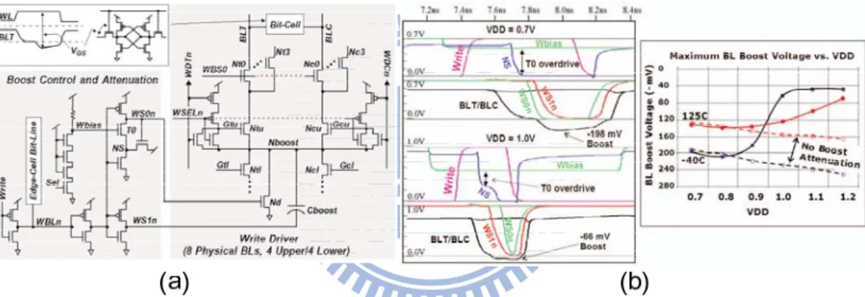
The basic concept of negative-biased read/write assist circuit is pulling-down the BL to negative voltage in write operation [2.30] and pulling-down the VSS node of bit-cell in read operation [2.27]. Fig. 2.29 shows the negative-biased Read/Write Assist circuit (schematic and waveform) of cross-point 8T SRAM. In read operation, the VSM is pulled-down to negative voltage. In write operation, one of BL pair is pulled-down to negative voltage, as shown in Fig. 2.29 (b). A 1Mb SRAM array is designed in 45nm bulk LSTP CMOS process with cross-point 8T cell and negative-biased read/write assist circuit [2.27]. The VDDmin can be reached to 0.6V. The similar concept which is used to enhance read/write ability for dual-port SRAM is also shown in Fig. 2.29 [2.28]. A 1Mb SRAM array is designed in 45nm process. The VDDmin can be improved by 120mV.
Fig.2. 29 (a) Cross-point 8T SRAM (b) Read/write negative-biased circuit (c) waveform [2.27]
Fig. 2.31 shows another way of negative-biased BL for write-ability improvement. The boost node Nboost is connects to 8 BL pairs and pre-charged to GND at the end of write cycle. The capacitor Cboost is charged to VDD when WS1n is VDD before the write cycle. In a write cycle, WS1n and WS0n are discharged to GND. In high-voltage operation, it needs not too high negative boosting efficiency. WS1n is pulled down to GND, first. The boosting efficiency is not too high. In contrast, in low-voltage operation, it needs high negative boosting efficiency. WS0n is pulled down to GND, first. The boosting efficiency is high. Fig. 2.30 (b) shows the result. The 64Mb SRAM is built from 128*512Kb Macro in 32nm High-K metal gate SOI process. The operation voltage can be scaled down to 0.7V [2-29]
Fig.2. 31 (a) Write driver with boost control (b) Waveform of write cycle [2.29]
Fig. 2.32 shows the constant-negative-level write buffer, the charge in C_boost is proportional to the BL capacitance. It means that the charge in C_boost is proportional to the cells per bit-line. It generates a constant-negative-level in BL during write operation. The target bias level is -0.15V±0.05V, which is not too negative to hold the data in un-selected cell and not too low to write the data into the selected cell. Fig. 2.31(b) shows the automatically optimized constant negative BL level for 4 cells per bit-line and 512cells per bit-line [2.31]
2.6.3 Voltage modulation Read/Write Assist Circuit
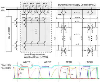
The basic concept of voltage modulation R/W Assist Circuit is that we can boost WL voltage or suppress the VDD voltage of the cell array to enhance the write-ability. In contrast, we can suppress the WL voltage or boost the VDD voltage of the cell array to enhance the read-stability. Fig. 2.33 shows level-programmable word-line driver (LPWD) and dynamic array supply control which can tune the WL voltage and array supply voltage in read and write cycle, respectively [2.32]. In single-ended 8T SRAM, due to the separation of read port and write port, we can boost RWL in read cycle and boost WWL in write cycle, respectively, as shown in Fig. 2.34 (a). It also use write-back scheme to solve the half-select read disturb problem. A 64Kb 8T-SRAM is designed in 90nm process. VDDmin can reach to 0.42V and area overhead is 8.5% [2.33]
Fig.2. 33 Level-programmable word-line driver (LPWD) and dynamic array supply control (DASC) [2.32]
Fig.2. 34 (a) Boost RWL and WWL in read/write cycle (b) Write back scheme [2.33]
Fig. 2.35 shows the R/W assist circuits, respectively. Fig. 2.35 (a) shows the WL under-drive circuit to improve the read stability. Fig. 2.35 (b) shows the write assist circuit that can lower the voltage of SRAM array supply during write cycle. A 512Kb conventional 6T SRAM array is designed in 45nm bulk process. The VDDmin is improved from1.13V to 0.96V [2.34]. Due to suppressing the VDD source of WL driver, the rise time of WL is slow in Fig. 2.35(a). Fig. 2.36(a) shows a modified WL
under-drive circuit. The rise time of Fig. 2.36 (a) is 60% faster than Fig. 2.35(a) [2.31].
Fig.2. 35 (a) Word-line under-drive circuit (b) Write assist circuit [2.34]
Fig.2. 36 (a) Modified Word-line under-drive (WLUD) circuit (b) Rise time of WLUD circuit [2.31]
Fig. 2.37 shows another way of word-line under-drive circuit called as the adaptive dynamic word-line under-drive (ADWLUD) circuit which consists of WLUD module, controller and 6T SRAM bit-cell based sensor. It can adaptively tune the strength of WLUD circuit on different PVT condition. Conventional 6T cell based Vtp/Vtn sensor will adaptively track the different PVT condition to generate the Vsensor. Vsensor is compared to Vref1 and Vref2. If Vsensor < Vref1, the small PMOS P3 is turn on for applying a strong WLUD. If Vsensor < Vref2 the large PMOS P4 is turn on for applying a weak WLUD. The reference voltage generation circuit consists of a resistive divider with a multiplexer for controller calibration. A 3.4Mb SRAM macro is designed in 32nm high-k metal gate process. The VDDmin is improved by 130mV [2.35].
Fig. 2.38 shows the schematic and waveform of multi-step word-line control technology. This technique improves not only SNM and also write-ability. First we pull up P1 and P2 to VDD by asserting the CLK_WL. The WL capacitance C is gradually charged to VDD. The slow WL rise improve the SNM of half-select cell by suppressing the read-disturb voltage. After WL voltage is reached to 1.0V, CLK_PU is activated and the WL capacitance C is boosted to 1.1V with the pumping capacitor Cp. The write-back speed of half-select cell can be speed up.
We need to determine the PMOS resistor R and the pumping capacitor Cp. If R is too small, the worst SNM of half-select cell can’t retain the data because WL voltage will reach 1.0V before BL voltage is discharged to a level at which SNM will remain true. If R is too big, the operating speed of SRAM will be too late. Cp is determined that can generate a sufficiently high voltage for stable write operations. [2.36]
Fig.2. 38 Multi-step word-line control technology for word-line drover [2.36]
2.7 Summary
This chapter first introduces the structure and basic operation of conventional 6T SRAM and then introduces the basic concept and measurement of stability and write-ability in SRAM bit-cell. Power dissipation, such as dynamic power dissipation, leakage power dissipation and short-circuit power dissipation are discussed. We know that leakage power dissipation becomes a critical issue of SRAM design in advanced process. Some alternative SRAM cells in low-voltage consisted of 8T or 10T are also introduced in this chapter. Finally we introduce some read/write assist circuit to improve the cell stability, read/write speed and write ability in low-voltage SRAM design. The R/W assist circuitry is usually based on the concept of negative-biased voltage and voltage modulation on BL/WL voltage, the VDD or VSS of the cell array. Obviously the conventional 6T SRAM can’t satisfy the demands in low-voltage region. Following chapter will present an 8T SRAM bit-cell with data-aware write-assist topology and ripple BL sensing scheme and local BL keeper design.
Chapter 3
A Low VDD
MIN
Date-aware Write-Assist 8T
SRAM with Adaptive Write-time Tracing
Replica Circuit
3.1 Introduction
As we discussed in Chap 1 and Chap 2, conventional 6T is not suitable in nano-scale process due to the critical variation of process and temperature. In [3.1], authors point out that the area of 6T bit-cell will be larger than 8T bit-cell in advanced process because we need large beta and gamma ratio to cope with process and temperature variation, as shown in Fig. 3.1. Conventional 6T is not suitable in low-voltage region due to read-disturb problem, half-select disturb problem and not sufficient SNM. It is difficult to lower the VCCMIN of conventional 6T bit-cell. Consequently, it is necessary to find an alternative SRAM bit-cell topology to work in advanced process and low-voltage
In this chapter, an 8T SRAM bit-cell with data-aware write-assist (DAWA) will be presented. Cell structure and basic operation will be introduced, first. And then the cell-stability and write-ability of this DAWA 8T cell will be discussed in detail. The architecture of this 8T cell-array will be presented. Finally an adaptive write-time tracing replica circuit, adaptive VVSS driver and WWL driver using in this 8T cell will be presented. Following simulation and analysis are based on UMC 40nm LP process. This projected are discussed with supported by professor Ching-Te Chuang of Digital VLSI Lab, Hao-I Yang of LPMD Lab and the IPD department of Faraday Technology
Corporation.
3.2 Cell Structure and Basic Operation of Cell
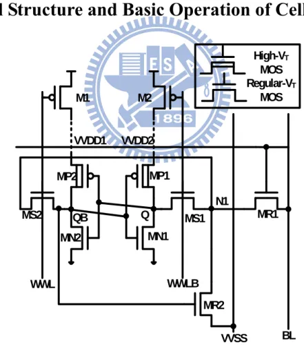
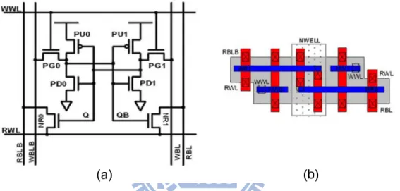
WWLB WWL QB Q VVSS VVDD1 VVDD2 M1 M2 MP1 MP2 MN1 MN2 MS1 MS2 MR2 BL MR1 Regular-VT MOS N1 High-VT MOS
Fig.3. 2 Schematic of DAWA 8T cell
Fig. 3.2 shows the schematic of 8T cell with data-aware write-assist (DAWA) scheme, this cell have outer layer pass-gate MR1 and inner layer pass-gates MS1/MS2.
Outer pass-gate MR1 is controlled by row-based WL. Inner pass-gates MS1 and MS2 are controlled by column-based signal WWL and WWLB, respectively. WWL, WWLB and VVSS are determined by input data when write operation. M1 and M2 are power switches of this 8T cell which are shared by several cells per column. There is only one BL in this 8T cell, so this cell is single-port structure that can reduce power consumption. In addition to data-aware write-assist scheme, this 8T cell uses High-VT PMOS to weaken PMOS transistors of cross-coupled inverters, improving the write-ability. Furthermore the High-VT PMOS can reduce the leakage current in bit-cell. In summary, this 8T bit-cell is Dual-VT and single-port bit-cell. The layout views of this 8T cell in UMC 40nm LP process is in Fig. 3.3. The column-based signal such as WWL, VVSS, VVDD1, VVDD2, BL and WWLB are routed in metal 2. The row-based signal such as WL, GND and inter-node N1 are routed in metal3. One 8T bit-cell size in UMC 40nm LP process is 1.44μm x 0.59μm = 0.85μm2
3.2.1 Pre-charged / Stand-by Mode
In pre-charged or stand-by mode, since WL, WWL and WWLB are turned off the inner pass-gates MS1/MS2 and outer pass-gates MR1 are turned off, improving the stability of the bit-cell, as shown in Fig. 3.4. Since WWL & WWLB are logic “0”, both power switch PMOS transistors M1/M2 are turned on, keeping VVDD1 & VVDD2 on full VDD. In pre-charged mode, the voltage level of BL is VDD and the voltage level of VVSS is GND during pre-charge or stand-by operation
WL= 0" WWLB= 0" WWL= 0 QB Q VVSS= 0" VVDD1 VVDD2 M1 M2 MP1 MP2 MN1 MN2 MS1 MS2 MR2 BL= 1" MR 1 N1
Fig.3. 4 Pre-charged / stand-by mode of DAWA 8T bit-cell
3.2.2 Read Mode
In read operation, BL is pre-charged to VDD in advanced. The voltage of VVSS is GND. Column-based signal WWL and WWLB are GND. The row-based signal WL is pulled-up to VDD so that the outer pass-gate MR1 is turned on. BL is kept at VDD if QB is logic “0” and discharged to GND through MR1 and MR2 if QB is logic “1”. Read
operation in the DAWA 8T bit-cell is same as conventional 8T bit-cell. Read disturb is eliminated. Both power switch PMOS transistors M1/M2 are turned on, keeping VVDD1 & VVDD2 on full VDD. Fig. 3.5 shows the read operation.
Fig.3. 5 Read mode of DAWA 8T bit-cell
3.2.3 Data-aware Write-assist Write Mode
In write operation, BL is discharged to GND first. The row-based signal WL is pulled-up to logic “1” so that the outer pass-gate MR1 is turned on. The column-based signal either WWL or WWLB is pulled-up to VDD determined by the data which we want to write into the selected cell. When we want to write logic “1” into the cell node, WWL is pulled-up to VDD. When WWL is logic “1”, the power switch M1 is turned off, making the node VVDD1 floating. Floating VVDD1 weakens PMOS transistors MP2 and then logic “1” is easier to write in the selected cell. In contrast, when we want to write logic “0” into the cell node, WWLB is pulled-up to VDD. When WWLB is logic “1”, the power switch M2 is turned off, making the node VVDD2 floating. Floating
selected cell. This is data-aware write-assist write operation.
Next we consider the column-based signal VVSS. In write “1” operation, if VVSS is logic “0”, disturb happened on the column half-selected cells whose cell node QB store data “1” in the same column. The discharging path is through from QB, MS2 and MR2 to VVSS and then the logic “1” in QB of the column half-selected cells may be discharged to logic “0”. In contrast, in write “0” operation, if VVSS is logic “1”, disturb happened on the column half-selected cells whose cell node Q store data “0” in the same column. The discharging path is through VVSS, MR2 and MS1 to Q and then the logic “0” in Q of the column half-selected cells may be charged to logic “1”. As shown in Fig 3.6. Thus we must set VVSS to logic “1” when write “1” operation and set VVSS to logic “0” when write “0” operation. Fig. 3.7 show the write “1” operation and write “0” operation when VVSS is connected to logic “1” and logic “0”, respectively. In addition, Write “1” is more critical than write “0”
![Fig. 2.27 shows the schematic and layout of CLA-10T cell. The Read SNM is worse than previous bit-interleaving 10T SRAM [2-22] because both outside and inside](https://thumb-ap.123doks.com/thumbv2/9libinfo/8420755.180503/41.892.140.676.241.723/schematic-layout-worse-previous-interleaving-sram-outside-inside.webp)