國
立
交
通
大
學
電機與控制工程系
碩
士
論
文
利用混沌產生器抑制直流-直流轉換器
電磁干擾水平
Suppression of Electromagnetic of DC-DC Converter
with Chaos Generator
研 究 生:沈柏年
指導教授:陳福川 教授
利用混沌產生器抑制直流-直流轉換器
電磁干擾水平
Suppression of Electromagnetic of DC-DC Converter
with Chaos Generator
研 究 生:沈柏年 Student:Po-Nien Shen
指導教授:陳福川 Advisor:Fu-Chuang Chen
國 立 交 通 大 學
電 機 與 控 制 工 程 系
碩 士 論 文
A ThesisSubmitted to Department of Electrical and Control Engineering
College of Electrical Engineering
National Chiao Tung University
in partial Fulfillment of the Requirements
for the Degree of
Master
in
Electrical and Control Engineering
September 2008
Hsinchu, Taiwan, Republic of China
利用混沌產生器抑制直流-直流轉換器電磁干
擾水平
研究生:沈柏年 指導教授:陳福川 教授 國立交通大學 電機與控制工程研究所摘要
在對於電子產品上,DC-DC 電源轉換器是一種電磁干擾源;因此對於開關
式電源轉換器的設計,抑制電磁是一個很重要的課題。傳統抑制電磁干擾
的方法利用 LC 濾波器跟金屬屏蔽來達到抑制效果,但是此方法會增加系統
成本,體積跟重量。在這此論文裡,我們提出的方法是利用混沌特性來降低
由開關式電源轉換器所產生的電磁干擾峰值並且把諧坡的離散頻率分散成
連續的多頻特性。此方法主要將依賴混沌特性所調變的時脈來影響一個操
作原本正常週期的電源轉換器。最後的穩定度分析與模擬結果證明此方法
對於抑制電磁干擾是非常有效的並且不影響電源轉換器的性能。此外,有
別於其他方法,此方法可以很容易的應用在 CMOS 技術上。
Suppression of Electromagnetic of DC-DC
Converter with Chaos Generator
Student:Po-Nine Shen Advisor:Dr. Fu-Chuang Chen
Institute of Electrical and Control Engineering
Nation Chiao Tung University
ABSTRACT
Power DC-DC converters are notorious sources of electromagnetic interference in electronic
products; therefore, suppression of EMI is an important topic in the design of switch-mode
power converters. Conventional EMI suppression methods may employLC filters and metal
shielding, but this can significantly increase cost, size, and weight. In this paper we propose
a chaos-based method to reduce peak EMI magnitude and spread the energy to a wide range
of frequencies.This method is to add a chaos-modulation clock to a converter maintaining in
regular period state, in order to create chaotic behaviors in the converter. Our results show
that this method is effective in suppressing EMI in DC-DC converters without much impact
on the performance of converters. System stability is also analyzed and discussed.
Moreover, compared with conventional methods, the method can be easily implemented in
誌謝 Acknowledgment
首先感謝我的指導教授陳福川博士在我碩士班生涯的悉心指導,除了在於研究學問 上的啟發外,也讓我解決問題的能力與心態有所進步。 此外感謝我的父母沈永森先生和蔡玉華女士,從小對於我的提攜與照顧,在我學生 生涯讓我不愁吃穿,可以專心在課業與研究上,還有我的哥哥沈柏成,妹妹沈宜蓉,謝 謝你們的關心跟支持,這份榮譽是屬於你們大家的。 感謝我的女友欣樺,在於寫論文期間對於我的關心與包容,有妳的體諒,讓我可以 專心在研究跟論文上。 感謝我的室友,火球,大鼻子,因為你們的幽默與友善,消除我在研究上的壓力。 也感謝在交大陪我一起打球的球友,讓我可以趁機活動經骨,更讓我體會到團隊合作的 默契。 感謝育宗學長在這兩年在學術上的研究對我的幫助,更提供寶貴的建議與鼓勵,還 有同實驗室的文佑,學弟們智龍,武璋以及瑞祺,謝謝你們在這些日子陪我經歷研究生 活的甘與苦。 最後要謝謝這兩年在新竹唸書期間所有幫助過我的人,雖然無法一一列舉,但在這 邊向大家致上最大的謝意。 沈柏年 2008 夏 於新竹交大Contents
中文摘要………...………….……….. I
English Abstract ... II Acknowledgment... III Contents ...IV Lists of Tables ...VI Lists of Figures ...VII
Chapter 1 Introduction………...………...1
1.1 Current Status and Background………1
1.2 Motivation and Aims………...………...3
1.3 Organization………...……….4
Chapter 2 Basic Theory of Boost Converter and Chaos………5
2.1 State Analysis of Boost Converter………..………5
2.1.1 Continuous Condition Mode(CCM)………...6
2.1.2 Boundary between CCM and DCM………...…………8
2.1.3 Discontinuous Condition Mode(DCM)………...……...9
2.2 Analysis of Discrete Model………...………12
2.2.1 Sampled Data………..12
2.2.2 Mapping………..14
2.2.3 Phase Portrait and Attractor………...….15
2.2.4 Bifurcation Diagram………..16
2.3 Model of a Boost Converter with Peak Current Control………..17
Chapter3 Design of Converters with Chaos Generator………...………21
3.1 Modeling of Chaos Generator………21
3.3 A current-controlled boost converter without chaos generators………28
3.4 A current-controlled boost converter with chaos generators…...…………...29
3.5 Analysis of Stability of a boost converter with chaos generators…………....31
3.5.1 The slopes of charge and discharge of an inductor current in a boost converter under current mode control………...………...31
3.5.2 The influence of the gain of driving circuit and current modulator...32
3.5.3 Analysis of Period-1………...………..33
3.5.4 Analysis of Period-2………...…………..35
3.5.5 Analysis of Period-4………...…………..…37
3.5.6 Analysis of Chaos………...………..39
Chapter 4 Simulation Result and Analysis………...……….42
4.1 The circuit frame of a current-controlled boost converter………..….42
4.2 Simulation of stability………...45
4.3 Response of Output Voltage to loading current……….49
4.4 Clock Times of Frequency for the clock signal………...………50
4.5 Simulation of PSD……….51
Chapter 5 Conclusion……….58
Lists of Tables
Table 2-1 The specification of a boost converter……….………….20
Table 3-1 The specifications of the chaos generator……….………25
Table 3- 2 The relation of operating states and Vs……….………..25
Table 4-1 The specifications of the boost converter in close loop………..….42
Table 4-2 Degree of reduction(Period-1 & Period-2)………...52
Table 4-3 Degree of reduction(Period-1 & Period-4)………...54
Table 4-4 Degree of reduction(Period-1 & Chaos)………...55
Lists of Figures
Fig.2-1(a) Switch-mode DC-DC conversion(b)The average output value Vo depends
on to and toff………...……….…5
Fig.2- 2 Boost Converter circuit……….……..6
Fig.2-3 Boost converter circuit states (a)switch is on (b)switch is off………...7
Fig.2-4 Waveforms of voltage and current of inductance……….….7
Fig.2- 5 the inductor current at the boundary………...….9
Fig.2-6 The circuit the boost converter operates under DCM……….……...10
Fig.2-7 The inductor current under DCM………....11
Fig.2-8 Sampling Types of control voltage and ramp waveforms under voltage mode control………..……….13
Fig.2-9 Sampling Types of the desired level and inductor current under current mode control………..……….13
Fig.2-10 Waveform sampled at constant intervals giving (a)one fixed point(b) two fixed points………....14
Fig.2-11 Illustration of a discrete mapping………...…15
Fig.2-12 The phase portrait of the buck converter………..…16
Fig.2-13 The bifurcation diagram of output and the parameterE ………16
Fig.2-14 The bifurcation diagram of the boost converter by Iref varying………20
Fig.3-1 Schematic of chaos generating circuit………..21
Fig.3- 3 The circuit frame of the new chaos generator………24
Fig.3- 4 Bifurcation Diagram of the Chaos Generator………26
Fig.3-5 The waveforms of different states in time domain.. ………...28
Fig.3-6 blocks of the close loop circuit with chaotic signal………..30
Fig.3-7 The behavior of driving circuit (a) the circuit of S-R flip-flop(b) the signals of driving circuit………..30
Fig.3-8 Inductor current waveform of the boost converter under current-mode control.. ………31
Fig.3- 9 Block diagrams of a close-loop for a power converter with current control….32 Fig.3-10 The inductor current waveform for different reference currents………....33
Fig.3-11 The inductor current waveform in period-1………..34
Fig.3-12 The inductor current waveform in a period T………...35
Fig.3- 13 The inductor current waveform in period-2……….35
Fig.3-14 The inductor current waveform in period-4………..…37
Fig. 3-15 The waveform of Q signal in period-4 state.……….37
Fig.3-15 The inductor current (clock frequency is increasing)………...39
Fig.3-16 The inductor current (clock frequency is decreasing)………..40
Fig.4-1 Circuit diagram of the current-controlled boost converter………43
Fig.4-2 The compensator……….………..….44
Fig.4-4 The circuit frame of a boost converter with chaos generator………45
Fig.4-5 Simulation in Period-1(Vs=15V)………..……46
Fig.4-6 Simulation in Period-2(Vs=12.5V) ………...………47
Fig.4-7 Simulation in Period-4(Vs=11.8V)………...………….47
Fig.4-8 Simulation in Chaos(Vs=10V)………..…….48
Fig.4-9 Simulation in Chaos during 10ms (Vs=10V)………...…48
Fig.4-10 The circuit for testing varying loading………...…49
Fig.4-11 The testing circuit of testing varying loading………49
Fig.4-12 Simulation of load current change………..50
Fig.4-13 The statistical chart of the clock times of frequency for the clock signal……....50
Fig.4-14 Simulation of PSD (Period-1 and Period-2)………...52
Fig.4-15 Simulation of PSD (Period-1 and Period-4)………...53
Fig.4-16 Amplification of simulation of PSD (Period-1 and Period-4)………….………..53
Fig. 4-17 Simulation of PSD (Period-1 and chaos)………...…….………...54
Fig. 4-18 Amplification of simulation of PSD (Period-1 and chaos)………...………55
Chapter1
Introduction
1.1
Significance of the Research
The chaos technique is an important topic for study in power electronics because many
applications employ it. At present, there are two study fields applying the chaos technique in
DC-DC converters. The first field is the control of chaos. It mainly uses small perturbations to
stabilize unstable periodic orbits which are abundant in chaotic attractors. A famous method
for chaos control strategy was reported by Ott-Grebogi-Yorke(OGY) [1]. In addition, other
methods are also proposed. For example, occasional proportional feedback method[2],
versions of OGY method[3], and time-delayed auto-synchronization method [4, 5]. The other
study field is that of reducing EMI in switching-mode power supplies which are notorious
generator of both conducted and radiated Electromagnetic interference (EMI), owing to high
rates of voltages and currents. In the paper, we focus on the problem of reducing EMI for
DC-DC converters by chaos technique.
Nowadays, a very large amount of electromagnetic emission exists, so that the problem of
designing electromagnetic compatible (EMC) systems has become a great and widespread
emission is of paramount importance. Due to the rapid switching of high currents and
voltages, interference emission may become severe. Conventional methods to tackle the EMI
problems include LC filters and metal shielding for EMI. These solutions generate their own
problems like increased cost, size, and weight. Moreover, such designs are not suitable in
different EMC norms because each time the application domain of main system changes,
filters and screens have to be redesigned even if the converter specifications themselves are
unchanged. This incurs additional expenses and increases design time [6]. In addition, a
soft-switching technique is one of the methods directly tackling the EMI problems. However,
the result that can be achieved by this method is limited[7].
Because of the quality of containing many frequencies in chaos, chaos technique can be
applied to expand frequency band in systems[8]. Moreover, it can achieve the purpose of
dispersing the energy in spectrum so that the peak values in fundamental frequency and the
harmonics are reduced. Compared with the high peak value in a narrow frequency band, the
quality of the low peak value in a wider frequency band is easy to conform to various EMC
norms. Therefore, operating under the chaos state for switching converters is practical to
improve EMC problems.
Up to now, switching converters have two methods to achieve suppression of EMI by
chaos technology. The first method is the parameter-controlling method [9-14]. Switching
and reference voltage and loading, etc. For example, converters may operate under the chaos
state when output loading is changed. Besides, the properties of converters are affected when
parameters are adjusted. Because the controlling condition is very complex, it is difficult to
achieve a satisfying design.The second method is variable- frequency-modulation method[15].
It mainly utilizes the broadband nature of clock signal generated by chaotic system to reduce
EMI. The main advantage for this method is that the system is forced into the chaos state
without changing the properties of the main system. Since the chaos generator affects the
clock signal, the proposed method of EMI reduction can be applied to any existing converters.
Some methods of spreading the spectrum through chaotic modulation have been proposed in
[16-19], However, analyses of stability are not analyzed and discussed further in above papers.
Moreover, someone employ Chua’s circuit [20-23] as a chaos generator generating chaotic
signals, but it has some difficulties in IC design, owing to an inductor element in the circuit.
1.2 Motivation
We propose a circuit frame applying the EMI reduction technique to drive a
current-controlled boost converter. The circuit frame mainly employs the characteristic of fast
charge and discharge of a capacitance to generate a set of chaotic signals. The main advantage
of the circuit frame is to be built and still achieve the purpose of suppression of EMI of a
circuit which oscillates chaotic signal by an inductor and a capacitance, it is appropriate to use
the circuit frame in VLSI regime. In the article, we will compare performances of the two
mentioned EMI reduction methodologies in terms of PDS peak reduction and the inductor
current ripple. Furthermore, in order to estimate the influence of this method on its
performance, we particularly analyze the stability of the converter in every quasi-period state
by analyzing duty ratio. The results of simulation show that every power of harmonics in an
inductor current under chaos state is reduced by more 45%.
1.3 Organization
The rest of the thesis is organized as follows. Chapter1 of the article is a review of the
literature. This is followed by the method of studying discrete models for chaos. The Chapter3
section describes the design of chaos generator and analysis of stability. The results for the
simulation analysis are presented in the fourth section. Finally, conclusions are presented and
Chapter2
Basic Theory of Boost Converter and Chaos
2.1 State Analysis of Boost Converter
DC-DC Converters are widely used in regulated switch-mode dc power supplies. The
input to these converters is an unregulated dc voltage obtained by rectifying the line voltage;
therefore it will fluctuate due to changes in the line-voltage magnitude. Switching DC-DC
converters are used to convert the unregulated dc input into a controlled dc output at a desired
voltage level.
In DC-DC converters, the average output level can be adjusted to a desired value when
input or output loading is varying. Switch-mode conversion concept can be illustrated with
Fig.2-1(a). The average output value Vo depends on to and toff in Fig.2-1(b).
o
v
T
dV
oV
t
t
ont
offFig.2-1(a) Switch-mode DC-DC conversion(b)The average output value Vo depends on to
DC-DC converters have many types and wide applications including step-down
converter, step-up converter, buck-boost converter, Cuk DC-DC converter, full bridge DC-DC
converter, etc. In this thesis, a boost converter in Fig.2-2 is employed as the main system.
Therefore, the following will expound the fundamental theorem of the boost converter.
Fig.2-2 Boost Converter circuit
For a boost converter, as the name implies, the output voltage is always greater than the
input voltage. When the switch turns on, the diode is revered biased, so isolating the output
stage. The input saves energy in the inductor. However, when the witch turns off, the output
stage receives energy from the inductor as well as from the input.
2.1.1 Continuous Condition Mode(CCM)
When system is in steady state and the inductor current is all greater than zero, the
system operates in continuous condition mode. In Fig.2-3(a), when the switch turns on, the
inductor voltage , and the inductor current increases linearly. Besides, the
L
i
E
capacitance discharges to the resister. In Fig.2-3(b), when the switch is off, the inductor
voltage increase , and the input voltage and the inductor voltage charge to the
capacitance. Besides, the inductor current decreases linearly.
o L E v v = − L i L
i
v
c Li
-Lv
+
+
v
L-c
v
ov
v
o+
+
−
−
(a) (b)Fig.2-3 Boost converter circuit states (a)switch is on (b)switch is off
t L
v
E
ov
E
−
LI
L i t ont
toff sT
On
Off
Fig.2-4 Waveforms of voltage and current of inductance
In steady state, because the average value of the inductor voltage at one period is zero,
(2.1) 0 0 0 =
∫
+∫
=∫
s on on s T t L t L t Ldt v dt v dt vIn Fig.2-4, the area On is equal to the area Off.
Therefore, off o on E V t Et =−( − ) (2.2) and D T t D T t s off s on = , =1− (2.3)
So, the relation of the output voltage and input voltage is
D t T E V off s o − = = 1 1 (2.4)
If the circuit is lossless,
o o L o L P EI V I P = ⇒ = (2.5) Therefore, ) 1 ( D I I L o = − (2.6)
2.1.2 Boundary between CCM and DCM
When the inductor current is just equal to zero at end of at a period, the boundary
between continuous condition mode and discontinuous condition mode is happened.
off
Fig.2-5 The inductor current at the boundary
In Fig.2-5, the average value of the inductor current at the boundary is
s o s peak L LB LD D T V DT L E i I (1 ) 2 2 2 1 , = = − = (2.7) From (2.6) ) 1 ( 2 ) 1 ( DT D 2 L V D I I o s LB OB = − = − (2.8)
Therefore, if a boost converter is operated in CCM, the condition is as
2 ) 1 ( 2LDT D V I I o s oB o > = − (2.9)
or the value of the inductor is chosen as
2 ) 1 ( 2I DT D V L L s oB o B = − > (2.10)
2.1.3 Discontinuous Condition Mode(DCM)
From (2.10), if is less than , the system is operated under discontinuous
condition mode. Fig.2-6 are series of its illustration that there are three conditions
at a period under DCM. The first duration is when the switch is on and the diode is off.
L LB three circu s T D1 LB L I I = L
i
t on t toff s T peak Li
,The second duration is D2Ts when the switch is off and diode is on, and the inductor current is zero. The third duration is D3Ts when the switch and the diode are off. All of the above have shown the relation of D1, D2,D3 as:
1 2 1+ D < D (2.11) 1 3 2 1+D +D = D (2.12)
(a)The witch is on, the diode is off
(a)The witch is off, the diode is on
(c) The witch is off, the diode id off
Fig.2-6 The cir DCM
L
v
Lv
cv
cv
ov
ov
Lv
cv
v
oAccording as the integral of the inductor voltage over one time period to zero, s o s V E DT T ED1 =( − ) 2 (2.13) Therefore, from (2.13), 2 2 1 D D D E Vo + = (2.14)
If the circuit is lossless,
2 1 2 D D D I I P P L o o L = ⇒ = + (2.15) From (2.15), ` (2.16)
Fig.2-7 The inductor current under DCM
From Fig.2-7, we can get:
L
i
t ) ( 2 1 2 1 1 D D L T ED I s L = + (2.17)From (2.16), (2.17), we can get the relation of D1,D2
s T D1 D2Ts s T L i s T D3
) 2 1 1 )( ( 2 1 1 2 L RT D RT D L D s s + + = (2.18)
Therefore, (2.18) shows that change of , is relative to loading under DCM.
Compared to the condition under DCM, the duty ratio in CCM is simpler.
1 2
D D
2.2 Analysis of Discrete Model
The discussion of the chaotic phenomenon of DC-DC converters starts from the
modeling of chaotic systems. Chaos and quasi-periodicity are difficult to identify using
standard time-domain simulations or frequency-domain measurements. They are usually
identified by bifurcation diagrams. In order to capture a certain bifurcation diagram by means
of simulation, we need to devise an elaborate procedure which may require the use of specific
computational techniques. Some papers have proposed that the discrete modeling is suitable
to observe the phenomenon of chaos[24-26]. Before describing the discrete modeling, some
expressions are introduced.
2.2.1 Sampled Data
Several discrete time maps have been defined to develop the analysis of nonlinear
phenomena in power electronics. The stroboscopic and the S-switching maps have been
samples of S-switching map are rare, the skipped cycle is ignored. The stroboscopic map is
the most widely used discrete time model for DC-DC converters. This map can be obtained
by observing the system dynamics every T seconds. Fig.2-8 and Fig.2-9 show the sampling
types of waveforms under voltage and current modes respectively.
Stroboscopic Map
S-switching Map
Skipped
cycle
Fig.2-8 Sampling Types of control voltage and ramp waveforms under voltage mode control
Fig.2-9 Sampling Types of the desired level and inductor current under current mode control T ref I 2 − k t tk−1 tk tk+1 tk+2 tk+3 tk+4 2 − n t tn−1 tn tn+1 tn+2 − tn+3
Skipped
cycle
L i S-switching Map dT Stroboscopic MapIn this study, the model is built by the stroboscopic map. For periodical systems, like
most of the fixed frequency switching converters, information can be easily obtained by
sampling waveforms at constant intervals. Fig.2-10 illustrates how this sampling process
reveals the periodicity of waveforms at period-1 and period-2 states by the stroboscopic map.
Fig.2-10 Waveform sampled at constant intervals giving (a)one fixed point(b) two fixed
2.2.2 Mapping
From Figure Fig.2-11, a mapping is a mathematical function that takes each point of a
given space to another point. If a certain point in the space maps to itself, it is said to be a
fixed point. A mapping that converts a point in the n-dimensional real space
points.
F R to n
another point in the same space can be written where is a nonlinear
transformation, and n n R R F: a , F n
, where here xn is the state variable. In this thesis, F is a discrete model of a converter.
Fig.2-11 Illustration of a discrete mapping
2.2.3 Phase Portrait and Attractor
Suppose that the discrete model of a system is available. We can iterate the map starting
from any initial condition and plot the discrete time evolution in the 2-D state space. The
picture obtained is called a phase-portrait of the system. It can be a point, or region of the
state space. If an initial condition is placed outside this region, in subsequent iterations of the
map it moves to the set of points shown in the figure. If points in the state space are attracted
to this region in the state space and in this sense the region shown in the figure is called an
attractor. We can judge what state the system is by phase portrait and attractor.
Fig.2-12 from [26] presents a phase portrait of the converter at obtained from
simulation. Because there are many attractors in Fig.2-12, it is under chaos state. V E 35=
Fig.2-12 The phase portrait of the buck converter E 35= V
2.2.4 Bifurcation Diagram
The purpose for using bifurcation diagram is that operating state can be observed easily.
In a bifurcation diagram, the characteristics of bifurcation for a system are exhibited by some
parameters varying. For example Fig.2-13, most bifurcation diagram consists of an x-y plot,
where sampled data are plotted against the chosen parameter.
2-3 Model of a Boost Converter with Peak Current Control
The discussion of the chaotic phenomenon of DC-DC converters starts from the
modeling of chaotic systems. Chaos and quasi-periodicity are difficult to identify using
standard time-domain simulations or frequency-domain measurements. They are usually
identified by bifurcation diagrams. In order to capture a certain bifurcation diagram by means
of simulation, we need to devise an elaborate procedure which may require the use of specific
computational techniques. Some papers have proposed that the discrete modeling is suitable
to observe the phenomenon of chaos[24-26]. Before describing the discrete modeling, some
expressions are introduced.
As the above-mentioned expression, a model of a boost converter with peak current
control in CCM mode is discussed in the following example. First, we must build a formula
for a boost converter. Fig.2-13 presents the conditions of different switch states for a boost
converter. In Fig.2-13, we assume that the switch is on when , and the switch is off
when . Besides, we assume the state variable are and . In Fig.2-13(a), when
the switch is on, the behavior of the circuit is as:
n n t t t ≤ ≤ ' 1 n n ' + ≤ ≤t t t vc iL ' / ) ( ) ( ) ( ) ( ) ( ) ( n n n n L RC t t n c L c t t t L t t E t i e t v t i t v n ≤ ≤ ⎥ ⎥ ⎦ ⎤ ⎢ ⎢ ⎣ ⎡ − + = ⎥ ⎦ ⎤ ⎢ ⎣ ⎡ − − (2.20)
) ( ) ( ) ( ) ( ) ( ' ' / L t t E t i t ' e t v t v n n n L n L RC dT n c n c − + = = − i when (2.21) ' n t t=
In Fig.2-13(b), when the switch is off, (2.21) can be as the initial state in the mode and the
following expression can be yielded:
) ( sin 2 1 * ) ( cos ) ( ) ( sin 2 1 * ) ( cos ) ( ' ) ( 2 1 3 4 ' ) ( 2 1 3 ' ) ( 2 1 1 2 ' ) ' ( 2 1 1 ' ' ' n t t RC n t t RC L n t t RC n t t RC c t t e RC k k t t e K R E t i t t e RC k k t t e K E t v n n n n − − + − + = − − + − + = − − − − − − − − ω ω ω ω ω ω (2.22) , where R E RC L R t v L t i RC k R E t i k RC E t i C k E t v k C R LC n c n L n L n L n c ) 1 ( ) ( 1 ) ( 1 ) ( ) ( 1 ) ( 4 1 1 ' ' 4 ' 3 ' 2 ' 1 2 2 − + − = − = − = − = − = ω
From (2.22), if t=tn+1 ,tn+1−t'n =(1−d)T, the form of this difference equation is
) ), ( ( ) (t 1 f x t d x n+ = n (2.23) , where (2.24) E B B x A A A A d x f ⎥ ⎦ ⎤ ⎢ ⎣ ⎡ + ⎥ ⎦ ⎤ ⎢ ⎣ ⎡ = 2 1 4 3 2 1 ) , ( and
] ) 1 sin( ) 2 1 ( 1 ) 1 [cos( 1 ] ) 1 sin( ) 2 1 1 ( 1 ) 1 [cos( ) 1 sin( 1 ) 1 sin( 1 ] ) 1 sin( 2 1 ) 1 cos( [ ) 1 ( 2 1 1 ) 1 ( 2 1 4 ) 1 ( 2 1 3 ) 1 ( 2 1 2 ) 1 ( 2 1 wT d R 1 C LC dT w eT d e B wT d RC RC w eT d e A wT d e wL A wT d e wC A wT d RCw wT d e A T d RC T d RC T d RC CR dT T d RC T d CR CR − − − − − = − − + − = − − = − = − − − = − − − − − − − − − − − −dT ]} ) 1 sin( ] 2 1 ) 2 1 1 [( * 1 ) 1 cos( * ) 1 [( 1 { / 1 2 (1 ) 2 wT d RC L R L RdT RC RC w wT d L RdT e R B RC dT − − + − + − − + = − 1 −
In the open loop for a boost converter under current mode control, the control parameter
of interest is the reference current . Furthermore, duty ratio d is a main factor for
controlling output voltage, and presents the iteration parameter of . Therefore, the
relation between and can present in following expression:
ref I n d d ref I dn E T d i I L dt di L n n L ref L = − , = T L E i I d ref Ln n ) ( , − = => (2.25)
So the discrete model of the boost converter in open loop is
(2.26) E d B d B i v d A d A d A d A i v n n n L n C n n n n n L n C ⎥ ⎦ ⎤ ⎢ ⎣ ⎡ + ⎥ ⎦ ⎤ ⎢ ⎣ ⎡ ⎥ ⎦ ⎤ ⎢ ⎣ ⎡ = ⎥ ⎦ ⎤ ⎢ ⎣ ⎡ + + ) ( ) ( ) ( ) ( ) ( ) ( 2 1 , , 4 3 2 1 1 , 1 ,
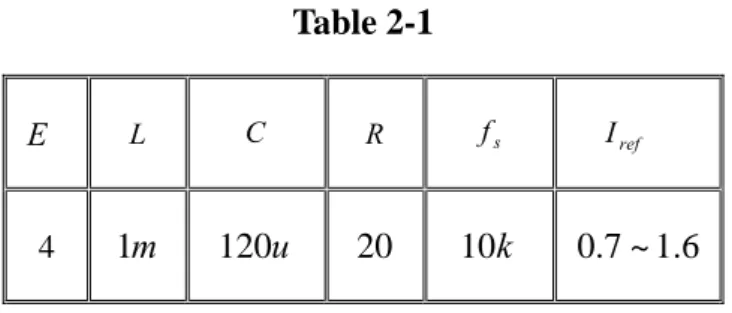
Table 2-1 L C R fs Iref E m 1 120u 20 10k 0.7~1.6 4
We define a set of specification in Table 1 and employ the Matlab tool to iterate (2.26). When
varies, the sampled data of the inductor always change, too. The bifurcation diagram
is presented in
ref
I iL
Fig.2-. We can find the way from a period-1 to chaos. When , the
system operates under period-1 state. When , the system is under the
period-doubling state. Finally, when the reference current increases up to a level,
, operating state can not be judged. We define the state to be a chaos state.
A Iref ≤0.87 A Iref >0.87 ref I A Iref >1.52
Chapter3
Design of Converters with Chaos Generator
Compared to the Chua’s circuit [22, 23], we propose a circuit as a chaotic generator. It is
similar to that discussed in[27] for the theory . It does not involve any inductor like other
popular chaos generator architectures such as Chua’s circuits; hence, it is particularly
compatible to fully analog on-chip realization
3.1 Modeling of Chaos Generator
Fig.3-1 Schematic of chaos generating circuit
DC voltage, two resisters, two switches, a comparator, a reference voltage, and a R-S latch.
The process is controlled by a set-rest latch. The clock signal is an impulse train at
frequency
T
fc=1. The impulse train is using a periodic waveform with a period T and a low duty cycle. Firstly, when clock generator sends a high level signal to R edge, Q edge is on high level and drives the switch1. The capacitor is charged by a voltage source
through a resister . In addition, the comparator provides a high level signal and sends to S
edge when the capacitor voltage reaches a reference voltage which is a desired value.
Therefore, sends a high level signal and makes the switch2 turn on. The capacitor is
discharged to ground through a resister . Because of the motion of the switches turning on
and off repeatedly, a signal of charging and discharging is produced.
C Vs 1 R R V Q C 2 R
Fig.3-2 shows the derivation of the capacitor voltage. When the switch1 is on, the
switch2 is off. Thus, the capacitor is charged. The behavior of the circuit is as
1 R v V dt dv C c = s − c (3.1)
,where Vc is the capacitor voltage.
When the switch2 is on, the switch1 is off. So, the capacitor is discharged. The behavior of the circuit is as 0 2 = + R v dt dv C c c (3.2) From (3.1), (3.2), we get R )) ( ( ) (t V V v n e 1 t t t v RC n t t c s s c n < < − − = − − (3.3)
1 ) ( 2 + − < < = RC R n t t R c t V e t t t v R −
Fig.3-2 The derivation of the capacitor voltage
In order to build a model of the circuit, we employ stroboscopic map to describe the
behavior of the circuit. First of all, as shown in Fig.3-2, we define a borderline voltage
and which is the value of at . When , the capacitor charges for a time
and is smaller than a period
(3.4) b V n V v(t) tn Vn >Vb t , n1 1 n
t T . On the other hand, whenVn<Vb, the capacitor charges and
the waveform has no effect on the next clock pulse until the . The time is over a
period
R
V tn1
T .
3.3), assuming that
From ( t =tR, tn1 =tR −tn, we can calculate thetn1as
R C R tn1 c s s V v n e V V −( − ( )) − 1 = ) V V (n) v V ( C R t R s c s n − − = ⇒ 1 1 ln (3.5)
From (3.5), if tn1 =T , the capacitor voltage is the borderline voltage V , b C R T R s s b c n V V V V e v ( ) ( ) 1 − − − = = (3.6) t
V
RV
boV
nV
n+1V
n+2 T n )1 ( +nT
(n 2)T 1 nt
2 nt
Rt
t
=
+Therefore, when vc(n)>Vb, the next sample value of the capacitor voltage is as C R T c s s c n V V v n e v ( 1) ( ( )) 1 − − − = + (3.7) Whenvc(n)<Vb, assuming 1 T t d = n and T t d n2
1− = we can get vc(n+1) from (3.4)
T C R d R C R t R c e V e V n v n 2 2 2 ) 1 ( ) 1 ( − − − = = + 2 1 2 ( ( )) R R R s c s C R T R V V n v V e V − − = − (3.8)
Therefore, from (3.7) and (3.8), the stroboscopic map of the system is as:
⎪ ⎪ ⎩ ⎪⎪ ⎨ ⎧ > − − ≤ − − = + − − ) ( ) ( )) ( ( ) 1 ( 2 1 2 1 b c R R R s c s C R T R b c C R T c s s c V n v ) V V (n) v V ( e V V n v e n v V V n v (3.9)
3-2 Simulation of Numerical Analysis
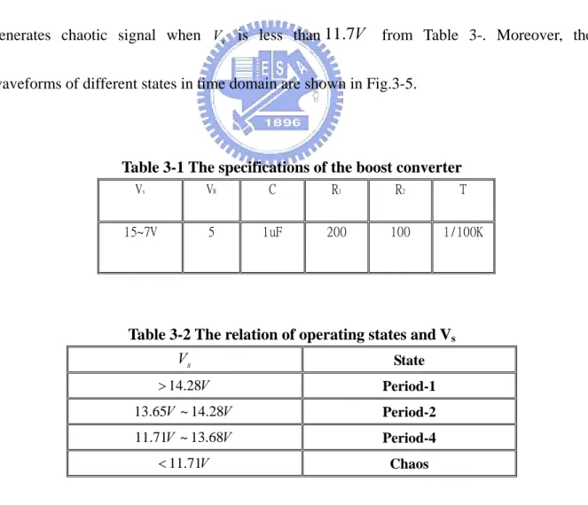
Fig.3-3 is the circuit frame of the new chaos generator. The circuit parameters are listed
in Table 3-1. Based on the iterating map from (3.9), we can generate the bifurcation diagram
handily and fast. By controlling the as the bifurcation parameter, we periodically collect
the discrete-time values of with the initial transient discarded. Thus, we have one set of
data for each value of
s
V
c
v
s
V . A bifurcation diagram can then be constructed after a sufficient
number of data sets are obtained as shown in Fig.3-4.
Fig.3-4 presents the results of the way from period-1 to chaos. The relationship of system
states and controlling parameter Vs is shown in Table 3-. It is worth noting that the circuit generates chaotic signal when Vs is less than11.7V from Table 3-. Moreover, the waveforms of different states in time domain are shown in Fig.3-5.
Table 3-1 The specifications of the boost converter
Vs VR C R1 R2 T
15~7V 5 1uF 200 100 1/100K
Table 3-2 The relation of operating states and Vs
s V State V 28 . 14 > Period-1 V V ~14.28 65 . 13 Period-2 V V ~13.68 71 . 11 Period-4 V 71 . 11 < Chaos
Fig.3- 4 Bifurcation Diagram of the Chaos Generator
(b) Period-2 (Vs=14V)
(d) Chaos (Vs=10V)
Fig.3-5 The waveforms of different states in time domain
3.3 A Current-Controlled Boost Converter without Chaos
Generators
Fig.3-6 blocks of the close loop circuit with constant frequency signal
operating condition of a boost converter without chaos generators. The system consists of a
DC-DC converter, a compensator, a current modulator, and a PWM modulator. Fig.3-6 shows
the blocks in close loop. When the system is at transient state, the output voltage and
reference voltage are always adjusted to the desired voltage level. The error signal produced
by the output voltage and reference voltage passes through the compensator which makes
system operate stably in period-1 state. A signal from the compensator becomes a peak level
of the inductor current to control the inductor current in current modulator block. Finally, in
the driving circuit block, a S-R flip-flop is controlled to generate a switch signal by the
constant frequency clock signal and the modulation signal. By adjusting the output voltage
continuously, a set of switching signals are produced to make the system stay in steady state.
When duty ratio is small than 0.5 in peak current control, it is stable in period-1 state.
Therefore we assume a specification of a boost converter operating in the period-1state:
5
.
0
~
2
.
0
,
40
,
100
,
140
,
32
~
20
max=
=
=
=
=
−Duty
V
V
kHz
f
W
P
V
V
o s o in (3.10)In addition, the simulations will be shown in Chapter 4.
Fig.3-7 blocks of the close loop circuit with chaotic signal Switch signal Chaotic signals Error signal Inductor current (a) Error signal Inductor current Chaotic signal Switch signal (b)
Fig.3-8 The behavior of driving circuit (a) the circuit of S-R flip-flop(b) the signals of
Compared with Fig.3-6, the main point in Fig.3-7 is the block of driving circuit. A set of
chaotic clock signals and modulation signals are used for a S-R flip-flop. In Fig.3-8(a),
because the signal of S-R flip-flop can control the switch to turn on: therefore a system
can be operated to be under the chaos state when the signal of S-R flip-flop is chaotic. It
is worth noting that the switch is still to be on when the inductor current charges and
Q
S
R
signal have a pulse at that time. Fig.3-8(b) illustrates the behavior of driving circuit.
3.5 Analysis of Stability of a Boost Converter with Chaos
Generators
Because important point is stability for a DC-DC converter, therefore we analyze the
stability of a boost converter with chaos generator in the section
3.5.1 The Clopes of Charge and Discharge of an Inductor Current in a
Boost Converter under Current Mode Control
Fig.3-9 presents the behavior of the inductor current waveform of the boost converter
under current mode control. When the inductor charges, the slope of the inductor is yielded:
1 , m L E T d i I n n L ref − = = (3.11)
Where Iref is a reference current, Eis the input voltage. When the inductor discharges, the slope of the inductor is yielded:
2 1 , ) 1 ( L m v E T d i I c n n L ref =− − = − − + (3.12)
When the system is in the steady sate, the is constant. Therefore, from (18) and (19),
is constant in the steady state.
c
v and
1
m m2
3.5.2 The Influence of the Gain of PWM Circuit and Current Modulator
Fig.3-10 Block diagrams of a close-loop for a power converter with current control
In the beginning, we must analyze the influence of the gain of driving circuit and current
modulator when the clock signal is varying. Fig.3-10 presents block diagrams of a close loop
modulator and current modulator. Fig.3-11 analyzes in detail the influence. There are an
inductor current in the steady state, the rising slope of an inductor current, duty ratios,
different currents ,the reference currents , , and varying frequency clock signals in
Fig.3-11. The relations of duty ratio and the difference of reference current are presented in
the following expression:
1 ref I Iref2 1 2 1 1 1 2 1 ) 1 1 ( m I I T T D D I d ref ref ref = − − = Δ Δ (3.13) 1 2 1 3 3 3 3 ' ) 1 1 ' ( m I I T T D D I d ref ref ref = − − = Δ Δ (3.14)
When the system is in the steady state, the slopes of charge and discharge of an inductor
current are constant. Therefore, (3.13) and (3.14) depict that the gain are not affected in
despite of the varying frequency of clock signals.
Fig.3-11 The inductor current waveform for different reference currents
Fig.3-12 The inductor current waveform in period-1
Fig.3-12 indicates the behavior of an inductor current in steady state under period-1 state.
We assume the duty ratio D and period T are as:
4 3 2 1 D D D D D= = = = (3.15) 4 3 2 1 T T T T T = = = = (3.16) D T T T D T D T T D Dave period = + + = = − 2 1 2 2 1 1 1 1 1 1 _ (3.17)
In addition, because of the slopes of charge and discharge for an inductor current, we can
define the peak-to-peak value of the inductor current isΔI. Thus the slope of charge and the slope of discharge are as:
1 m 2 m 1 1 1 T D I m = Δ (3.18) 1 1 2 ) 1 ( D T I m − Δ − = (3.19)
1 2 2 1 m m m D D − = = (3.20)
3.5.4 Analysis of Period-2
L
i
DT T T D) 1 ( − I Δ 2 m ref IClock
1 mFig.3-13 The inductor current waveform in a period T
Fig.3-14 The inductor current waveform in period-2
peak-to peak value of the inductor current and a periodT . From Fig.3-13, (3.18) and (3.19),
and can be as:
1 2 m m 1 2 2 1 m m T m m I − = Δ (3.21)
So, from (3.20), we can know
T
I∝
Δ (3.22)
Because the clock frequency becomes slower, the duration that an inductor current
charge and the period of an inductor current is in the period-2 state. Fig.3-14, we assume the
relation of duty ratioD', a period T , and duty ratio in the period-2 state are as: '
(3.23) ' 4 ' 3 ' 2 ' 1 ' D D D D D = = = = (3.24) ' ' ' ' 4 3 2 1 ' 2T =T =T =T =T =T ' ' ' 1 ' 1 1 T D I T D I m = Δ ' = Δ ' (3.25) From (3.23), becauseT' =2T , I I = Δ Δ ' 2 (3.26) From(3.11), (3.18), (3.19), (3.25) and (3.26) L E m1 = = constant = ' ' ' T D I DT ΔI = Δ (3.27) DT T D' ' =2 => (3.28)
So, the average duty ratio in period-2 state is as: D T DT T T T T T D T D T D T D Dave period = = + + + + + + = − 8 8 ' 4 ' 3 ' 2 ' 1 ' 4 ' 4 ' 3 ' 3 ' 2 ' 2 ' 1 ' 1 2 _ (3.29)
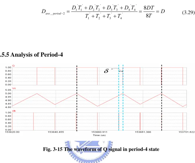
3.5.5 Analysis of Period-4
Fig. 3-15 The waveform of Q signal in period-4 state
Because clock signal is mainly generated by Q signal ,we observe the Q signal by chaos
signal. From Fig.3-15, because the quality of chaos, a small difference causes period-2 state to
be period-4 state. ref I Clock L
i
'' 1 '' 1T D '' 2 '' 2T D 3'' '' 3T D '' 4 '' 4T D '' 1 T '' 2 T '' 3 T '' 4 T δ 1 m m2 m1 2 ' m 1 I Δ 2 I ΔFig.3-16 presents the inductor current waveform in period-4 state. We define a period in
the period-4 state as '', where , and
2 '' 1 T T + '' = '+δ 1 T T '' = '−δ 1 T
T δ have small differences.
The dotted line presents the inductor current in the period-2 state and the solid line presents
the inductor current in the period-4 state. Because a pulse of clock signal delays in period-4
state, the duration of the inductor discharged becomes longer. Besides, because the slope of
discharge of the inductor current is equal to
L E t v
m =− out( )−
2 , it results in the inconsistency
the slope of discharge of the inductor current. But the slope of charge of the inductor current
is still constant. From Fig.3-16, we define the slopes as:
'' 1 '' 1 1 1 T D I m = Δ = '' 2 '' 2 2 T D I Δ (3.30) '' 1 '' 1 2 2 ) 1 ( D T I m − Δ − = (3.31) '' 2 '' 2 1 ' 2 ) 1 ( D T I m − Δ − = (3.32) , where m2 ≠m2'
We assume the peak-to-peak values of the inductor current are ΔI1, IΔ 2 as shown in Fig.3-16.
The relations of Δ and the slope of inductor current are as: I
δ 1 2 2 1 ' 1 2 2 1 1 m m m m T m m m m I + − + − = Δ (3.33) δ 1 2 2 1 ' 1 2 2 1 2 m m m m T m m m m I + + − = Δ (3.34)
From (3.22) and Fig.3-16, we can know 1 '' '' , m I T D T I∝ = Δ Δ (3.35)
Therefore the expressions can present as:
δ 1 2 2 ' 1 2 2 '' 1 '' 1 m m m T m m m T D + − + − = (3.36) 1 2 2 ' 1 2 2 '' 2 '' 2 δ m m m T m m m T D + + − = (3.37)
From (3.20), (3.36), and (3.37) the average duty ratio is as:
D m m m T T D T D T T T D T D Dave period = − = + = + + = − 1 2 2 ' '' 2 '' 2 '' 1 '' 1 '' 2 '' 1 '' 2 '' 2 '' 1 '' 1 4 _ 2 (3.38)
3.5.6 Analysis of Chaos
ref I Li
Clock
Ton1 Ton2 Ton3 Ton4 Ton5 Ton6
Duty ratio
Fig.3-17 The inductor current (clock frequency is increasing)
It is complex to analyze the duty ratio in the chaos state. However, we can divide two
constant, the duration that the switch is on is constant in steady state. However, when the
frequency of clock signal is increasing, that isTon2<Ton1, it results that duration that the switch
is on is longer the duration that the switch is off. Fig.3-17 shows that the behavior of the
circuit is controlled byT . In conclusion, the output voltage will be lower when the inductor
current is increasing.
on
On the other hand, the duration that the switch is off is longer when the frequency of
clock signal is decreasing. Fig.3-18 presents that the behavior of the circuit is controlled by
and the behavior of the circuit is controlled byT .
off
T off
Toff1 Toff2 Toff3
ref I
Clock
Toff4 Toff5 Li
Duty ratioFig.3-18 The inductor current (clock frequency is decreasing)
From analysis of the above, some conclusions can be known.
1. The gain of the current modulator circuit is constant:
Because the operating frequency of system is changed by chaos clock signals in feedback
control, the performance of system seems be affected. Practically, the slopes of charge and
gain of the current modulator circuit by changing the clock frequency.
2. The average output voltage is not affected:
In steady observation, the stability of a converter is decided by duty ratio. From the
analysis of quasi-period, we know the average output voltage is the same in despite of
period-1, period-2, period-4 or chaos states. In transient observation, because the frequency of
clock signal under chaos state is broadband and well mixed, therefore frequency of clock
frequency is longer or shorter at different time and it affects the duration of charge or
discharge of an inductor and then the output voltage ripple is affected. In chaos analysis of the
above, the average value of the voltage ripple is zero. So the average output voltage is not
Chapter 4
Simulation Result and Analysis
To prove accuracy for the analysis of the Chpater3, we employ the PSIM and Matlab
numerical tools to accomplish the circuit simulation.
4.1The Circuit Frame of a Current-Controlled Boost Converter
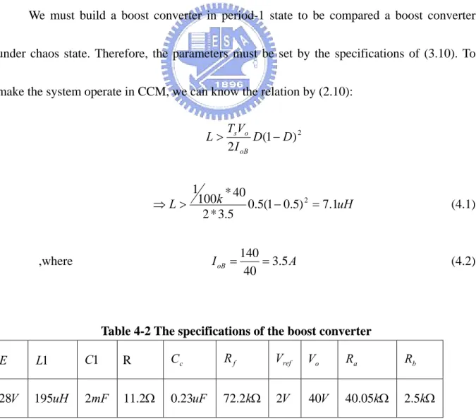
We must build a boost converter in period-1 state to be compared a boost converterunder chaos state. Therefore, the parameters must be set by the specifications of (3.10). To
make the system operate in CCM, we can know the relation by (2.10):
2 ) 1 ( 2I D D V T L oB o s − > uH k L 0.5(1 0.5) 7.1 5 . 3 * 2 40 * 100 1 2 = − > ⇒ (4.1) ,where IoB 3.5A 40 140 = = (4.2)
Table 4-2 The specifications of the boost converter
E L1 C1 R Cc Rf Vref Vo Ra Rb
V
The circuit frame of boost converter by PSIM is shown in Fig.4-1. We set a specification
that input E =28V raises to output Vo =40V . Other parameters are shown in Table 4-1.
Fig.4-1 Circuit diagram of the current-controlled boost converter
Because we must promise that the boost converter works under the stable period-1 state,
we add a compensator in the feedback loop to the system be stable. Fig.4-2 presents the
circuit of the compensator. The circuit consists of an Op amplifier, resisters, and a capacitor.
One point is worth making about Fig.4-2. A circuit of divided voltage is built to protect Op
amplifier from high voltage. Therefore, is not equal to and the relation of and
is yielded: ref V Vo Vref o V o b a b ref V R R R V + = (3.12)
Because our goal mainly focus on chaos behavior, the compensator of the boost
converter considered is described in [28].
Fig.4-2 The compensator
The simulation of the close loop circuit is generated by PSIM simulation tool. The result
is shown in Fig.4-3. Fig.4-3 presents that the system keeps in stable period-1 state and the
inductor current is in continuous condition mode.
(a) Simulation of the output voltage
(b) Simulation of the inductor current Fig.4-3 Simulation of the boost converter by PSIM
Secondly, we employ the PSIM and Matlab numerical tools to accomplish the circuit
including a boost converter, a compensator, a driving circuit, and a chaos generator. The
specification presents in Table 3-1 and Table 4-1.
Fig.4-4 The circuit frame of a boost converter with chaos generator
4.2 Simulation of Stability
When the input voltage of chaos generator,V , is adjusted to be quasi-period state, the
simulations present in following simulation diagrams. From Fig.4-5 to Fig.4-8, every average
duty ratio and average output voltage are as:
s
3 0 10 10 3 5 6 1 _ . * D -period ave − = = and ~ =vo 40V
2. When Vs =12.5V, the system is in period-2 state 3 0 10 2 10 6 5 6 2 _ . * * D -period ave − = = and ~ =vo 40V
3. When Vs =11.8V, the system is in period-4 state 3 0 10 4 10 7 10 5 5 6 6 4 _ . * * * D -period ave = + = − and ~ =vo 40V
4. When Vs =10V, the system is under chaos state
3 . 0 .. 304 . 0 10 * 9 . 2 10 * 7 ... 10 * 9 10 * 5 10 * 3 10 10 * 9 10 * 5 10 10 * 4 4 6 6 6 6 6 6 6 5 6 _ ≈ = + + + + + + + + = − − − − − − − − − − chaos ave D and ~ =vo 40V
Fig.4-6 Simulation in Period-2(Vs=12.5V)
Fig.4-8 Simulation in Chaos(Vs=10V)
In addition, from Fig.4-9, because the frequency is broadband and the time of charge and
discharge for the inductor current, therefore the output voltage ripple vibrates slightly.
However, the average output voltage is be 40V stably.
4.3 Response of Output Voltage to loading current
Fig.4-10 The circuit for testing varying loading
Fig.4-11 The testing circuit of testing varying loading
When loading is varying, the stability may change. We add and pump the loading circuit
to test the stability of the boost converter with chaos generator. The simulation circuit is
shown in Fig.4-10. The testing circuit is shown in Fig.4-11. We add a loading current of
original 20% loading current and then pump it from the converter. From Table 4-1, the
original current is yielded:
A R V I o o 3.57 2 . 11 40 1 = = =
The simulation result is shown in Fig.4-12. We can observe that the output voltage still retain
to be 40V in the steady state even through loading is varying.
Fig.4-12 Simulation of load current change
4.4 Clock Times of Frequency for the clock signal
Fig.4-13 The statistical chart of the clock times of frequency for the clock signal
different frequencies of chaotic signal by chaos generator for some duration is shown in
Fig.4-13. The total times of frequencies are 13400 times. We can observe that the clock times
of frequencies for the clock signal are dispersed. In addition, because the characteristic of
chaos, the clock times of low frequencies are more and cause the power in low frequency is
higher.
4.5 Simulation of PSD
Secondly, we get data of simulation in PSM and calculate PSD by Matlab tool. The
following are the simulation diagrams of PSD in quasi-period. The power in quasi-period
states calculated by Matlab is shown in Table 4-5. Therefore, in spite of the different operating
states, every power is still the same. Compare the period-1 state with different operating state
form Fig.4-14 to Fig.4-18, the results present the degree of reduction and are shown in Table
4-2, Table 4-3, and Table 4-4. Table 4-5 shows the power in different states is the same. In
Fig.4-14, we can observe that there is obviously discrete spectrum in period-1 state and peak
values of harmonics in period-2 state have reduced. Fig.4-15 and Fig.4-16 show the spectrum
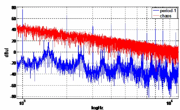
in period-4 state. There is the continue spectrum under chaos in Fig.4-17. Fig.4-18 shows the
obvious difference with period-1 and chaos state. Because power is constant and chaos is
broadband, the peak values in harmonics originally are reduced. Therefore, the chaos can
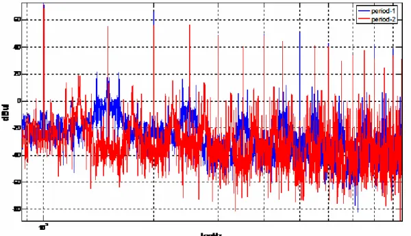
Fig.4-14 Simulation of PSD (Period-1 and Period-2)
Table 4-2 Degree of reduction(Period-1 & Period-2) fs Perios-1 (dBul) Period-2 (dBul) Reduction (dBul) 1 76.33384 71.71917 4.614664 2 65.69836 55.49231 10.20604 3 48.59668 48.45855 0.438125 4 49.47079 47.62989 1.840904 5 50.21335 44.3838 5.82955 6 42.43602 40.58597 1.850049 7 34.14725 33.70555 0.441701 8 41.60542 35.41556 6.18986 9 38.15995 33.52151 4.638447
Fig.4-15 Simulation of PSD (Period-1 and Period-4)
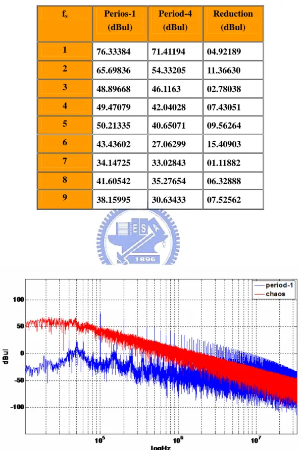
Table 4-3 Degree of reduction(Period-1 & Period-4) fs Perios-1 (dBul) Period-4 (dBul) Reduction (dBul) 1 76.33384 71.41194 04.92189 2 65.69836 54.33205 11.36630 3 48.89668 46.1163 02.78038 4 49.47079 42.04028 07.43051 5 50.21335 40.65071 09.56264 6 43.43602 27.06299 15.40903 7 34.14725 33.02843 01.11882 8 41.60542 35.27654 06.32888 9 38.15995 30.63433 07.52562
Fig.4-18 Amplification of simulation of PSD (Period-1 and chaos)
Table 4-4 Degree of reduction(Period-1 & Chaos) fs Perios-1 (dBul) Chaos (dBul) Reduction (dBul) 1 76.33384 42.2693018 33.06453 2 65.69836 35.7387797 29.95958 3 48.89668 30.656851 18.23982 4 49.47079 25.5436384 23.92715 5 50.21335 26.1424526 24.07089 6 43.43602 20.6228786 21.81314 7 34.14725 14.5116641 19.63558 8 41.60542 16.6259601 24.97945 9 38.15995 13.8021154 24.35783
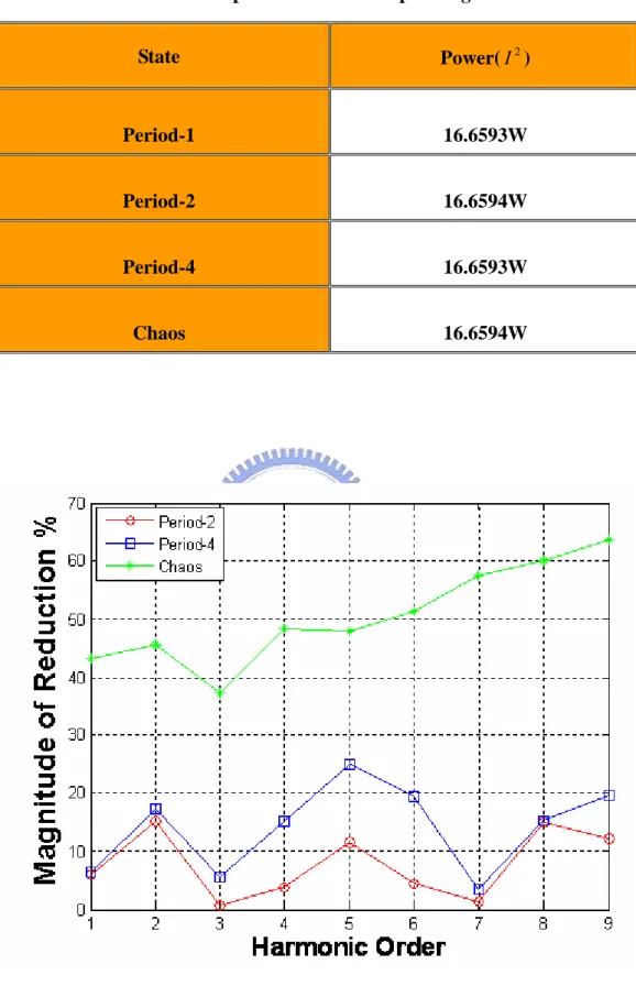
Table 4-5 The power in different operating states State Power(I ) 2 Period-1 16.6593W Period-2 16.6594W Period-4 16.6593W Chaos 16.6594W
Fig.4-19 The relation of Reduction percent and harmonics