Enhanced reliability of electroluminescence from metal–oxide–silicon
tunneling diodes by deuterium incorporation
C. W. Liu,a)C.-H. Lin, M. H. Lee, S. T. Chang, Y.-H. Liu, Miin-Jang Chen,b) and Ching-Fuh Linb)
Department of Electrical Engineering, National Taiwan University, Taipei, Taiwan, Republic of China 共Received 7 November 2000; accepted for publication 8 January 2001兲
The reliability of electroluminescence from metal–oxide–silicon 共MOS兲 tunneling diodes was improved by the incorporation of deuterium. The deuterium was incorporated by the deuterium prebake and the postoxide deuterium annealing. At constant current stress of 100 mA, a deuterium-treated n-channel MOS tunneling light-emitting diode shows that the integrated light emission intensity increases slightly about 6% after 10 000 s operation, while the hydrogen-treated device shows a 30% decrease of the integrated light emission intensity. The hydrogen release by the electrons tunneling from the gate electrode to Si and the formation of interface defects are responsible for the degradation of light output in the hydrogen-treated samples. An annealing model is also given to explain the slight increase of light output in the deuterium-treated samples. © 2001
American Institute of Physics. 关DOI: 10.1063/1.1353817兴
The electrical degradation of metal–oxide–silicon 共MOS兲 devices due to current stress has been extensively studied since the early 1980s.1The degradation is attributed to the hydrogen release from the Si/oxide interface by hot electrons2and the incorporation of deuterium at the Si/oxide interface can significantly improve the device reliability.3 The strong coupling between Si–D bending mode 共460 cm⫺1) and transverse optical phonons in bulk Si共463 cm⫺1) is responsible for this giant isotope effect.4,5 Recently, the band-edge electroluminescence from metal–oxide–silicon tunneling diodes has been observed.6 The emission line shapes can be fitted by an electron-hole-plasma model and the enhanced light emission is attributed to the Si/oxide in-terface roughness7 and phonons.8 However, the light emis-sion intensity degrades after the current stress.9In this letter, we perform deuterium prebake and postoxide deuterium an-nealing to incorporate deuterium at the Si/oxide interface, and demonstrate that the deuterium-treated device has stron-ger reliability than the hydrogen-treated device.
The ultrathin gate oxide of the MOS tunneling diode used in this study is grown by rapid thermal oxidation共RTO兲 on p-type Si at the 900 °C. The gas flows are 500 sccm nitrogen and 500 sccm oxygen at the pressure of 100–250 mbar. Before oxidation, the sample was cleaned by a HF dip. An in situ deuterium prebake at 900 °C for 2 min was per-formed before the growth of the RTO. After the growth of ultra thin oxide 共1–3 nm兲, the sample was postannealed in deuterium at 900 °C for 10 min and in nitrogen at 900 °C for another 10 min. This yields a deuterium concentration of 2 ⫻1020 cm⫺3 in a 2.5 nm oxide measured by the secondary ion mass spectroscopy 共SIMS兲 共Fig. 1兲. To avoid the other signal with mass-to-charge ratio of 2 such as H2⫹, the SIMS profiles of a hydrogen-treated sample was also measured, and this signal is 1⫻1018cm⫺3, which is negligible as
com-pared to the deuterium concentration. This deuterium con-centration is higher than the reported value of 5⫻1019cm⫺3 by postgate-electrode annealing.4 The SIMS measurement also indicates that the deuterium prebake without postoxide annealing produces a much lower deuterium concentration (⬃1019cm⫺3) in oxide. The hydrogen-treated samples were processed in the exactly same procedure except replacing deuterium by hydrogen. The wafer temperature was mea-sured by a pyrometer with a close loop control. The thick-ness is measured by ellipsometry. The resistivity of the 100 mm p-type 共100兲 wafers is 1–10 ⍀ cm. The N 共n-channel兲 MOS diodes have Al gate electrodes with circular areas de-fined by photolithography.
The light emission is obtained by biasing the NMOS tunneling diode at accumulation region, i.e., applying the negative voltage on the gate electrode. Due to the ultrathin oxide, the electron tunnels into the p-type Si through the ultrathin oxide, and recombines with the hole in the accumu-lation region, which is formed by the negative gate voltage. The band edge light emission can be observed if the surface/ interface roughness and phonons can provide the necessary
a兲Also at: Graduate Institute of Electronic Engineering; electronic mail: [email protected]
b兲Also at: Institute of Electro-Optical Engineering. FIG. 1. SIMS profiles of deuterium, silicon, and oxygen in the rapid thermaloxide with deuterium prebake and the postoxide deuterium annealing.
APPLIED PHYSICS LETTERS VOLUME 78, NUMBER 10 5 MARCH 2001
1397
0003-6951/2001/78(10)/1397/3/$18.00 © 2001 American Institute of Physics
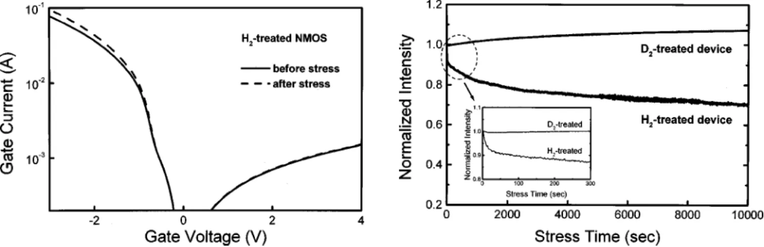
momentum. Figure 2 shows the initial emission spectrum of a hydrogen-treated NMOS diode with oxide thickness of ⬃1 nm and an area size of 5⫻10⫺3 cm2 under 100 mA current operation. After 10 000 s constant current stress共100 mA,⬃⫺3 V兲, the final emissions spectrum is also shown in Fig. 2. It is obvious that the integrated intensity decreases ⬃30% after the stress. The theoretical line shapes based on the electron-hole-plasma model are also shown in Fig. 2.6 Under the constant current stress, the hydrogen bounded with Si at Si/oxide interface was released due to the energy trans-fer from the tunneling electrons, and therefore, the interface state density increases. The interface states act as the nonra-diative recombination centers between the holes in the accu-mulation region and the electrons tunneling from gate elec-trode to p-Si. Therefore, the light emission 共radiative recombination兲 of hydrogen-treated device decreases after the constant current stress. Due to the release of hydrogen, trap creation occurs in the oxide.10 The I–V curve shows a significant stress-induced-leakage current in the accumula-tion bias, as shown in Fig. 3.
For deuterium prebaked and postoxidation-annealed samples, the NMOS diodes with thickness of⬃1 nm and an area size of 5⫻10⫺3cm2was fabricated in the same process as the hydrogen-treated samples The electroluminescence spectra of the deuterium-treated NMOS diode before and af-ter a constant stress 共100 mA and 10 000 s兲 with voltage of
⬃⫺3 V are very similar, and the difference in the integral intensity is about 6%. However, the interesting feature is that after stress, the emission intensity becomes stronger than the initial intensity. The origin of this feature is not exactly known, but this observation is very carefully checked, and is repeatable for all measured deuterium-treated devices. A cur-rent annealing effect may be responsible for this. The opera-tion current of 100 mA with gate voltage of⬃⫺3 V gener-ated 60 W/cm2joule heat on the diode, and the local heating of the device probably occurs. The local heating might drive the unbounded deuterium to bind with the Si, and thus the interface state density decreases. Due to the strong coupling between Si–D and phonons, the electron tunneling from gate electrode to Si can hardly break the Si–D bond.11 The I–V curves of the deuterium-treated device before and after the stress change much less共the inset of Fig. 4兲, as compared to the hydrogen-treated device 共Fig. 3兲. The higher deuterium concentration (2⫻1020cm⫺3) in our sample, as compared to Ref. 4, indicates the possibility of the existence of unbound deuterium. The temperature for postgate-electrode deuterium annealing is low共400–450 °C兲, and both deuterium diffusion and bonding with Si occur at such low temperature. It is believed that the Si–D bond formation can occur at a tem-perature below 400 °C, which can be possibly done by local
FIG. 5. Time evolution of the emission intensity at peak for both deuterium-treated and hydrogen-deuterium-treated devices.
FIG. 2. The electroluminescence spectra of a hydrogen-treated NMOS diode before and after stress. The stress condition is 100 mA for 10 000 s.
FIG. 3. The current–voltage curves of a hydrogen-treated NMOS diode before and after stress. The stress condition is 100 mA for 10 000 s.
FIG. 4. The electroluminescence of a deuterium-treated NMOS diode before and after stress. The stress condition is 100 mA for 10 000 s. The inset is the
I–V curves before and after stress.
1398 Appl. Phys. Lett., Vol. 78, No. 10, 5 March 2001 Liuet al.
joule heating. The decrease of interface state density makes the nonradiative recombination rate via the interface states to decrease, and thus the radiative recombination rate increases at the constant current operation.
To measure the time evolution of the emission intensity, the emission intensity at the peak of the spectra was moni-tored. The normalized emission intensity at peak of the spec-tra 共not integrated intensity兲 for deuterium-treated samples increases initially with the operation time 共Fig. 5兲, and satu-rated at a 7% increase after 10 000 s stress at 100 mA, cor-responding to a fluence of 2⫻105 C/cm2. For the hydrogen-treated sample, the tunneling electron continues to release the hydrogen from the Si–H bond and thus increases the interface state density. The nonradiative recombination rate via interface states increases with the operation time. There-fore, the light emissions intensity at the peak of the spectra decreases and drops approximately 30% after 10 000 s stress at 100 mA共a fluence of 2⫻105 C/cm2). both devices show more significant changes at the early stage of the stress pe-riod. Especially for the hydrogen-treated device, the intensity drops 10% within initial 50 s共the inset of Fig. 5兲.
In summary, the reliability of band edge light emissions from the NMOS light emitting diode is improved by the deuterium prebake and postoxide deuterium annealing. The deuterium incorporation was demonstrated with a
concentra-tion of deuterium as high as 2⫻1020cm⫺3at Si/oxide inter-face and bulk oxide. Due to the strong coupling between Si–D bond and phonons, the emission intensity of D2-treated NMOS light-emitting diode shows much improved reliability as compared with H2-treated device.
This work is supported by TSMC and National Science Council 共Grant Nos. 002-082 and 89-2218-E-002-054兲, Taiwan, ROC.
1J. Maserijian and N. Zamini, J. Appl. Phys. 53, 559共1982兲. 2D. J. DiMaria and E. Cartier, J. Appl. Phys. 78, 3883共1995兲. 3
J. W. Lyding, K. Hess, and I. C. Kizilyalli, Appl. Phys. Lett. 68, 2526 共1996兲.
4K. Hess, I. C. Kizilyalli, and J. W. Lyding, IEEE Trans. Electron Devices 45, 406共1998兲.
5C. G. Van de Walle and W. B. Jackson, Appl. Phys. Lett. 69, 2441共1996兲. 6
C. W. Liu, M. H. Lee, M.-J. Chen, I. C. Lin, and C.-F. Lin, Appl. Phys. Lett. 76, 1516共2000兲.
7C. W. Liu, M. H. Lee, M. J. Chen, C.-F. Lin, and M. Y. Chern, IEEE Electron Device Lett. 21, 601共2000兲.
8
C. W. Liu, M.-J. Chen, I. C. Lin, M. H. Lee, and C.-F. Lin, Appl. Phys. Lett. 77, 1111共2000兲.
9C. W. Liu, M. H. Lee, S. T. Chang, M.-J. Chen, and C.-F. Lin, Jpn. J. Appl. Phys., Part 2 39, L1016共2000兲.
10D. J. DiMaria, E. Cartier, and D. A. Buchanan, J. Appl. Phys. 80, 304 共1996兲.
11J. H. Wei, M. S. Sun, and S. C. Lee, Appl. Phys. Lett. 71, 1498共1997兲. 1399
Appl. Phys. Lett., Vol. 78, No. 10, 5 March 2001 Liuet al.